


No CrossRef data available.
Article contents
Quantification of Ion-Implanted Single-Atom Dopants in Monolayer MoS2 via HAADF STEM Using the TEMUL Toolkit
Published online by Cambridge University Press: 20 June 2022
Abstract
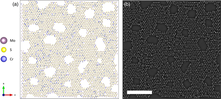
In recent years, atomic resolution imaging of two-dimensional (2D) materials using scanning transmission electron microscopy (STEM) has become routine. Individual dopant atoms in 2D materials can be located and identified using their contrast in annular dark-field (ADF) STEM. However, in order to understand the effect of these dopant atoms on the host material, there is now the need to locate and quantify them on a larger scale. In this work, we analyze STEM images of MoS2 monolayers that have been ion-implanted with chromium at ultra-low energies. We use functions from the open-source TEMUL Toolkit to create and refine an atomic model of an experimental image based on the positions and intensities of the atomic columns in the image. We then use the refined model to determine the likely composition of each atomic site. Surface contamination stemming from the sample preparation of 2D materials can prevent accurate quantitative identification of individual atoms. We disregard atomic sites from regions of the image with hydrocarbon surface contamination to demonstrate that images acquired using contaminated samples can give significant atom statistics from their clean regions, and can be used to calculate the retention rate of the implanted ions within the host lattice. We find that some of the implanted chromium ions have been successfully integrated into the MoS2 lattice, with 4.1% of molybdenum atoms in the transition metal sublattice replaced with chromium.
- Type
- Materials Science Applications
- Information
- Copyright
- Copyright © The Author(s), 2022. Published by Cambridge University Press on behalf of the Microscopy Society of America
Footnotes
†
Present address: Max Planck Institute for the Science of Light and Max-Planck-Zentrum für Physik und Medizin, Erlangen, Germany.
References
Bangert, U, Pierce, W, Kepaptsoglou, DM, Ramasse, Q, Zan, R, Gass, MH, Van den Berg, JA, Boothroyd, CB, Amani, J & Hofsäss, H (2013). Ion implantation of graphene — Toward IC compatible technologies. Nano Lett 13(10), 4902–4907. doi:10.1021/nl402812yCrossRefGoogle ScholarPubMed
Bangert, U, Stewart, A, O'Connell, EN, Courtney, E, Ramasse, Q, Kepaptsoglou, D, Hofsäss, H, Amani, J, Tu, J-S & Kardynal, B (2017). Ion-beam modification of 2-D materials — Single implant atom analysis via annular dark-field electron microscopy. Ultramicroscopy 176, 31–36. doi:10.1016/j.ultramic.2016.12.011CrossRefGoogle ScholarPubMed
Barthel, J (2018). Dr. Probe: A software for high-resolution STEM image simulation. Ultramicroscopy 193, 1–11. doi:10.1016/j.ultramic.2018.06.003CrossRefGoogle ScholarPubMed
Batson, PE, Dellby, N & Krivanek, OL (2002). Sub-ångstrom resolution using aberration corrected electron optics. Nature 418(6898), 617–620. doi:10.1038/nature00972CrossRefGoogle ScholarPubMed
Dean, CR, Young, AF, Meric, I, Lee, C, Wang, L, Sorgenfrei, S, Watanabe, K, Taniguchi, T, Kim, P, Shepard, KL & Hone, J (2010). Boron nitride substrates for high-quality graphene electronics. Nat Nanotechnol 5(10), 722–726. doi:10.1038/nnano.2010.172CrossRefGoogle ScholarPubMed
De Backer, A, van den Bos, KHW, Van den Broek, W, Sijbers, J & Van Aert, S (2016). StatSTEM: An efficient approach for accurate and precise model-based quantification of atomic resolution electron microscopy images. Ultramicroscopy 171(2016), 104–116. doi:10.1016/j.ultramic.2016.08.018CrossRefGoogle ScholarPubMed
De La Peña, F, Prestat, E, Tonaas Fauske, V, Burdet, P, Lähnemann, J, Jokubauskas, P, Furnival, T, Nord, M, Ostasevicius, T, MacArthur, KE, Johnstone, DN, Sarahan, M, Aarholt, T, Taillon, J, Migunov, V, Eljarrat, A, Caron, J, Francis, C, Nemoto, T, Poon, T, Mazzucco, S, Tappy, N, Cautaerts, N, Somnath, S, Slater, T, Walls, M & Winkler, F (2021). hyperspy/hyperspy: Release v1.6.4. Zndo. doi:10.5281/ZENODO.592838CrossRefGoogle Scholar
De wael, A, De Backer, A, Jones, L, Nellist, PD & Van Aert, S (2017). Hybrid statistics-simulations based method for atom-counting from ADF STEM images. Ultramicroscopy 177, 69–77. doi:10.1016/j.ultramic.2017.01.010CrossRefGoogle ScholarPubMed
Dolui, K, Rungger, I, Pemmaraju, CD & Sanvito, S (2013). Ab-initio study on the possible doping strategies for MoS2 monolayers, pp. 1–9. doi:10.1103/PhysRevB.88.075420CrossRefGoogle Scholar
Dumcenco, DO, Kobayashi, H, Liu, Z, Huang, YS & Suenaga, K (2013). Visualization and quantification of transition metal atomic mixing in Mo1-xWxS2 single layers. Nat Commun 4. doi:10.1038/ncomms2351CrossRefGoogle ScholarPubMed
Giovannetti, G, Khomyakov, PA, Brocks, G, Karpan, VM, Van Den Brink, J & Kelly, PJ (2008). Doping graphene with metal contacts. Phys Rev Lett 101(2), 4–7. doi:10.1103/PhysRevLett.101.026803CrossRefGoogle ScholarPubMed
Gong, Y, Liu, Z, Lupini, AR, Shi, G, Lin, J, Najmaei, S, Lin, Z, Elías, AL, Berkdemir, A, You, G, Terrones, H, Terrones, M, Vajtai, R, Pantelides, ST, Pennycook, S, Lou, J, Zhou, W & Ajayan, P(2014). Band gap engineering and layer-by-layer mapping of selenium-doped molybdenum disulfide. Nano Lett 14(2), 442–449. doi:10.1021/nl4032296CrossRefGoogle ScholarPubMed
Hansen, LP, Ramasse, QM, Kisielowski, C, Brorson, M, Johnson, E, Topsøe, H & Helveg, S (2011). Atomic-scale edge structures on industrial-style MoS2 nanocatalysts. Angew Chem Int Ed 50(43), 10153–10156. doi:10.1002/anie.201103745CrossRefGoogle ScholarPubMed
Hjorth Larsen, A, Jørgen Mortensen, J, Blomqvist, J, Castelli, IE, Christensen, R, Dułak, M, Friis, J, Groves, MN, Hammer, B, Hargus, C, Hermes, ED, Jennings, PC, Jensen, PB, Kermode, J, Kitchin, JR, Kolsbjerg, EL, Kubal, J, Kaasbjerg, K, Lysgaard, S, Maronsson, JB, Maxson, T, Olsen, T, Pastewka, L, Peterson, A, Rostgaard, C, Schiøtz, J, Schütt, O, Strange, M, Thygesen, KS, Vegge, T, Vilhelmsen, L, Walter, M, Zeng, Z & Jacobsen, KW (2017). The atomic simulation environment – A python library for working with atoms. J Phys Condens Matter 29, 27. doi:10.1088/1361-648X/aa680eCrossRefGoogle ScholarPubMed
Hosokawa, F, Sawada, H, Kondo, Y, Takayanagi, K & Suenaga, K (2013). Development of Cs and Cc correctors for transmission electron microscopy. J Electron Microsc 62(1), 23–41. doi:10.1093/jmicro/dfs134Google ScholarPubMed
Jiang, Y, Chen, Z, Han, Y, Deb, P, Gao, H, Xie, S, Purohit, P, Tate, MW, Park, J, Gruner, SM, Elser, V & Muller, DA (2018). Electron ptychography of 2D materials to deep sub-ångström resolution. Nature. doi:10.1038/s41586-018-0298-5CrossRefGoogle Scholar
Karthikeyan, J, Komsa, HP, Batzill, M & Krasheninnikov, AV (2019). Which transition metal atoms can be embedded into two-dimensional molybdenum dichalcogenides and add magnetism? Nano Lett 19(7), 4581–4587. doi:10.1021/acs.nanolett.9b01555CrossRefGoogle ScholarPubMed
Krivanek, OL, Chisholm, MF, Nicolosi, V, Pennycook, TJ, Corbin, GJ, Dellby, N, Murfitt, M, Own, CS, Szilagyi, Z, Oxley, MP, Pantelides, ST & Pennycook, SJ (2010). Atom-by-atom structural and chemical analysis by annular dark-field electron microscopy. Nature 464(7288), 571–574. doi:10.1038/nature08879CrossRefGoogle ScholarPubMed
Li, M, Shi, J, Liu, L, Yu, P, Xi, N & Wang, Y (2016). Experimental study and modeling of atomic-scale friction in zigzag and armchair lattice orientations of MoS2. Sci Technol Adv Mater 17(1), 189–199. doi:10.1080/14686996.2016.1165584CrossRefGoogle ScholarPubMed
Li, Z & Chen, F (2017). Ion beam modification of two-dimensional materials: Characterization, properties, and applications. Appl Phys Rev 4(1). doi:10.1063/1.4977087CrossRefGoogle Scholar
Madsen, J & Susi, T (2020). abTEM: Ab initio transmission electron microscopy image simulation. Microsc Microanal 26(S2), 448–450. doi:10.1017/s1431927620014701CrossRefGoogle Scholar
Mak, K, Lee, C, Hone, J, Shan, J & Heinz, T (2010). Atomically thin MoS2: A new direct-gap semiconductor. Phys Rev Lett 105(13), 136805. doi:10.1103/PhysRevLett.105.136805CrossRefGoogle Scholar
Mak, KF & Shan, J (2016). Photonics and optoelectronics of 2D semiconductor transition metal dichalcogenides. Nat Photonics 10(4), 216–226. doi:10.1038/nphoton.2015.282CrossRefGoogle Scholar
Momma, K & Izumi, F (2011). VESTA 3 for three-dimensional visualization of crystal, volumetric and morphology data. J Appl Crystallogr 44(6), 1272–1276. doi:10.1107/S0021889811038970CrossRefGoogle Scholar
Mukherjee, D, Miao, L, Stone, G & Alem, N (2020). Mpfit: A robust method for fitting atomic resolution images with multiple Gaussian peaks. Adv Struct Chem Imaging 6(1), 1–12. doi:10.1186/s40679-020-0068-yCrossRefGoogle Scholar
Nellist, PD (2019). Scanning transmission electron microscopy. In Springer Handbooks, pp. 49–99. doi:10.1007/978-3-030-00069-1_2CrossRefGoogle Scholar
Nord, M, Vullum, PE, Maclaren, I, Tybell, T & Holmestad, R (2017). Atomap: A new software tool for the automated analysis of atomic resolution images using two-dimensional Gaussian fitting. Adv Struct Chem Imaging 3(1), 9. doi:10.1186/s40679-017-0042-5CrossRefGoogle ScholarPubMed
Novoselov, KS, Jiang, D, Schedin, F, Booth, TJ, Khotkevich, VV, Morozov, SV & Geim, AK (2005). Two-dimensional atomic crystals. Proc Natl Acad Sci USA 102(30), 10451–10453. doi:10.1073/pnas.0502848102CrossRefGoogle ScholarPubMed
O'Connell, EN (2020). Automated Atomic Resolution Open-Source Analysis of Two-Dimensional Entities. Doctoral thesis, University of Limerick, Limerick, Ireland: Available at https://github.com/PinkShnack/PhD_Thesis_EOC.Google Scholar
O'Connell, EN, Hennessy, M, Courtney, E, Ramasse, Q, Kardynal, B, Hofsäss, H, Ghorbani-Asl, M, Krasheninnikov, A & Bangert, U (2019). Utilizing an open-source workflow for the analysis of atom dynamics in two-dimensional materials. Microsc Microanal 25(S2), 136–137. doi:10.1017/s1431927619001417CrossRefGoogle Scholar
O'Connell, EN, Hennessy, M & Moynihan, E (2021). PinkShnack/TEMUL: DOI Release. doi:10.5281/ZENODO.3832142CrossRefGoogle Scholar
O'Connell, EN, Moore, K, McFall, E, Hennessy, M, Moynihan, E, Bangert, U & Conroy, M (2022). TopoTEM: A python package for quantifying and visualizing scanning transmission electron microscopy data of polar topologies. Microsc Microanal, 1–9. doi:10.1017/s1431927622000435Google ScholarPubMed
Ophus, C (2017). A fast image simulation algorithm for scanning transmission electron microscopy. Adv Struct Chem Imaging 3(1), 1–11. doi:10.1186/s40679-017-0046-1CrossRefGoogle ScholarPubMed
Ophus, C (2019). Four-dimensional scanning transmission electron microscopy (4D-STEM): From scanning nanodiffraction to ptychography and beyond. Microsc Microanal 2019, 563–582. doi:10.1017/S1431927619000497CrossRefGoogle Scholar
Pan, CT, Nair, RR, Bangert, U, Ramasse, Q, Jalil, R, Zan, R, Seabourne, CR & Scott, AJ (2012). Nanoscale electron diffraction and plasmon spectroscopy of single- and few-layer boron nitride. Phys Rev B 85(4), 1–7. doi:10.1103/PhysRevB.85.045440CrossRefGoogle Scholar
Panchakarla, LS, Subrahmanyam, KS, Saha, SK, Govindaraj, A, Krishnamurthy, HR, Waghmare, UV & Rao, CNR (2009). Synthesis, structure and properties of boron and nitrogen doped graphene, p. 12. doi:10.1002/adma.200901285CrossRefGoogle Scholar
Pham, VP & Yeom, GY (2016). Recent advances in doping of molybdenum disulfide: Industrial applications and future prospects. Adv Mater 28(41), 9024–9059. doi:10.1002/adma.201506402CrossRefGoogle ScholarPubMed
Pinto, H, Jones, R, Goss, JP & Briddon, PR (2010). Mechanisms of doping graphene. Phys Status Solidi A 207(9), 2131–2136. doi:10.1002/pssa.201000009CrossRefGoogle Scholar
Radisavljevic, B, Radenovic, A, Brivio, J, Giacometti, V & Kis, A (2011). Single-layer MoS2 transistors. Nat Nanotechnol 6(3), 147–150. doi:10.1038/nnano.2010.279CrossRefGoogle ScholarPubMed
Robertson, AW, Lin, YC, Wang, S, Sawada, H, Allen, CS, Chen, Q, Lee, S, Lee, G-D, Lee, KJ, Han, S, Yoon, E, Kirkland, AI, Kim, H, Suenaga, K & Warner, JH (2016). Atomic structure and spectroscopy of single metal (Cr, V) substitutional dopants in monolayer MoS2. ACS Nano 10(11), 10227–10236. doi:10.1021/acsnano.6b05674CrossRefGoogle ScholarPubMed
Rodenburg, JM, McCallum, B & Nellist, P (1993). Experimental via STEM tests on double resolution coherent imaging. Ultramicroscopy 48(3), 304–314. doi:10.1038/ncomms1733CrossRefGoogle Scholar
Susi, T, Hardcastle, TP, Hofsäss, H, Mittelberger, A, Pennycook, TJ, Mangler, C, Drummond-Brydson, R, Scott, AJ, Meyer, JC & Kotakoski, J (2017). Single-atom spectroscopy of phosphorus dopants implanted into graphene. 2D Mater 4(2). doi:10.1088/2053-1583/aa5e78CrossRefGoogle Scholar
Tedstone, AA, Lewis, DJ, O'Brien, P & Brien, PO (2016). Synthesis, properties, and applications of transition metal-doped layered transition metal dichalcogenides. Chem Mater 28(7), 1965–1974. doi:10.1021/acs.chemmater.6b00430CrossRefGoogle Scholar
Uhrmacher, M & Hofsäss, H (2005). Ion accelerator facilities at the University of Göttingen. Nucl Instrum Methods Phys Res Sect B 240(1–2), 48–54. doi:10.1016/j.nimb.2005.06.087CrossRefGoogle Scholar
Urban, KW (2008). Studying atomic structures by aberration-corrected transmission electron microscopy. Science 321(5888), 506–510. doi:10.1126/science.1152800CrossRefGoogle ScholarPubMed
Van Aert, S, De Backer, A, Martinez, GT, Goris, B, Bals, S, Van Tendeloo, G & Rosenauer, A (2013). Procedure to count atoms with trustworthy single-atom sensitivity. Phys Rev B - Condens Matter Mater Phys 87(6), 1–6. doi:10.1103/PhysRevB.87.064107CrossRefGoogle Scholar
Van Der Walt, S, Schönberger, JL, Nunez-Iglesias, J, Boulogne, F, Warner, JD, Yager, N, Gouillart, E & Yu, T (2014). Scikit-image: Image processing in python. PeerJ 2014(1), 1–18. doi:10.7717/peerj.453Google Scholar
Wang, H, Yu, L, Lee, YH, Shi, Y, Hsu, A, Chin, ML, Li, L-J, Dubey, M, Kong, J & Palacios, T (2012). Integrated circuits based on bilayer MoS2 transistors. Nano Lett 12(9), 4674–4680. doi:10.1021/nl302015vCrossRefGoogle Scholar
Williams, J.S (1998). Ion implantation of semiconductors. Materials Science and Engineering: A 253(1-2), 8–15. doi: http://dx.doi.org/10.1016/S0921-5093(98)00705-9.CrossRefGoogle Scholar
Yamashita, S, Kikkawa, J, Yanagisawa, K, Nagai, T, Ishizuka, K & Kimoto, K (2018). Atomic number dependence of Z contrast in scanning transmission electron microscopy. Sci Rep 8(1), 1–7. doi:10.1038/s41598-018-30941-5CrossRefGoogle ScholarPubMed
Zhang, H, Lu, SB, Zheng, J, Du, J, Wen, SC, Tang, DY & Loh, KP (2014). Molybdenum disulfide (MoS2) as a broadband saturable absorber for ultra-fast photonics. Optics Express 22(6), 7249. doi:10.1364/oe.22.007249CrossRefGoogle Scholar

Hennessy et al. supplementary material
Hennessy et al. supplementary material

File
6.8 MB