


Introduction
Lithium ion batteries (LIBs) are key components of modern electronics and are regularly utilized as their primary power source [Reference Tarascon and Armand1–Reference de Vasconcelos3]. LIBs are ubiquitous in a variety of applications ranging from portable devices to electric vehicles because of their high energy density, flexible and lightweight design, low self-discharge, low cost, and long lifespan when compared to other battery technologies [Reference Kermani and Sahraei4,Reference Susai5]. Despite these advantages, the reliability and performance of LIBs still need to be improved to meet the requirements of applications such as large-scale energy storage and hybrid electric vehicles (HEVs) [Reference Chen2,Reference Mishra6,Reference Park7]. Extensive research has focused on the development of four cell materials to achieve better performance: 1) positive and 2) negative electrode active materials (AM), 3) separators, and 4) electrolytes [Reference Chen2]. Understanding the electrical and mechanical properties of electrode materials plays a major role in the performance improvement of LIBs. It has been shown that improved adhesion between electrode particles, electrode films, and current collectors leads to better retention of discharge capacity during cycling, especially when electrode materials exhibit faster and/or larger volume expansion [Reference Chen2]. Moreover, enhanced electronic conductivity and ionic diffusion in electrodes also lead to LIB capacity improvement [Reference Park7]. As devices have become more compact, optimizing electrical and mechanical properties on a nanometer scale has become more relevant, leading to improved interfaces.
There are several methods that can measure these local properties. The more common methods include impedance spectroscopy and nanoindentation [Reference de Vasconcelos3,Reference Gao8,Reference Reinholz9]. However, even using both methods, one cannot get the full local information about the aforementioned properties. Impedance spectroscopy needs an exact model and only distinguishes between interfaces and therefore does not provide local information for each interface. Nanoindentation is destructive and does not provide any electrical information. One of the more effective tools used to overcome the problems encountered in electrical property measurement is scanning spreading resistance microscopy (SSRM). This technique simultaneously measures both electrical properties and topography.
SSRM is an implementation of a well-established spreading resistance profiling (SRP) method used for micro- and nano-scale analyses (Figure 1). The operation of conductive atomic force microscopy (AFM) and SSRM is identical except that SSRM scans the cross-sectioned surface of a device, whereas in conductive AFM a generalized surface is scanned. The applications of SSRM include determination of dopant distribution in semiconductor materials as well as exact pn-junction delineation. However, SSRM has some disadvantages, such as rapid wearing of the tip, degradation of image resolution, and low signal-to-noise ratio. These disadvantages stem from the high frictional force arising from continuous tip-sample contact during scanning. Recently, a new AFM mode developed by Park Systems called PinPoint™ [Reference Pineda10] has been coupled with SSRM in the NX-Hivac AFM (Figure 2). The NX-Hivac provides an innovative solution to avoid the troublesome frictional forces during a scan. PinPoint™ operates in an approach-retract manner ensuring frictionless operation. This eliminates the lateral force from continuous tip-sample contact. In addition, the integration of these methods with AFM enables simultaneous acquisition of topography and electrical/mechanical property data without changing the sample or tip. Here we demonstrate that PinPoint™ SSRM effectively measures both electrical and mechanical properties of LIB electrode surfaces at a much higher quality in a high-vacuum environment than in ambient conditions.

Figure 1: SSRM is an implementation of a well-established SRP method used for micro- and nano-scale. A generic SRP, however, is a dual-probe technique, whereas in SSRM a conductive AFM tip scans a small device region with a common electrode. The operation of conductive AFM and SSRM is identical except that SSRM scans the cross-sectioned surface of a device, whereas in conductive AFM a generalized surface is scanned.

Figure 2: The Park Systems NX-Hivac AFM provides improved sensitivity and resolution of measurements through SSRM in high vacuum. Because high-vacuum scanning offers greater accuracy and better repeatability than ambient or dry N2 conditions, users can measure a wide range of dopant concentration and signal response in failure-analysis applications. The integration of PinPoint™ with SSRM enables simultaneous acquisition of topography, electrical, and mechanical property data.
Methods and Materials
A LIB electrode was investigated using a Park NX-Hivac AFM system [11]. The topographical, electrical (resistance and conductance), and mechanical (stiffness and adhesion) data of the sample were measured under high vacuum (10−5 torr range) to perform a 20 μm × 12 µm scan with a resolution of 256 × 150 pixels. A conductive diamond-coated probe (NANOSENSORS™ CDT-NCHR) with a nominal force constant of 80 N/m was used in this experiment.
With PinPoint™ SSRM the topography, electrical properties, and mechanical properties of a sample can be acquired simultaneously. The conductive tip maps the topography by monitoring its feedback signal and approaches the sample until it reaches a predefined force threshold point. It then measures the Z scanner height and rapidly retracts. The current distribution of the sample is mapped each time the tip engages the sample surface. The current flow, produced by the applied bias voltage between the conductive tip and sample, is measured at each landing point to acquire the electrical data. Generally, the current flow is very small and needs to be augmented by a current amplifier before it can be processed into an image. The NX-Hivac AFM supports the use of internal current amplification with a variable gain of 106 ~ 1012 V/A that is applicable to most measurements. The applied external sample bias used in this experiment was 3V. Additionally, at each point of the image, the force-distance curve was acquired and used to calculate the mechanical properties of the sample being measured. During data acquisition, the XY scanner stops, and the contact time is controlled to give enough time for the scanner to acquire precise and accurate data.
All images were analyzed using Park XEI software, which drew a corresponding line profile and performed the image analysis.
Results and Discussion
Conducting this experiment under high vacuum led to improvement in sensitivity and resolution measurements when compared to the use of other techniques [11]. High vacuum also led to improved accuracy and repeatability while minimizing damage suffered by the tip and/or sample. The applied force between the tip and sample under high vacuum can be substantially lower when compared to experiments conducted in ambient air or N2, since the residual thin liquid film, always present under ambient conditions, reduces the quality of the electrical contact [11].
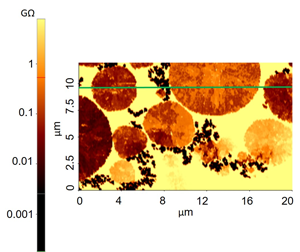
The qualitative and quantitative results acquired during these experiments are shown in Figures 3 and 4. Figure 3 presents the topography and electrical data measured in the sample. The topography image (Figure 3A) shows that the sample surface consists of circular-shaped plateaus with diameters ranging from 2 to 8 µm. The circular plateaus with brighter colors represent areas with greater height, whereas the areas with darker color represent low-lying areas. The resistance image (Figure 3B) features brighter-colored areas that represent higher surface resistivity, whereas areas with darker colors represent lower surface resistivity. The darker colors on the conductance image (Figure 3C) represent areas with lower surface conductivity, whereas brighter colors represent higher conductivity. When comparing topography and resistance images, one can easily observe that higher circular plateaus have lower resistance when compared to low-lying areas. Comparison of the topography and conductance images demonstrates that circular plateaus with higher height have higher conductance when compared to low-lying areas. This can also be observed in the 3D-overlay image of topography and conductance (Figure 3D) acquired in the XEI mode. Both resistance and conductance images show a clear picture of the small grains surrounding the circular plateaus. It was discovered that these small grains have lower resistivity and higher conductivity when compared to the circular plateaus. Analysis of the corresponding line profile (Figure 3E) of the topography, conductance, and resistance images confirms that the circular plateaus are regions with the highest height (approximately 50–60 nm). On the other hand, low-lying areas possess highest resistivity (approximately 8 GΩ). The line profile of the conductance image shows that the small grains around the circular plateaus are regions with the highest conductivity (approximately 1.3 μS).

Figure 3: Topography (A), resistance (B), and conductance (C) images acquired from an LIB electrode sample. Line profile (D): Topography line profile (red line, y-axis on left), resistance line profile (green, y-axis on right), and conductance line profile (blue line, y-axis on right). 3D-overlay image of topography and conductance (E).
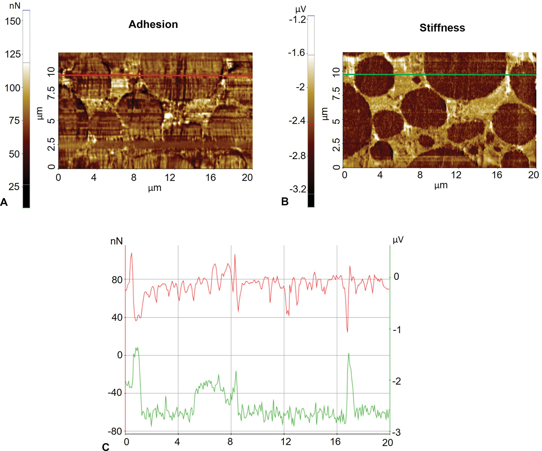
Figure 4: Adhesion (A) and stiffness images (B) acquired from an LIB electrode sample. Line profile (C): Adhesion line profile (red line, y-axis on left) and stiffness line profile (green, y-axis on right).
Figure 4 shows the mechanical data measured from the sample. The adhesion image does not show significant variations between the plateaus (Figure 4A). In the stiffness images, the brighter areas represent a surface with lower stiffness and modulus, whereas the darker areas correspond to the surface with higher stiffness and modulus (Figure 4B). A tendency toward higher adhesion is observed between the plateaus. The average adhesion force was measured to be 80 Nn (Figure 4C). The stiffness image shows noticeable stiffness variations in the sample surface. The measured stiffness value of the circular features represented by the dark color map was approximately -2.8 μV (note that the stiffness unit given here is qualitative data for comparative purposes and does not represent an absolute physical unit value of stiffness), whereas the areas represented by the bright color map were in a range from -1.5 to -2.0 μV.
Conclusion
A LIB electrode was successfully characterized by the Park NX-Hivac system using PinPoint™ SSRM. The data collected in this experiment demonstrate that this technique is an effective means for measuring the quantitative and qualitative topographical, electrical, and mechanical data of advanced materials with improved image quality and data accuracy. Overall, the PinPoint™ technique used in this study will greatly help researchers and device engineers in understanding the electrical and mechanical behavior of certain materials, such as LIB electrodes, that have unique properties.


