


Editor's Note: This article describes a method that received the Microscopy Today Innovation Award in 2011.
Introduction
Electrochemical and electrocatalytic phenomena underpin a broad spectrum of energy, chemical, and information technologies. Examples range from electrocatalytic activation of oxygen reduction reactions in fuel cells [Reference Ormerod1], gas-solid reactions, and ionic transport in gas sensors and oxygen pumps, to a wide gamut of electrochemical and transport phenomena in primary and secondary batteries [Reference Whittingham2]. Equally important is the role of ionic phenomena in information technologies, as exemplified by a recent wave of interest in memristive and electroresisitive information storage and logic devices [Reference Strukov, Snider, Stewart and Williams3, Reference Waser and Aono4]. This article examines a new type of scanning probe microscopy (SPM), referred to as electrochemical strain microscopy (ESM), that can provide a better understanding of these complex phenomena.
Interfaces and structural defects. Common for solid-state electrochemical systems is the extreme complexity of underpinning mechanisms that typically include interplay between electronic and ionic transport, gas-solid and interfacial electrochemical reactions, and long-range strain fields [Reference Adler5]. In solids, these processes are sensitively affected by the presence of interfaces and structural defects, which can act as preferential pathways or blocks for electronic and ionic transport, and nucleation centers for phase transformations. Hence, structural defects control operation, failure mechanisms, and lifetime of devices. The length scales are the nanometer and atomic scales of individual structural defects, submicron Debye lengths that control screening of electrostatic interactions, or micron-scale utilization lengths determined by interplay of diffusivities and reaction rates.
Electrochemical phenomena. New understanding of the electrochemical and electrocatalytic phenomena in solids can be achieved when these processes can be probed on the length scale of individual morphological features and atomically defined structural defects. When available, this knowledge will tie macroscopic functionality to atomic-scale mechanisms, paving the way for knowledge-driven materials design and optimization. The recent breakthroughs in understanding the kinetics and thermodynamics of macromolecular reactions on a single molecule level enabled by the molecular force spectroscopy techniques [Reference Rief, Oesterhelt, Heymann and Gaub6] are an example of such progress.
Field confinement. The key aspect of solid materials is that the defects are defined relative to the corresponding crystallographic lattice and, unlike molecules, cannot be “isolated.” The traditional nanoscience approach of matter confinement in the form of nanoparticles, wires, or thin films is also limited, because newly created surfaces will also act as defects. The alternative approach for probing a material's functionality is to use field confinement. In the latter, the SPM tip focuses an electric or thermal field in a nanometer-scale region of material, inducing local transformations. In parallel, the measured current or force signal provides information on processes in the material induced by local stimulus. The uniqueness of this approach is that a transformation can be probed in material volumes containing no or single individual extended defects, paving a pathway for studying phase transformations and electrochemical reactions on a single-defect level [Reference Kalinin, Jesse, Rodriguez, Chu, Ramesh, Eliseev and Morozovska7].
In this article we summarize the principles and recent applications of electrochemical strain microscopy [Reference Balke, Jesse, Morozovska, Eliseev, Chung, Kim, Adamczyk, Garcia, Dudney and Kalinin8, Reference Kumar, Ciucci, Morozovska, Kalinin and Jesse9], the recently developed technique for probing electrochemical transformations in solids. We also discuss applications of ESM for probing reversible and irreversible electrochemical reactions, as well as future combined ESM-electron microscopy methods for probing associated atomistic mechanisms.
Probing Reversible Electrochemical Processes
Application of voltage bias to an SPM tip in contact with a surface often produces (irreversible) electrochemical reactions in the form of local oxidation or electrochemical damage. These phenomena were documented in the early days of SPM as a detrimental factor for SPM operation. In the mid-1990s, it was recognized that SPM-based electrochemistry could be a powerful tool for nanostructure fabrication, with examples ranging from nanooxidation of metals and semiconductors to the formation of metallic structures on solid-state ionics to deposition of semiconductors or carbon from suitably chosen gas or liquid electrolytes [Reference Garcia, Martinez and Martinez10]. The characteristic aspect of tip-assisted electrochemistry is that extremely high fields in the tip-surface junction, reaching 107−109 V/m, can induce non-standard electrochemical behaviors, including the formation of carbon from CO2 [Reference Garcia, Losilla, Martinez, Martinez, Palomares, Huttel, Calvaresi and Zerbetto11] or SiC from SiO2/Si and hexane [Reference Garcia, Martinez and Martinez10].
The onset of irreversible electrochemical processes, for example, formation of metal or semiconducting nanoparticles or local growth of oxide, can be readily detected from comparison of surface topographic images before and after modification, or other chemical or structural probes (for example, microRaman). However, it is also of interest to probe the reversible electrochemical transformations, for example, the reversible motion of ions in a battery or fuel cell device. Also of interest are reversible changes accompanying or preceding irreversible processes, for example, vacancy accumulation prior to precipitation of the second phase inclusion. This requires the electrochemical process to be probed during the application of a bias to the tip, ideally in the form of voltage or time spectroscopies that offer nanoscale analogs of classical electrochemical methods. Implementation of these methods necessitates appropriate measurable signals linked to the local ionic concentration.
One approach for probing local electrochemistry can be based on local current detection, effectively transitioning macroscopic electrochemical measurement strategies to the nanoscale. Electronic conduction currents can indeed provide indirect information on tip-induced electrochemical transformations, for example, local oxidation of the surface will be associated with increase of resistivity. However, the Faradaic current related to the extent of an electrochemical process does not offer a readily measurable signal! Indeed, measurements at ~pA levels over ~1 s timeframes correspond to electrochemical transformations in (0.1–1 μm)3 of material, well above the tip-surface contact radius of SPM (3–10 nm). Thus, electrochemical transformation at high resolutions cannot be probed through current detection. Paradoxically, in an irreversible process a particle of newly formed material can be detected by SPM long before the associated Faradaic current can be measured [Reference Arruda, Kumar, Kalinin and Jesse12].
ESM uses an alternative approach for electrochemical detection based on the intrinsic link between the concentration of ionic species and molar volume of the material [Reference Balke, Jesse, Morozovska, Eliseev, Chung, Kim, Adamczyk, Garcia, Dudney and Kalinin8, Reference Kumar, Ciucci, Morozovska, Kalinin and Jesse9]. Here, an application of electric bias to an SPM tip results in redistribution of mobile ions under the tip and, hence, strain and local surface displacement, which is registered by the photodetector (Figure 1). The sensitivity of standard SPM platforms allows for detection of 2–5 pm surface displacements in the ~0.1–1 MHz frequency range. For the case of a Li-ion battery, one can estimate detection limits corresponding to ~20 percent change in lithiation state within 1 unit cell for materials such as LiCoO2 (the most classical cathode component in Li-ion batteries). This is a 6–8 order-of-magnitude reduction in probing volume as compared to classical electrochemical strategies based on Faradaic current measurements.
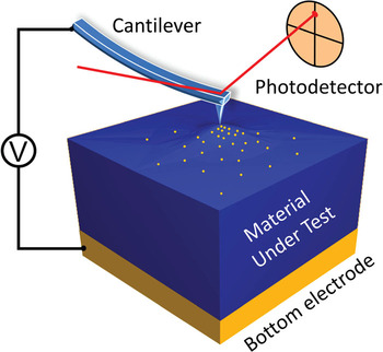
Figure 1: Schematics of ESM measurement technique. Application of bias to the tip of a conductive cantilever results in ionic motion under the tip and related local volumetric changes in the material under test that are registered by the photodetector.
Imaging mode. The operation of ESM in imaging mode is illustrated in Figure 2. The characteristic aspect of many electrochemical systems is extreme surface roughness concomitant with high electrochemical activity, as visible in the deflection atomic force microscopy (AFM) image of the polycrystalline LiCoO2 sample (Figure 2a). To obviate the effect of surface roughness on measured signal due to indirect topographic cross-talk [Reference Jesse, Guo, Kumar, Rodriguez, Proksch and Kalinin13], the measurements are performed in band excitation mode (BE) [Reference Jesse, Kalinin, Proksch, Baddorf and Rodriguez14]. In BE, the cantilever is excited with a chirp AC voltage pulse, and response is detected in a band of frequencies chosen to contain contact resonance, equivalent to parallel detection of response at multiple frequencies. This allows a decoupling of the amplitude of the response (measure of electrochemical activity) and resonance frequency of the cantilever (measure of surface stiffness and topography). The amplitude of the response on vertical and torsional cantilever resonances can then be mapped as the maps of the out-of plane (OP) and in-plane (IP) ESM signal in Figures 2b and 2c. This measured electromechanical signal, that is, amplitude and phase of surface response to electric bias applied to the tip, is determined by the diffusion and chemical expansion (Vegard) tensors of material and hence is the measure of local electrochemical activity [Reference Chung, Balke, Kalinin and Garcia15]. Figure 2d illustrates the typical variation of the ESM signal across the surface in the form of a 2D spectrogram that plots response versus position along the surface and frequency. The amplitude-frequency curves in Figure 2e illustrate responses at single spatial locations.
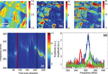
Figure 2: (a) Surface deflection, (b) out of plane, and (c) in-plane ESM amplitude images of LiCoO2 surface. Also shown (d) is 2D frequency spectrogram obtained across the marked line in (b). Several resonance frequency curves obtained at different points in (d) are also shown in (e). Samples courtesy of Nancy Dudney (ORNL).
During this process the tip can strongly affect the state of the surface. This behavior is demonstrated in Figure 3, illustrating the deflection image and ESM map of a different region on the LiCoO2 surface. Note the presence of a highly active grain during the first scan. During the second scan, the grain has disappeared (only inactive grains remain), and surface topography now shows the presence of debris particles. Presumably, the ESM excitation triggered a runaway electrochemical process in this grain that led to its chemical decomposition.
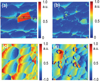
Figure 3: ESM amplitude (a, b) and frequency (c, d) images of LiCoO2 surface before (a, c) and after (b, d) measurements showing that excessive electrochemical activity induced in active grains by ESM can electroform them. Sample courtesy of Nancy Dudney (ORNL).
Spectroscopy modes. The ESM can be extended to a broad spectrum of time and voltage spectroscopies. In these, the ESM signal is probed as a function of bias: during a triangular sweep or as time after application of the bias pulse of constant or variable magnitude. These spectroscopic measurements can be taken over a dense grid of points, giving rise to 4D and 5D spectroscopic imaging techniques. The simple case of bias spectroscopy is illustrated in Figure 4 for ESM hysteresis loop measurements on a Pt particle on a yttrium-stabilized zirconia surface. The signal in this case is related to the oxygen reduction/evolution reaction on the sample surface and shows strong enhancement at the boundary between the catalytic particle and the yttria-stabilized zirconia electrolyte.
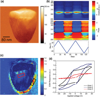
Figure 4: (a) Surface topography of Pt nanoparticle on Yttrium stabilized zirconia surface (sample courtesy of Phil Rack, UTK). (b) Characteristic 2D spectrogram representing the ESM amplitude as a function of time for triangular bias sweep at a selected location. This data set can be analyzed to give rise to ESM hysteresis loops that are acquired at each sample location. (c) Map of the hysteresis loop area and (d) hysteresis loops for several specific locations.
Probing Irreversible Electrochemical Processes
Although the operation of fuel cells and batteries is underpinned by reversible electrochemical processes, of a strong interest are irreversible electrochemical processes. Examples include formation of solid-electrolyte interfaces in batteries, formation of conductive channels in memristors, and processes underpinning degradation and failure of energy storage and conversion devices. Furthermore, operation of many battery types (most notably metal-air systems) is associated with significant charge-discharge hysteresis. Hence, understanding the life times and efficiency of energy systems necessitates probing irreversible electrochemical processes.
In this case, direct application of ESM time and voltage spectroscopic imaging modes is limited because the onset of reaction at a specific location precludes further measurements at the same location and its vicinity. To extend ESM to these phenomena, we have implemented the spectroscopy based on the resonance frequency shift detection during first order reversal curves measurements (FORC) [Reference Arruda, Kumar, Kalinin and Jesse12, Reference Guo, Ovchinnikov, Curtis, Johnson, Jesse and Kalinin16], as illustrated in Figure 4. The surface topography of the Li-ion glass ceramics (LICGC) after application of bias pulses shows the regular array of nanoparticles formed at the location of each pulse (Figure 5). The electrochemical activity varies across the sample surface—for example, at some locations particles are not formed. Although hysteresis loops cannot be measured in this case, detection of resonance frequency provides a readily measurable signal related to phase formation. Note that for negative polarity of the waveform, the jumps in resonance frequency correspond to nucleation of a particle below the tip. For positive bias (no electrochemical reaction) no frequency jumps are observed. The voltage corresponding to the jump in resonant frequency provides a measure of potential required to nucleate a particle on the surface at a preselected location and can potentially be used for high-resolution mapping.
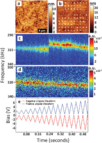
Figure 5: Surface topography of Li-ion conductive glass-ceramics (a) prior to and (b) after application of a series of bias pulses on a square grid. Parts (c) and (d) show evolution of the response (vertical axis: frequency, horizontal axis: time) during application of first order reversal curve waveform. For (c) the negative polarity of the jump in resonance frequency is associated with the nucleation of a Li particle below the tip. For (d) positive polarity, no jumps are observed, and drift in resonant frequency is presumably associated with Li-ion depletion below the probe. Shown also in (e) are the positive and negative FORC waveforms.
Application of ESM for reversible and irreversible processes in memristive materials is illustrated in Figure 6. In TiO2 memristive material, redox processes including oxygen vacancy formation and movement play a role in operational mechanisms, such as electroforming and its subsequent switching. Shown in Figures 6a–6c are reversible electrochemical processes in TiO2 thin films. Even though the hysteresis loop areas of Figure 6b are locally varied due to the polycrystalline features, there is no surface deformation after application of a series of bias pulses, and it shows a distinct ESM hysteresis loop opening. The absence of surface deformation and the presence of an ESM hysteric behavior clearly show reversible electrochemical activity related to the oxygen reduction/evolution reaction.
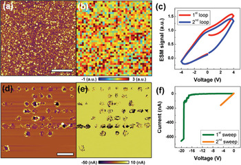
Figure 6: Reversible (a, b, c) and irreversible (d, e, f) electrochemical processes in memristive materials: (a) Surface topography after application of a series of bias pulses on a square grid (40 × 40), (b) spatial map of ESM hysteresis loop area, and (c) reversible average hysteresis loops in 25 nm-thick polycrystalline TiO2 thin films. Part (d) surface topography, (e) current map under −2 V after application of a series of bias pulses on a square grid (10 × 10), and (c) representative single point I-V sweeps in 30 nm-thick amorphous TiO2 thin films. The current map and I-V sweeps were carried out with 30 MOhm series resistor to avoid complete electrical breakdown. The first bias sweep of (f) is to generate electroforming state, and the second bias sweep of (f) is to confirm its electrical state. Scale bar is 4 μm. Sample courtesy of Woo Lee at Korea Research Institute of Standards and Science (KRISS), Korea.
Under the low bias sweeps (Figure 6c), which are far lower than electroforming bias, the oxygen reduction/evolution reaction reversibly occurs underneath the SPM tip. However, the irreversible electrochemical process can occur because of vacancy ordering once the applied bias exceeds a critical bias, the so-called electroforming bias. After the electroforming procedure, significant topographic change was observed in these areas as shown in Figure 6d. While the “blob” shape of the topographic change is seen in the Li-ion conductors of Figure 4b, the “volcano” shape of topographic change is seen in the TiO2 thin films of Figure 5d. Because oxygen gas bubbles escape from underneath the films under application of negative bias to the sample surface, a volcano shape of topographic change can be formed in these materials. As shown in Figures 6e and 6f that compare created topographic defects and conductivity in them, the irreversible electroforming process leads to electrically conductive states that are relevant to oxygen vacancy ordering.
Toward Atomic-Level Probing of Electrochemical Reactions
The ESM measurements allow the probing of reversible and irreversible electrochemical reactions on the sub-10 nm scale, approaching the level of individual extended structural defects. Of obvious interest is the collection of atomic-level structural information of the defect so that functionality and structure are correlated directly, as was recently demonstrated for ferroelectric materials [Reference Rodriguez, Choudhury, Chu, Bhattacharyya, Jesse, Seal, Baddorf, Ramesh, Chen and Kalinin17].
The progress in this direction will come with the combination of local SPM excitation with focused X-ray and (scanning) transmission electron microscopy probes, (S)TEM. This approach was recently demonstrated for ferroelectric domain switching in pioneering work by Chang [Reference Chang, Kalinin, Yang, Yu, Bhattacharya, Wu, Balke, Jesse, Chen, Ramesh, Pennycook and Borisevich18] and subsequently by Nelson et al. [Reference Nelson, Gao, Jokisaari, Heikes, Adamo, Melville, Baek, Folkman, Winchester, Gu, Liu, Zhang, Wang, Li, Chen, Eom, Schlom and Pan19]. The possible scenarios for these studies are illustrated in Figure 7. Specifically, (S)TEM can be used to examine the irreversible transformations induced locally by an SPM tip. In this case, static surface deformations (or other fiduciary marks) are used to locate a modified region in the focused-ion beam (FIB) apparatus, and a lamella is milled out of the modified and non-modified regions and subsequently examined by (S)TEM, as shown in Figure 7a. Alternatively, the nanostructure can be fabricated prior to SPM modification, as shown in Figure 7b. The reversible processes can be studied using a combined SPM-STEM approach, in which case the reaction is induced locally by an SPM tip within the imaging region of STEM. Finally, pre-thinned structures can be fabricated, as shown in Figure 7d so that the constriction in which a reaction is observed is directly observable by (S)TEM.
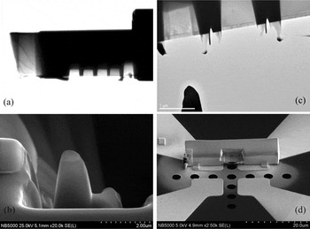
Figure 7: Possible paradigms for nano- and atomic-level electrochemical studies. Shown are (a) ex-situ examination of SPM-tip induced irreversible electrochemical reactions identified through FIB-milling, (b) ex-situ examination of SPM induced reaction in pre-milled nanoscale structures, (c) in-situ probing of reversible and irreversible processes using the STEM-SPM approach, and (d) in-situ probing of reversible and irreversible approaches using FIB-prepared thinned device structures.
Conclusion
ESM based on electromechanical detection is a new paradigm in scanning probe microscopy, beyond electronic current detection in scanning tunneling microscopy and force detection in AFM and related techniques. To date, ESM has been demonstrated for a broad variety of Li-ion cathode and electrolyte materials and oxygen conductors, at sub-10 nm resolution. The ESM technique can be extended to a broad range of time and voltage spectroscopies, enabling local characterization of electrochemical functionality in solids. Future work will involve implementation of ESM in liquid environments germane to Li-ion battery operation and elevated temperatures/reactive gases for fuel cell work. The combination of ESM with in-situ (S)TEM methods holds the promise of understanding electrochemical activity on a level of single atomically defined defects.
Note: The ESM imaging and spectroscopy techniques are currently available for the user community through the DOE user program. Additional information is available at www.cnms.ornl.gov.
Acknowledgments
Research supported (SVK, AB, YK, DL, AT) by the U.S. Department of Energy, Basic Energy Sciences, Materials Sciences and Engineering Division and partially performed at the Center for Nanophase Materials Sciences (SJ, AK, NB, TA), a DOE-BES user facility.


