


Introduction
Identification and characterization of materials with nanoscale resolution has always been the ultimate goal in atomic force microscopy (AFM). This knowledge is essential for correlating the macroscopic properties and performance of materials such as biomembranes or organic photovoltaics with their nanoscale inhomogeneity. Infrared spectroscopy is a standard technique for identification of materials, but its spatial resolution is limited by diffraction. Scattering scanning near-field optical microscopy (s-SNOM) in the infrared spectral region is an AFM-based technique that overcomes the diffraction limit and provides non-destructive, surface-sensitive chemical identification with a spatial resolution down to 10 nm [Reference Keilmann and Hillenbrand1,Reference Atkin2]. Standard AFM tapping mode operation is inherent to s-SNOM, which renders this technique well suited for soft materials where contact mode could cause tip and sample damage. Even more advantageous, as implemented in Bruker’s Inspire system for the first time, s-SNOM can be combined with PeakForce Tapping. In this article, we discuss new opportunities this affords for correlated and simultaneous nanochemical, nanomechanical, and nanoelectrical measurements on soft polymeric samples. Additional applications of the Inspire system are not covered here, for example, imaging of local strain [Reference Huber3,Reference Bensmann4], nano-antenna modes [Reference Olmon5,Reference Alonso-Gonzalez6], graphene plasmons [Reference Fei7,Reference Chen8], boron nitride phonon polaritons [Reference Dai9,Reference Xu10], phase-transitions [Reference Liu11] and biomaterials [Reference Brehm12–Reference Amenabar14].
Materials and Methods
Model polymer example
Designing novel material properties of polymer blends used, for instance, in organic photovoltaics or liquid crystals requires the ability to characterize the system at the nanoscale in order to correlate phase distribution with macroscopic performance. Figure 1 presents an example of an inhomogeneous, nanoscale polymer system, the model system poly(styrene-block-methyl methacrylate) (PS-b-PMMA). Panel (a) shows the topography of the 50 nm spin-cast thin film, an image unable to answer the question of whether the two components PS and PMMA coexist as a homogeneous mixture or phase-separated. We note that conventional tapping mode routinely provides topography information while preserving soft samples such as polymers. PeakForce Tapping, discussed below, can additionally inform us on a quantitative level about certain material properties, such as the modulus, and is preferred for imaging of the most delicate samples, such as DNA [Reference Slade and Hu15] or cells [Reference Pittenger16]. Identifying chemistries and phases by means other than their sometimes-unknown nanomechanical properties is often desired. Infrared spectroscopy is able to provide valuable information on the chemical composition because many materials show a unique fingerprint in the infrared spectral range. However, conventional far-field techniques such as Fourier-transform infrared (FTIR) spectroscopy are limited in spatial resolution to approximately half of the employed wavelength, that is, typically at least 10 μm in the fingerprint region and much larger than the 30–50 nm diameter of grains in Figure 1a. On the other hand, s-SNOM is a well-established near-field infrared technique that can overcome the far-field diffraction limit, allowing an improvement in spatial resolution by three orders of magnitude down to 10 nm.

Figure 1 Example polymer analysis. (a) Topography of a spin-cast, 50 nm thin PS-b-PMMA block copolymer film on Si substrate. (b) Corresponding nanoscale absorption at the 3rd harmonic obtained with Inspire at 1725 cm-1. At this frequency the infrared light resonantly excites the carbonyl C=O stretch that is only present in PMMA. Consequently, only the PMMA domains appear bright while PS does not absorb in this frequency range. A trench outside the displayed image and accessing the Si substrate was used as a reference material. The yellow dotted line marks the position of the line profiles for topography and IR absorption presented in (c) and (d), respectively. No correlation between the height in (c) and the absorption in (d) is found, indicating that the absorption image maps the nanoscale chemistry rather than topography artifacts. The step in absorption at a position of 260 nm has a width of 15 nm and represents a measure for the obtained spatial resolution that is limited by the tip radius of < 25 nm.
Applying s-SNOM imaging to the block copolymer sample reveals the quasi-lamellar PMMA domains in Figure 1b. These domains are detected by probing the carbonyl resonance at 1725 cm-1 that is present in PMMA but not in the PS chains. The height distribution does not correlate with the PMMA distribution, as can be seen from the line profiles taken along the yellow line in Figure 1b and extracted in Figure 1c for height and Figure 1d for IR absorption. Consequently, the absorption channel only probes the chemical composition and not topography artifacts. For the present example, the Pt-Ir metallized AFM probe had a nominal tip radius less than 25 nm. A spatial resolution of <15 nm can be estimated for the chemical mapping from the step in the line profile of Figure 1d at the position of 260 nm, in an area of minimal topography changes to rule out crosstalk with topography. We note that a spatial resolution in the IR of < 15 nm can be achieved without special tip/sample preparations, and the avoidance of tip/sample damage in tapping mode (vs. contact mode) results in highly reproducible results during multiple scans. This resolution is comparable to the tip radius due to strong confinement of the interaction volume by the exponential decay of the near-fields with distance and the field enhancement at the tip apex as discussed below. It has been shown before that tips with smaller radius of 10–15 nm allow for an even higher IR spatial resolution down to 8 nm [Reference Raschke17].
The s-SNOM mode
In s-SNOM, as implemented in the Inspire system, scattered light from an AFM tip is detected. Infrared light from a laser source, for example, from a continuous wave quantum cascade laser, is focused onto the end of a metallized AFM tip. Figure 2a shows the schematic of the AFM tip in an asymmetric Michelson interferometer that is used for near-field amplitude and phase image extractions. The infrared light incident on the tip is polarized along the tip in order to efficiently couple the electric field to a “nanoscale antenna” that gets polarized. The metal coating of the tip results in a lightning-rod effect for the incident light, that is, field concentration at the apex of the tip [Reference Bouhelier18]. Brought into contact with a sample, the exponentially decaying evanescent fields at the tip apex result in a local sample polarization according to the optical constants of the material. The sample polarization in turn influences the tip polarization and eventually the tip, as a nano-antenna, couples the polarization as radiation into the far-field. In other words, the tip elastically scatters the light, and this scattered radiation now contains information on the local dielectric properties of the sample under the tip with a spatial resolution given in first order by the radius of the tip, typically ~10–25 nm. The radiation is then collected by the focusing element, for example, a lens or parabolic mirror, followed by analysis in a Michelson-type interferometer.
Figure 2 Infrared signal acquisition. (a) Schematic diagram of the s-SNOM implementation in Inspire. Light from an infrared laser source is split into a reference beam that is reflected from a motorized mirror and a sample beam that is focused on an AFM tip. Backscattered light from the tip is detected with a MCT detector where it interferes with the reference light. In two-phase homodyne detection the reference mirror is set to two positions that allow phase-sensitive measurements to extract absorption and reflection data with nanoscale spatial resolution. (b) Schematic of the AFM tip illustrating the confinement of near-field signals E nf to small tip-sample distances compared to background signals E b. (c) Highly nonlinear decay of the near-field signal with height above the sample in contrast to the linear background signal allows extraction of the near-field contribution via tapping mode operation. The harmonic background signal in time can be distinguished from the anharmonic near-field signal by Fourier transformation. Detection at higher harmonics (2, 3, 4…) of the tip oscillation frequency allows suppression of the background signal.
Signal and background
The near-field scattering signal of the s-SNOM is usually buried in a much larger background scattering signal that does not contain the desired, sample-specific localized information. The background signal originates from scattering off the tip, the cantilever, and the sample surface because the focus of the incident light is still diffraction-limited to a few tens of micrometers. Despite its larger magnitude compared to the near-field signal, suppression of the background and subsequent near-field extraction turns out to be straightforward. The most common scheme is based on modulating the tip-sample distance, which conveniently corresponds to standard tapping mode AFM operation. The near-field signal increases strongly nonlinearly close to the sample surface, while far-field scattering shows only a linear signal versus distance dependence, as shown in Figures 2b and 2c. Consequently, the harmonic motion of the AFM tip in tapping mode at the cantilever resonance frequency Ω results in a background signal that varies only slightly with Ω, while the near-field signal shows higher harmonics nΩ (with integer n ≥2). Typically, near-field signals are acquired at the second or third harmonic of the cantilever resonance frequency, with good background suppression where the tapping frequency Ω is tens to hundreds of kilohertz at a typical probe oscillation amplitude of several tens of nanometers.
Signal analysis
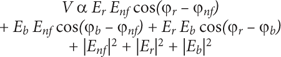
To enhance the weakly scattered near-field signal of the s-SNOM and to obtain the electric field and the phase of the scattered light, an asymmetric Michelson-type interferometer is employed. This technique represents a straightforward way to obtain the near-field absorption and reflection signals, the nanoscale analogs of conventional far-field FTIR absorption, and reflection signals. A typical configuration for such a homodyne detection scheme is depicted in Figure 2a. The light of the infrared light source is split with a 50:50 beamsplitter to provide a reference beam that is reflected from a piezo-controlled mirror and then focused on a mercury cadmium telluride (MCT) detector together with the scattered light from the AFM tip. The recorded interference signal on the detector V contains the near-field amplitude and phase, E nf and φ nf respectively, and the corresponding values for the reference (E r, φ r) and the background signals (E b,, φ b) in the following way:
 $$\eqalignno{ & V\propto E_{r} {\rm }E_{{nf}} \cos (\varphi _{r} {\minus}\varphi _{{nf}} ){\plus}E_{b} E_{{nf}} \cos (\varphi _{b} {\minus}\varphi _{{nf}} ){\plus}E_{r} E_{b} \cos \left( {\varphi _{r} {\minus}\varphi _{b} } \right) \cr & {\plus}\,\mid\,E_{{nf}} \,\mid\,^{2} {\plus}\,\mid\,E_{r} \,\mid\,^{2} {\plus}\,\mid\,E_{b} \,\mid\,^{2} \cr} $$
V α Er Enf cos(ϕr – ϕnf) + Eb Enf cos(ϕb – ϕnf) + Er Eb cos(ϕr – ϕb) + |Enf|2 + |Er|2 + |Eb|2This equation can be simplified to extract the desired near-field amplitude E nf and phase φ nf The last four terms are suppressed by signal demodulation or are negligible compared to the other terms, and the second term can be neglected because E r >> E b. We note that the weak near-field signal is enhanced in the first term by multiplication with the much larger reference field. To extract near-field amplitude and phase, a two-phase homodyne detection scheme is employed, that is, the signal is measured in two positions of the reference mirror corresponding to two distinct reference phases φ r. These mirror positions are adjusted with the SNOM tip over a non-absorbing, reflecting material in the infrared region of interest such as Si. In practice, the mirror is translated until a maximum of the demodulated detector signal is found, corresponding to a vanishing phase difference between reference and near-field phase on the Si material. Moving the mirror by 1/8 of a wavelength shifts the reference phase by π/2 and thus suppresses the detector signal entirely on the non-absorbing Si. After having defined the reference mirror positions in the described way, the SNOM tip is placed over the sample of interest. The detector now measures a signal Vrefl α Er Enf′ cos(ϕnf′) (1st mirror position) and Vabs α Er Enf′ sin(ϕnf′) (2nd mirror position), corresponding to signals proportional to the reflection and absorption of the sample, respectively [Reference Xu19–Reference Mastel21]. Note that these quantities represent the real and imaginary part of the complex near field Enf′ exp(iϕnf′) from which the amplitude and phase can easily be obtained.
We emphasize that for weak oscillators such as polymers or biomaterials the obtained absorption spectra allow material identification without the need for elaborate modeling. Different models exist ranging from those that allow a qualitative understanding to those that give a detailed, quantitative description of the tip-sample interaction [Reference Atkin2, Reference Cvitkovic22–Reference McLeod24]. However, the exceptional agreement of near-field absorption data and standard far-field FTIR data in the case of polymers or biomolecules has been shown recently in several publications [Reference Amenabar14, Reference Xu19–Reference Mastel21] and renders s-SNOM an excellent and modeling-free technique for most practical cases.
PeakForce Tapping mode
An AFM is the basis for s-SNOM operation, and hence s-SNOM can be combined with other AFM modes. PeakForce Tapping is such a mode, and it is particularly suitable for imaging of soft samples, such as polymers. In PeakForce Tapping, the tip-sample distance is modulated sinusoidally. The tip-sample interaction in contact is controlled to keep the maximum force or “peak force” constant. This method of precise control of the tip-sample interaction force captures and analyzes approach and withdraw curves at each pixel with 1–2 kHz repetition rate and at user-defined forces down to tens of pN [Reference Pittenger16]. One aspect of PeakForce Tapping is that its force feedback preserves the AFM tip and sample and thus enables imaging of delicate samples with ultra-high resolution. This allows, for instance, routine observation of the major and minor grooves in the DNA double helix [Reference Slade and Hu15, Reference Pyne25]. Another aspect is that force curves can be acquired and evaluated online during imaging to obtain mechanical properties of the sample in a quantitative way, including, for example, the modulus, adhesion, or the deformation [Reference Pittenger16, Reference Woods26, Reference Dover27]. In addition, PeakForce Tapping can be combined with potential or current measurements in PeakForce Kelvin probe force microscopy (PF-KPFM) [Reference Li28] and PeakForce tunneling AFM (PF-TUNA) [Reference Li29], respectively. This versatility is now further enhanced in Bruker’s Inspire by the addition of s-SNOM, allowing correlated, even simultaneous nanochemical, nanoelectrical, and nanomechanical data acquisition.
Results
Infrared detection of PMMA phase
As an example of the high chemical sensitivity of the s-SNOM technique, its spectral accuracy, and its ability to deliver easily interpretable data that corresponds to far-field spectra, we investigated a spin-casted PS-PMMA blend (70:30 ratio) on a Si substrate. Mapping of the PMMA distribution is shown in Figure 3a and 3b where nanoscale s-SNOM reflection and absorption data were acquired at different infrared frequencies. Figure 3c presents the topography with taller PMMA domains embedded in the PS matrix. The laser was tuned around the carbonyl resonance of PMMA. As outlined above, a non-absorbing reference is needed to set the reference mirror phase and obtain near-field absorption data. Conveniently, PS serves this purpose because it has a flat infrared response in the displayed frequency range. The absorption and reflection profiles (Figure 3d) were extracted on the PMMA domain from multiple images acquired at different, discrete frequencies. Both quantities exhibit a shape characteristic of a Lorentzian absorption line, as verified by fitting with the common Lorentz oscillator model (solid lines). We note that only recently the same repetitive imaging at discrete laser frequencies has been employed to sweep over the PMMA carbonyl resonance in a PS-b-PMMA block copolymer system [Reference Pollard30], similar to the one imaged in Figure 1. Both, absorption line center frequencies and line widths, were measured with 0.2 cm-1 spectral precision to resolve intermolecular Stark shifts of the carbonyl resonance occurring between the center and interface of the PMMA domains due to locally varying electric fields [Reference Pollard30]. That study and our data underline that near-field absorption on nanoscale systems is routinely obtainable, highly reproducible, and matches far-field data that allows material identification without the need for modeling of the exact tip-sample near-field interaction. Furthermore, it highlights the high chemical sensitivity and spectral accuracy consistently achievable with s-SNOM that makes it possible to analyze on a quantitative level the physics and chemistry of such minuscule effects as the Stark shift between polymer chains.
Figure 3 Analysis of a two-phase polymer. (a) S-SNOM reflection and (b) absorption signals at the third harmonic of a PS-PMMA blend with topography in (c). (a) and (b) show a constant reflection and vanishing absorption of the PS matrix for different infrared frequencies where the PS material with its flat, absorption-free dispersion serves as a reference material. On the contrary, the PMMA domains exhibit a distinct wavelength-dependent behavior, as extracted for the large domain in panel (d) for multiple frequencies. Both reflection and absorption can be fitted with a common Lorentz oscillator model (solid lines).
IR reflection and absorption in a biodegradable polymer
To emphasize the wide applicability of s-SNOM and its capability to provide additional information about sample properties, we turn to PHBV or poly(3-hydroxybutyrate-co-3-hydroxyvalerate), a biodegradable polymer. The topography of the PS-PHBV sample (ratio 70:30) obtained from spin-casting is presented in Figure 4a, and the corresponding nanoscale reflection and absorption in Figures 4b and 4c, respectively. The topography reveals two different morphologies: disk-like structures deeply embedded in a background matrix and an extended, island-like structure at the bottom right that is only slightly lower in height than the matrix. In panels 4b and 4c, the carbonyl group of PHBV is used to assign both morphologies in the topographic image to PHBV. Absorption and reflection behave similarly to the PS-PMMA example of Figure 3 with a resonance around 1720 cm-1. On resonance, darker, that is, less absorbing, boundaries are observed within the island-like structure. This might indicate incomplete phase separation with PS or could be related to a local difference in degree of crystallinity within PHBV. Clearly, s-SNOM uncovers that PHBV exhibits more heterogeneity than the topography image alone provides.
Figure 4 Analysis of a biodegradable polymer. (a) Topography of a PS-PHBV blend showing two morphologies: disk-like ones and an extended, island-like one at the bottom right, both embedded into the background matrix. (b) Nanoscale reflection and (c) absorption for different frequencies around the carbonyl vibrational mode. The PHBV phase is identified from resonant absorption mapping at 1720 cm-1 in (c). It occurs in the two different morphologies and exhibits some internal structure within the island-like region.
Simultaneous modulus and reflection mapping of a polystyrene-polyethylene blend
Because s-SNOM is an AFM-based technique, it can be supplemented and enhanced by AFM modes other than tapping mode [Reference Huang31]. Here, we demonstrate the combination of s-SNOM with PeakForce Tapping using a low-density polyethylene (LDPE) sample. LDPE is most commonly known from plastic bags. The topography of a PS-LDPE blend is displayed in Figure 5a. Modulus mapping in Figure 5b reveals soft disks within a stiff matrix of higher modulus. This contrast already identifies the high-modulus material as PS with a nominal 2 GPa modulus with embedded LDPE disks of 0.1 GaP modulus. This assignment and the topography data inform us that the softer LDPE disks protrude out of the surface by 10 nm. Both materials are not absorptive at the infrared frequency of 1880 cm-1, but Figure 5c reveals a clear contrast in the simultaneously acquired reflection channel. LDPE with a lower refractive index exhibits a lower near-field reflection signal compared to PS. This is an example where the nanoscale reflection information alone is sufficient to distinguish materials, a fact often used, for example, when studying metallic domains in insulator-to-metal transition materials [Reference Liu11]. In general, metals can be distinguished in this way from insulators, whereas phonon or plasmon resonances can result in resonant enhancement with signals exceeding that of metals [Reference Hillenbrand32].
Figure 5 Analysis of a polystyrene-polyethylene blend. (a) Topography of a PS-LDPE sample, (b) simultaneously acquired modulus, and (c) infrared reflection at 1880 cm-1. Lower modulus in (b) identifies the softer LDPE domains compared to the PS matrix. The reflection image in (c) confirms this assignment where LDPE with a lower refractive index in the flat region of its absorption-free dispersion exhibits lower near-field reflection.
Simultaneous modulus and absorption mapping of a contamination on a PS-PMMA film
In contrast to the previous example (Figure 5), we will turn to a system where topography, modulus, and reflection information are not sufficient to characterize the sample, but where IR absorption properties need to be measured as well. The combination of IR and mechanical data was demonstrated on the previous PS-PMMA blend, examined in Figure 3. The topography (Figure 6a) reveals taller PMMA domains in a PS matrix, similar to what was observed in Figure 3. The highest feature in the image however, located close to the image center, exhibits less internal structure than the PMMA domains that also protrude from the surface. From topography information alone, it is unclear whether this feature is PMMA or a contamination. Its corresponding modulus mapped in Figure 6b appears to lie between the one measured for PMMA and PS. Adding IR reflection data (Figure 6c) does not solve the puzzle: the reflection acquired at 1728 cm-1 resonant with the PMMA absorption (compare with Figure 3d) shows a PMMA-like signal for the feature. So far the topography, modulus, and reflection signals are ambiguous. This underlines the need for additional IR absorption data (Figure 6d), which reveals a vanishing absorption similar to that of PS for the tall feature observed in topography. Combining reflection and absorption data, we learn that the dielectric properties of the contamination must be different from PS and PMMA, and hence a contamination of some sort must be present.
Figure 6 Analysis of a contaminated PS-PMMA film. Simultaneously acquired (a) topography, (b) modulus, (c) IR reflection, and (d) absorption. IR reflection and absorption were measured for a laser frequency of 1728cm-1, tuned to the C=O vibrational mode characteristic of PMMA and absent in PS. While topography, modulus, and reflection cannot unambiguously identify the nature of the tallest feature in topography (close to the image center), the combination with IR absorption establishes it to be neither PS, nor PMMA, but some sort of contamination.
Discussion
In this paper we have introduced the underlying working principles of Bruker’s Inspire system and its application to polymers for imaging chemical phases. The presented s-SNOM technique based on short-range near-field interaction shows much higher spatial resolution in the infrared fingerprint region than diffraction-limited, far-field infrared spectroscopy. A PS-b-PMMA block copolymer system (Figure 1) served to demonstrate a spatial resolution down to 10–20 nm in agreement with previous publications [Reference Keilmann and Hillenbrand1, Reference Atkin2, Reference Raschke17]. In this model system PMMA domain sizes of 30–50 nm were measured, a similar size as recently published [Reference Pollard30]. AFM topography and chemical material distribution deduced from s-SNOM were shown not to correlate in this sample, a fact that underlines the necessity for nanoscale chemical identification. The chemical specificity was presented using a vibrational resonance in a different, phase-segregated PS-PMMA film (Figure 3). Resonantly driving the carbonyl mode that is present in PMMA but not in PS allowed to unambiguously identify the PMMA domains. Off resonance, the contrast between PS matrix and PMMA domains vanished. Both absorption and reflection properties extracted via s-SNOM exhibited the expected line profile of a Lorentz oscillator [Reference Pollard30], highlighting the chemical specificity, but also the modeling-free data interpretation that renders s-SNOM so valuable for applications.
As another example we imaged PHBV (Figure 4). Here, s-SNOM could map the PHBV domains in the PS matrix and additionally resolved structures within single PHBV domains that possibly result from incomplete phase separation or varying degrees of crystallinity. These features were hard or impossible to resolve in AFM topography alone. Mapping of the non-resonant reflection properties of a PS-LDPE blend (Figure 5) demonstrated that imaging in an absorption-free region can be employed to identify materials on the nanoscale as well.
S-SNOM as an AFM-based technique can be further enhanced by combining it with other versatile AFM modes. Two examples of correlative nanooptical and nanomechanical mapping were given (Figure 5 and 6); this combination of s-SNOM with PeakForce Tapping is expected to have many interesting applications. Not only can the nanomechanical properties be mapped, but PeakForce Tapping enables either amplitude modulation or frequency modulation kelvin-probe force microscopy without the need to turn to tapping mode for feedback. In addition it enables high-resolution conductivity mapping in tunneling or conducting AFM without requiring contact mode for conductivity measurements, which is mandatory for soft or fragile samples. Hence, nanooptical, nanomechanical, nanoelectrical, and nanopotential experiments are now accessible, and, in the case of polymer science, this technology could be employed to correlate functionality and phase distributions in organic photovoltaics, fuel cells, conducting polymers, organic electronics, or liquid crystal films.
Conclusion
Functional polymer blends with smaller and smaller domain sizes require novel techniques such as s-SNOM to image their material distribution. S-SNOM as implemented in the Inspire tool can directly acquire the sample’s nanoscale absorption and reflection, thus providing easily interpretable, modeling-free IR data that can be compared to standard FTIR spectra. In combination with other AFM techniques, s-SNOM can be employed to simultaneously measure nanooptical, nanomechanical, and nanoelectrical properties, enabling correlated experiments to enhance our understanding and allow optimization of materials in various fields of polymer science.
Acknowledgments
The authors thank Bede Pittenger and Natalia Erina for sample preparation, and Greg Andreev for providing the data presented in Figure 5.

