Introduction
We demonstrate in this article an exciting new method for obtaining electron Kikuchi diffraction patterns in transmission from thin specimens in a scanning electron microscope (SEM) fitted with a conventional electron backscattered diffraction (EBSD) detector. We have labeled the method transmission EBSD (t-EBSD) because it uses off-the-shelf commercial EBSD equipment to capture the diffraction patterns and also to differentiate it from transmission Kikuchi diffraction available in the transmission electron microscope (TEM). Lateral spatial resolution of less than 10 nm has been demonstrated for particles [Reference Geiss, Keller and Read1, Reference Geiss2, Reference Keller and Geiss3] and better than 5 nm for orientation mapping of thin films [Reference Trimby4, Reference Brodusch, Demers and Gauvin5]. The only new requirement is a specimen holder that allows the transmitted electrons diffracted from an electron transparent sample to intersect the EBSD detector. We briefly outline our development of the technique, followed by descriptions of sample preparation techniques and operating conditions. We then present examples of t-EBSD patterns from a variety of specimens, including particles of diameter <10 nm, wires of diameter <80 nm, and films with thicknesses from ~5 nm to 300 nm. Finally, we discuss the phenomenon in the context of Monte Carlo electron scattering simulations.
History
The idea of using EBSD equipment to capture Kikuchi diffraction patterns in transmission from thin specimens came about as a consequence of being unable to reliably capture EBSD patterns in the usual reflection geometry from samples that lacked flat surfaces. For example, during attempts to measure strains in InGaN nanowires by EBSD image correlation [Reference Wilkinson, Dingley, Meaden and Schwartz6], we could not obtain high-quality patterns from many of the nanowires. This followed even though the nanowires were large enough (~80 nm) that spatial resolution should not have been a problem. Unfortunately, the surface facets of the hexagonal cross section nanowires were oriented at random angles relative to the EBSD camera. This led to specular scattering of the incident electron beam away from the camera and mostly produced patterns that were not of sufficient quality to use in image correlation.
Because the nanowires were dispersed on a transparent carbon substrate, we tried to obtain diffraction patterns using the same samples repositioned in such a way that the patterns would originate at the bottom surface of the nanowires from electrons that had transmitted through the sample. In this geometry the scattering from the surface facets of the nanowires should not compromise the quality of the resulting diffraction patterns. With the sample in this configuration, transmission Kikuchi electron diffraction patterns were obtained from almost every InGaN wire. Figure 1 shows an SEM image with a few clusters of nanowires dispersed on a carbon substrate, along with t-EBSD patterns obtained from the indicated locations. This was our first experimental demonstration of Kikuchi diffrac-tion patterns obtained in transmission using EBSD hardware in an SEM.

Figure 1: Secondary electron image of clusters of InGaN nanowires dispersed on an electron-transparent carbon substrate. Raw EBSD patterns, obtained in transmission from the indicated wires, are shown in the inserts. SEM operating conditions: 20 kV, 450 pA.
Methods and Materials
Validation of diffraction in transmission. To show that this was indeed a transmission phenomenon, we prepared a large-area continuous sputtered film consisting of 40 nm Ni on a 2.5 nm Ta adhesion layer deposited on a 40 nm Si3N4 window TEM substrate. Figure 2a shows the film as seen in TEM, revealing a grain diameter of 15 nm ± 4 nm. We were unable to obtain reflection EBSD patterns from the sample with the Ni film facing the detector (Figure 2b). However, by orienting the sample in the transmission geometry with the Ni film down, we obtained indexable patterns from every grain sampled (Figure 2c). The continuous nature of the film established that the patterns originated from transmitted electrons, and the appearance of single patterns demonstrated a spatial resolution of at least 15 nm. Note that the Ni t-EBSD patterns were obtained after the incident beam had passed through approximately 42.5 nm of amorphous material before entering the Ni.

Figure 2: Comparison of reflection and transmission EBSD patterns. (a) Bright-field TEM image showing ~15 nm grains of a nickel film; (b) EBSD pattern with the Ni film specimen in the conventional reflection geometry at 28 kV, yielding no recognizable pattern; (c) a well-defined t-EBSD pattern taken at 28 kV with the Ni film facing the EBSD camera.
Typical operating conditions. The microscope used in these experiments was a LEO 1525 FE-SEM, and the EBSD equipment was from TSL-EDAX. We have also obtained t-EBSD patterns with equipment from other microscope and EBSD vendors, as well as from microscopes with W-sources. We have obtained patterns at voltages between 10 kV and 30 kV with probe currents as high as 1.25 nA, which is the highest available on our system. Pattern definition was extremely weak for probe currents less than ~300 pA. With the sample positioned at a working distance of 4–6 mm, the pattern center is located at or just off the top of the phosphor screen of our EBSD detector. Even with this unusual geometry, the vendor-supplied software could be used to index the patterns. The indicated sample normal, reference, and transverse directions—ND, RD, and TD, respectively—are not correct, and differences must be accounted for when describing the orientation.
Sample preparation. To prepare particle and nanowire samples for t-EBSD, we pipette a drop of a dilute dispersed suspension of the particles, usually in ethanol, onto a thin carbon substrate, suspended on a conventional 3 mm diameter, 200 mesh Cu grid commonly used for TEM. We have also prepared nanowire samples by directly swiping a carbon grid over a substrate with protruding nanowires; the sample shown in Figure 1 was prepared in this manner. Thin metal films were prepared by directly sputtering or evaporating the metal onto transparent carbon or silicon nitride window substrates. Thin foils can also be prepared from bulk samples using standard methods of chemical, electrochemical, or FIB thinning. Almost any crystalline sample that is appropriate for TEM study is acceptable for t-EBSD.
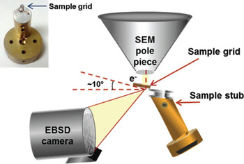
Mounting for t-EBSD. We mount the grids under a clip on a conventional 12.7 mm diameter SEM stub and raise the sample to give a working distance of 4–6 mm (Figure 3). We used an extension from the usual stage to raise the sample so that it could be tilted as shown in the figure, without interfering with the EBSD camera. To minimize shadowing from the specimen grid, noticeable in some patterns, we tilt the sample up to 20° from the incident beam normal; this also enables a simple coordinate transformation between the reflection and transmission configurations.

Figure 3: Sample holder used for positioning samples for t-EBSD in the SEM. The insert shows the actual hardware used.
Results
We demonstrate here results from a variety of particles with different atomic numbers and physical dimensions. Results are also presented from continuous copper films of different thicknesses.
Particles. The previously established lower limits for EBSD from individual particles were ~300 nm (Al2O3) and ~120 nm (Fe-Co). To obtain these results, Small et al. [Reference Small, Michael and Bright7] designed a special sample holder to minimize substrate scattering (due, interestingly, to electrons that had transmitted through the particle) that led to background noise in reflection patterns. With the t-EBSD approach, we have obtained data from considerably smaller structures with varying atomic numbers, such as Al2O3 particles of diameter 20 nm (Figure 4), and the Co-Fe, Ag, and Fe3O4 particles of diameter 9 nm to 15 nm shown in Figure 5.

Figure 4: t-EBSD pattern from 20 nm diameter Al2O3 particle (a) in raw form and (b) after indexing. Accelerating voltage was 20 kV.

Figure 5: t-EBSD patterns from nanoparticles. (a) t-EBSD pattern from a 15 nm diameter particle of Co-Fe on a carbon substrate; (b) pattern from a 10 nm silver particle extracted from water residue; (c) pattern from a 9 nm particle of Fe3O4. All patterns were taken at 20 kV.
Thin films. Copper films were thermally evaporated onto electron-transparent, lacy carbon-coated TEM grids. Film thicknesses were measured with a quartz crystal thickness monitor during deposition.
A 100 nm Cu film showed remarkably sharp patterns with a representative example shown in Figure 6a; numerous high diffraction order reflections can be seen. Similar well-defined patterns were obtained from the 150 nm film (Figure 6b) and the 200 nm film (Figure 6c). The horizontal shadows along the top of these patterns were caused by scattered electrons intersecting the bars of the TEM grid (hence one reason for the non-zero degree sample tilt). Finally, to our surprise, well-defined diffraction patterns were obtained for even the thickest film studied here, 300 nm of copper (Figure 6d).

Figure 6: t-EBSD patterns from evaporated copper films of varying thickness: (a) 100 nm, (b) 150 nm, (c) 200 nm, and (d) 300 nm. In all patterns, the bands are well defined, and the patterns can be reliably indexed with vendor software. Patterns (a) and (b) were taken at 20 kV and patterns (c) and (d) at 30 kV.
t-EBSD patterns from a 300 nm thick film of copper were not intuitively expected. However, if we assume that a pattern arises from diffraction near the exit surface, then we need only think about whether it makes sense that electrons of energy 30 keV can reach that surface. To this end one must consider the total electron range of 30 keV electrons in Cu, coupled with the likelihood of undergoing Kikuchi diffraction near the exit surface; this will be further discussed in the Monte Carlo section. The same reasoning applies to the observation of patterns from a 40 nm Ni film positioned beneath a 42.5 nm thick amorphous layer (Figure 2).
We created orientation maps from the 100 nm, 150 nm, and 200 nm films. A TEM image and a t-EBSD orientation map taken in the SEM from the 200 nm Cu film are shown in Figures 7a and 7b. The t-EBSD map shows both grain structure and orientation distributions. Recent t-EBSD work by Trimby et al. [Reference Trimby4] demonstrated orientation mapping of various thin foils. They obtained nearly 2 nm resolution when stepping across a grain boundary in nanocrystalline Ni.

Figure 7: (a) TEM image (200 kV) and (b) inverse pole figure (IPF) orientation map (20 kV) from a 200 nm evaporated copper film, where colors correlate to crystal orientations. The images are from the same sample but not the same area.
Monte Carlo simulations. We performed Monte Carlo (MC) electron scattering simulations [Reference Drouin8] to better understand both the improved lateral spatial resolution of t-EBSD over conventional EBSD and the observation that SEM electron beams can penetrate 300 nm of copper. Although MC scattering models are not wholly appropriate for understanding diffraction phenomena per se [Reference Zaefferer9, Reference Winkelmann10], the approach remains valid when used to compare operational conditions such as specimen tilt, beam energy, or specimen thickness.
The effect of switching the polycrystalline nickel/tantalum/silicon nitride foil from the conventional reflection-EBSD geometry to the transmission-EBSD geometry (with nickel side downward) is significant in regard to lateral spatial resolution. Figure 8 shows simulated electron trajectories in both configurations for an incident beam energy of 28 keV and a 5 nm diameter incident beam directed downward. The simulations were run with 100,000 electrons each, but only 100 trajectories are displayed in each figure. The high tilt of the reflection configuration leads to a much larger sampling volume in the surface direction normal to the specimen tilt axis and depth-wise below the surface. We have included schematically the approximate relative sizes of the areas, on the exit surface of each specimen, from which scattered electrons emerge. For details on assumptions used to estimate these areas, see reference [Reference Keller and Geiss3]. The resolution estimate for the t-EBSD case seems reasonable for the nickel film with 15 nm grains.

Figure 8: Scattering simulations of electron trajectories for 40 nm nickel/2.5 nm Ta/40 nm amorphous Si3N4. Beam energy = 28 keV. (Left) conventional reflection EBSD configuration. (Right) t-EBSD configuration. Note the significant difference in interaction volumes.
Figure 9 shows MC simulations of the effects of foil thickness on electron scattering at SEM energies. Significant fractions of the incident 30 keV electrons travel through copper foils of thickness 100 nm and 300 nm. This suggests that the total electron range, which is a measure of the straight line penetration distance of electrons in a solid, is an important factor in determining the maximum practical specimen thickness through which one may obtain a t-EBSD pattern. Other factors include the extent of lateral beam broadening through that thickness, the magnitude of the mass-thickness of the specimen, and the material microstructure through the thickness. Studies are underway to clarify these effects in further detail. Once electrons reach the near-exit-surface region, then subsequent Kikuchi-scattered electrons may be detected. These results, coupled with those of Trimby [Reference Trimby4] and Brodusch [Reference Brodusch, Demers and Gauvin5], suggest that t-EBSD and its associated orientation mapping may be a viable alternative to more tedious TEM-based investigations, in terms of providing details of the microstructure of crystalline materials with 2 nm to 10 nm spatial resolution.

Figure 9: Scattering simulations of electron trajectories for (left) 100 nm Cu foil and (right) 300 nm Cu foil. Incident beam energy = 30 keV. For both foil thicknesses, a significant number of electrons passes through the entire specimen, a requirement for possible detection by the EBSD camera.
Summary
We have described a new method of obtaining Kikuchi patterns in transmission in the SEM using EBSD equipment. Transmission EBSD provides crystallographic data from particles smaller than 10 nm in diameter and from individual grains in thin films up to at least 300 nm thick. Such data were either previously not available or very difficult to obtain in the SEM. t-EBSD also can be used on films and foils in orientation mapping mode, with a spatial resolution better than 5 nm.
Acknowledgments
KPR thanks the National Research Council Associateship Program. Commercial equipment is identified in order to adequately specify certain procedures. Such identification does not imply recommendation or endorsement by NIST, nor does it imply that the products identified are necessarily the best available for the purpose.