


Introduction
One of the capabilities of electron microscopes is to obtain diffraction patterns, which can be analyzed to give information about the structure of the specimen. This brief review discusses some of the technical considerations in using electron diffraction patterns for structural analysis. The technique of selected-area electron diffraction uses diffraction obtained from a limited region of the specimen.
The objective lens takes electrons emerging from the specimen and produces a magnified image, where all the electrons emerging from a single point of the specimen are focused onto a single point of the image, regardless of the angle at which they emerge. As the electrons are conveyed from the specimen to the image, there is a plane, called the back focal plane or diffraction plane, at which all electrons emerging at a single angle are focused onto a single point, regardless of the point on the specimen from which they emerge. Or, to put it another way, electrons with a particular momentum vector are focused at a particular point.
Lenses farther down in the column can be set either to magnify the image of the specimen or to magnify the diffraction pattern, depending on whether their currents are set so that the object planes for the lenses are the image plane or the back focal plane of the objective. Each lens, therefore, has planes in which the image or diffraction pattern is focused; these planes are conjugate to the image plane or diffraction plane, respectively. If an aperture is inserted into one of the planes conjugate to the image plane, it will transmit electrons from that part of the image that is within the hole of the aperture and block electrons that are from parts of the image that lie outside the hole on the solid part of the aperture. Regardless whether the microscope is set in imaging or diffraction mode, only the information from the area of the image within the hole of the aperture is transmitted to the detector. A selected area image simply looks like an ordinary image with a circle on it, outside of which the image is black. A selected area diffraction pattern has less background than if the aperture had not been inserted, because scattering from areas of the specimen not of immediate interest is excluded.
By choosing the size and position of the selected area aperture appropriately, diffraction information from a par-ticular region of the specimen can be collected. This may be used to select a crystalline area while excluding an amorphous area—or, of course, the reverse—or selecting an area with a particular orientation or phase while excluding areas with differing orientations or phases. (Here I am using the term “phase” to indicate a part of a specimen having a particular composition and crystal structure. I'll refer to this as a “material phase.”) In other words, selecting the area from which diffraction information is collected will simplify the analysis by reducing unwanted information.
Multiple Scattering
Lens aberrations limit image resolution, but they do not affect diffracted intensities. The intensities measured in a diffraction experiment are related to the Fourier transformation of the potential projected along the direction of the incident beam, and the farther a spot is from the central spot, the higher the frequency of the Fourier component it represents. Higher spatial frequencies correspond to smaller length scales, so the resolution measured in a diffraction experiment is equal to the inverse of the highest-spatial-frequency intensities in the diffraction pattern. If a crystal is very well-ordered, diffracted intensity to resolutions finer than 0.1 nm can readily be obtained (see Figure 1). On the other hand, multiple scattering mixes the intensities from different diffraction spots. A simple way to think of this is that an electron can be scattered from the initial state with momentum vector k to an intermediate state with momentum vector k′, then again to a final state with momentum vector k″, where k – k′ and k″ – k′ are both in the Bragg condition. The difference in momentum vectors is equal to 2π times a reciprocal lattice vector. In the case where both scatterings from k to k′ and k′ to k″ result in strong reflections, a significant fraction of those electrons diffracted by the first scattering will end up in a spot different from what is calculated for a single scattering. Because assuming a single scattering gives a diffraction pattern equal to the Fourier transform of the projected potential, and because analysis of diffraction patterns typically reconstructs the potential through the inverse Fourier transform, the shifting of diffracted intensities by multiple scattering causes a systematic error in the analysis of electron diffraction by the usual methods. Deconvoluting the data to determine what would be the result if there had been only a single scattering can be prohibitively difficult.
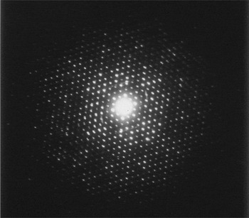
Figure 1: SAED pattern taken from a roughly 10-nm thick crystal of copper perchlorophthalocyanine. The diffraction spots extend to a resolution of better than 0.1 nm. The pattern was recorded on Lo Dose mammography film, from which a 2 × 2 slide was made. The slide was scanned to produce this figure, so the information in the original recording was of somewhat higher resolution than seen here. There are clear non-uniformities in the intensities that demonstrate that there is structural information in the pattern, and the intensities can be phased using direct methods to produce a map of the structure to atomic level.
An additional complication is that multiple scattering can be either coherent, called dynamical scattering, or incoherent, called secondary scattering. Dynamical scattering arises from a single, well-ordered crystal; whereas secondary scattering occurs when different parts of the crystal are characterized by different lattices, which can occur when different layers of a crystal are displaced from one another due to fractures, for example. In the latter case, a phase difference can arise due to different displacements at different positions, so secondary scattering depends on intensities, whereas dynamical scattering is in phase and depends on the amplitudes. In other words, in secondary scattering, the two or more scatterings are independent, whereas in dynamical scattering the second scattering is from states with well-defined phases. (In this paragraph I am using the term “phase” to mean the difference between the crest of a wave and a reference location. I'll refer to this simply as a “phase.”)
Dynamical scattering is less for low atomic weight specimens, large unit cells, thin crystals, and smaller scattering cross sections, which occur for higher voltages up to about 1 MV, and secondary scattering is less for well-ordered crystals. If the effects of multiple scattering can be made sufficiently small, neglecting them in the initial analysis, then recalculating taking multiple scattering into account, can lead to a successful determination of structure.
Background Subtraction
What one does next depends on the information that one is trying to obtain. In some cases just determining the lattice constants and symmetry will be sufficient, for example, to identify material phases. In other cases it will be necessary to measure the diffracted intensities accurately and determine the phases in order to reconstruct the potential and determine the atomic structure. In the former case it may only be necessary to least-squares fit the lattice and note any systematic absences of intensity, but in the latter case background intensity must be subtracted in order to obtain accurate values for the intensities. This is typically best done in two steps. Because the intensity of inelastic scattering, thermal diffuse scattering, and that from amorphous areas is usually large and non-linear, it is subtracted first, then a bilinear background subtraction eliminates the remaining background, including any inaccuracies from the first background subtraction.
The procedure for subtraction of the non-linear back-ground can be attributed to R.D.B. Fraser [Reference Fraser, Macrae, Suzuki and Tulloch1] and was modified by me [Reference Tivol, Chang and Parsons2]. For a single-crystal pattern, boxes are drawn around each lattice point. These must be big enough to include the diffraction spot, but no larger than necessary. The pixels within each box are then set to the average of the pixels on its edges. A rotational average is calculated with the center of rotation on the center of the pattern. When this rotational average is subtracted, almost all of the non-linear background is accounted for. Boxes are now drawn around each lattice point in the subtracted pattern. The intensity within each box is integrated, and the average intensity of the edges of each box is subtracted to account for the remaining background. See Figures 2 and 3 reproduced from [Reference Tivol, Chang and Parsons2].
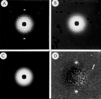
Figure 2: Subtraction of radially averaged background. A) Central part of SAED pattern from rat hemoglobin. B) Pattern after diffraction spots were replaced by the average of the local background. C) Radial average of the spot-subtracted pattern. D) Pattern from A after subtraction of C. Arrow points to the spot shown in Figure 3. The pattern was recorded on Lo Dose mammography film, which was scanned on a Perkin-Elmer microdensitometer to produce digital files from which a 2 × 2 slide was made. The slide was scanned, and ImageJ was used to remove dust and faded areas from the slide to produce this figure. The original of this figure was published in W.F. Tivol et al. (Reference Tivol, Chang and Parsons1982) and reproduced with permission. In the more than 25 years since this figure was produced, film has been replaced almost entirely by electronic acquisition with CCDs.
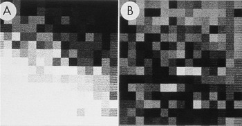
Figure 3: Enlarged area of the diffraction pattern in Figure 2. A) Before background subtraction, the spot indicated by the arrow in Figure 2 is hidden in the background. B) After background subtraction, the spot is clear. The intensity was calculated by performing a bilinear background subtraction on the box illustrated in B by fitting a plane to the intensities on the edge of the 15 × 15 pixel box surrounding the spot. The pixel values in the boxes both before and after subtraction were used to construct larger files with each value inserted into 10 rows and columns. The Perkin-Elmer microdensitometer was used in film-write mode to produce photographs from which a 2 × 2 slide was made. The slide was scanned, and ImageJ was used to remove dust and faded areas from the slide to produce this figure. The original of this figure was published in W.F. Tivol et al. (Reference Tivol, Chang and Parsons1982) and reproduced with permission.
Ring Patterns and Spot Patterns
Polycrystalline and ring patterns need to be treated differently. The radial averaging procedure does not work because there is no part of the pattern, or not enough, from which one can take an average background. In some cases the background can be modeled—for example, in a study of radiation damage—where the changes in the intensities of the coherent parts of the pattern were measured to determine how rapidly they decreased with radiation dose. The final pattern, which consisted only of scattering from disordered material, could be subtracted from the other patterns leaving only the contributions from ordered material. The final pattern had to be scaled to account for mass loss, and there was an apparent change in the nearest-atom distance as the material was irradiated, so the pattern had to be shifted as well. This model could be seen to work quite well for some data sets, but it was not as successful for others.
In the identification of material phases from single crystal spot patterns—or if there are only a few crystals, and spots can be assigned to particular crystals and indexed correctly—lattice constants can be determined by performing a least-squares fit, and systematic absences can often be determined just by looking at the pattern. (However, dynamical scattering can cause intensities to appear in the positions of systematic absences.) For ring patterns, the radius can be determined by least-squares fitting, and the presence or absence of rings at particular radii will indicate the symmetry. Gold is cubic so that the indices, h, k, and l, can only be either all odd or all even. Because the lattice vectors are of equal length, ring radii are equal to a constant times (h 2+ k 2+ l 2)1/2, so they are in ratios of 31/2:41/2:81/2:111/2:121/2…corresponding to (h k l) = (111), (002), (022), (113), (222), etc.
If one is trying to distinguish two material phases whose lattice constants are nearly the same, or if one needs to determine lattice vectors precisely, gold or another substance whose lattice constants are well-known can be evaporated onto a specimen, and measurement of both the diffraction from the specimen and radii of the gold rings will determine the lattice vectors and camera length accurately (see Figure 4). The procedure of evaporating a known substance onto a specimen eliminates inaccuracies in measurement caused by slight differences in specimen height, lens parameters, or other conditions that could occur if the specimen and the known substance were examined separately.
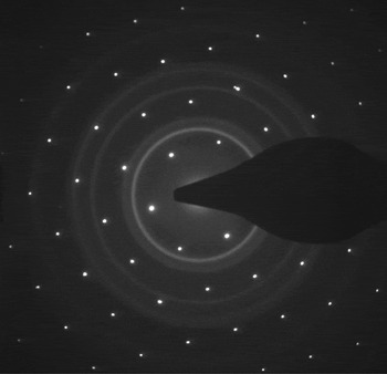
Figure 4: SAED pattern taken from a crystal of silicon onto which a thin layer of gold was vacuum evaporated. This pattern was taken by Carol Garland, a member of the professional staff and TEM facility manager for the Kavli Nanoscience Institute at Caltech.
Structure Determination
Structure determination from electron diffraction requires not only that the diffraction intensities be measured accurately, but that the correct phases be determined as well. These are really two aspects of the same thing because direct phasing methods give best results when the intensities are accurate. All the direct methods for determining phases can be derived from the unitary equation [Reference Tivol3], and because unitarity is a property of all known scattering processes, finding the correct phases is always possible if the intensities have been measured accurately enough. Furthermore, collection of images in addition to diffraction patterns gives those phases that are at resolutions out to the highest resolution in the image, so extension to the resolution of the diffraction pattern by direct methods is simplified.
The phases that are found, however, are for the diffraction amplitudes that include multiple scattering, and dynamical and/or secondary scattering effects must be removed to convert the diffraction data into structural information. If all the electrons are scattered at most once, the scattering is said to be kinematical, and if very few electrons are scattered two or more times, the scattering is called quasi-kinematical. In the former case once the phases have been determined, the structure can be computed by inverse Fourier transformation of the diffraction data. In the latter case, an initial structural determination will be close enough that further refinement will lead to the true structure.
D.L. Dorset et al. [Reference Dorset, Tivol and Turner4] analyzed diffraction data obtained on a high-voltage EM from copper perchlorophthalocyanine. The use of the highest available accelerating voltage, 1200 kV, and the preponderance of low atomic number atoms in the specimen allowed the data to be treated kinematically with no multiple scattering corrections. A subsequent analysis of similar data from copper perbromophthalocyanine [Reference Dorset, Tivol and Turner5] illustrates the quasi-kinematical case. The diffraction data were also obtained at 1200 kV, but the presence of the higher atomic number atoms of bromine led to sufficient dynamical scattering to give an initial structure that was not correct. Subsequent refinement was carried out by matching the experimental data to multi-slice calculations, which account for dynamical effects, and the final structure was accurately calculated. There was difficulty in producing an initial structure, however, and this led to the conclusion that copper perbromophthalocyanine is near the limit for successful application of ab initio direct phasing.
Because the amount of dynamical scattering depends on both crystal thickness and accelerating voltage, diffraction data from copper perchlorophthalocyanine crystals about 10 nm thick were examined at voltages ranging from 200 to 1200 kV (see Figure 5, reproduced from [Reference Tivol, Dorset, McCourt and Turner6]). Contrary to earlier calculations [Reference Jap and Glaeser7], which indicated an optimum voltage at about 500 kV, it was found that higher accelerating voltage gave better results.
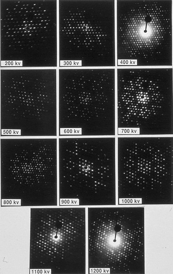
Figure 5: SAED patterns from crystals of copper perchlorophthalocyanine taken at various voltages on the HVEM at Albany, NY. Some of the crystals were very well ordered and very well aligned, for example, 700 kV and 1000 kV. Others are less well aligned, for example, 300 kV and 500 kV. Curvature of the Ewald sphere limits the resolution below 400 kV, particularly at 200 kV. The central “snowflake” in the 200 kV pattern is evidence of significant dynamical scattering. The patterns were recorded on Lo Dose mammography film from which a 2 × 2 slide was made. The slide was scanned and then cropped with ImageJ to produce this figure, so the information in the original recording was of somewhat higher resolution than seen here. The original of this figure was published in W.F. Tivol et al. (Reference Tivol, Dorset, McCourt and Turner1993) and reproduced with permission.
One possibility for success at lower voltages is to use extremely thin crystals. The crystals in Dorset et al. [Reference Dorset, Tivol and Turner4–Reference Dorset, Tivol and Turner5] were ~10 nm—or some 30-unit cells—thick, so preparing thinner crystals could be a challenge. One important example of this possibility is bacteriorhodopsin, which occurs naturally as a 2-D crystalline array in the plasma membrane of the bacterium Halobacterium halobium. N. Unwin, R. Henderson, and co-workers, in a series of papers beginning in 1975, produced structures at successively higher resolutions using diffraction data for the intensities and images for the phases [Reference Unwin and Henderson8, Reference Henderson and Unwin9, Reference Henderson, Baldwin, Downing, Lepault and Zemlin10, Reference Henderson, Baldwin, Cesca, Zemlin, Beckman and Downing11, Reference Subramaniam and Henderson12]. The last of these references reports a study for which a transient change, occurring upon illumination, was analyzed. X-ray crystallography has not been able to provide these data because the 3D crystals either did not allow the change or were altered and failed to diffract upon illumination, which makes this an example of a unique contribution of electron crystallography [Reference Henderson13].
Conclusion
Although there can be technical challenges in data interpretation for complete structure determination of unknown specimens, selected area electron diffraction is a powerful tool. In the case where the specimen consists of a few possible material phases, and the structures at particular areas need only to be identified as one of these phases, selected-area electron diffraction is a quick and simple method, requiring only that the area of interest be positioned within the area selected by the aperture and a diffraction pattern recorded.
Acknowledgments
This contribution was made from the Gordon and Betty Moore Center for Physical Biology while the author was employed there as a Senior Scientist. Partial support was also made by a grant from the National Institutes of Health (PI, Ahmed H. Zewail). This work benefited from use of the Caltech Kavli Nanoscience Institute and the Material Science TEM facilities partially supported by the MRSEC Program of the National Science Foundation under Award Number DMR-0520565.


