


Introduction
The conversion efficiency of Cu(In,Ga)(S,Se)2 (CIGSSe)-based solar cells is the highest of all thin film technologies with a record of 22.9% (Solar Frontier, 2017). One promising method of improving the efficiency is via creating a graded band gap in the absorber to suppress recombination effects at the interfaces (Gabor et al., Reference Gabor, Tuttle, Bode, Franz, Tennant, Contreras, Noufi, Jensen and Hermann1996). This is commonly achieved by a Ga/In or Se/S composition gradient towards the contacts. Surface-sulfurization has been demonstrated to be efficient in mitigating recombination at the buffer/absorber interface. It is anticipated that the sulfur incorporation leads to a down-shift of the valence band maximum (and an increase in conduction band minimum), resulting in an electronic barrier for majority charge carriers (holes) towards this interface (Singh et al., Reference Singh, Shafarman and Birkmire2006). The sulfurization is also argued to induce passivation of deep defect states (Kobayashi et al., Reference Kobayashi, Yamaguchi, Jehl Li Kao, Sugimoto, Kato, Hakuma and Nadaka2015).
Inconsistent results are found in the literature for the change in the device performance of sulfurized Cu(In,Ga)Se2 (CIGSe) solar cells. Improvements in the device performance after sulfurization treatment are mainly reported (Nakada et al., Reference Nakada, Ohbo, Watanabe, Nakazawa, Matsui and Kunioka1997; Ohashi et al., Reference Ohashi, Nakada and Kunioka2001; Probst et al., Reference Probst, Stetter, Riedl, Vogt, Wendl, Calwer, Zweigart, Ufert, Freienstein, Cerva and Karg2001; Kobayashi et al., Reference Kobayashi, Yamaguchi, Jehl Li Kao, Sugimoto, Kato, Hakuma and Nadaka2015; Kamanda et al., Reference Kamanda, Yagioka, Adachi, Handa, Fai Tai, Kato and Sugimoto2016; Huang et al., Reference Huang, Sung, Chen, Hsiao and Hsu2018; Kim et al., Reference Kim, Nishinaga, Kamikawa, Ishizuka, Nagai, Koida, Tampo, Shibata, Matsubara and Niki2018), whereas a few authors disclose a degraded performance (Singh, Reference Singh2009; Larsen et al., Reference Larsen, Keller, Lundberg, Jarmar, Riekehr, Scragg and Platzer-Björkman2018). The different results are understood to stem from variations in the modification of the material properties at the top region of the absorber, such as the occurrence of mixed phases, different sulfur concentrations and microstructural changes induced by the sulfurization treatment. It has been shown that a certain amount of sulfur is necessary to increase the open-circuit voltage (V OC) (Nagoya et al., Reference Nagoya, Kushiya, Tachiyuki and Yamase2001; Alberts, Reference Alberts2009), above which the fill factor (FF) starts to drop. The degradation of the device performance is suggested to be related with the formation of a barrier for the current collection through the growth of a fully converted sulfide layer (Singh et al., Reference Singh, Shafarman and Birkmire2006). The sulfur incorporation is dependent on the composition (specifically the Cu and Ga concentrations) as well as the mean grain size in the absorber layer, which can vary according to the fabrication technique and parameters implemented (Titus et al., Reference Titus, Schock, Birkmire, Shafarman and Singh2001). CIGSSe can be synthesized by the reaction of metal precursors deposited at elevated temperatures followed by a selenization + sulfurization treatment (Nagoya et al., Reference Nagoya, Kushiya, Tachiyuki and Yamase2001), or by co-evaporation/co-sputtering using physical vapor deposition techniques (Kobayashi et al., Reference Kobayashi, Yamaguchi, Jehl Li Kao, Sugimoto, Kato, Hakuma and Nadaka2015). The sulfur inclusion is also dependent on the method and conditions of the sulfurization treatment. Sulfurization can be carried out in several ways, either by annealing of the absorbers in H2S atmosphere (Kamanda et al., Reference Kamanda, Yagioka, Adachi, Handa, Fai Tai, Kato and Sugimoto2016), evaporation of In2S3 onto the absorber surface and annealing in sulfur vapor (Ohashi et al., Reference Ohashi, Nakada and Kunioka2001), or using elemental evaporation of sulfur (Mueller et al., Reference Mueller, Mock, Haug, Hergert, Koehler, Zweigart and Herr2015), respectively. Generally, a smooth Se/S gradient is desirable at the top region of the absorber, where sulfur atoms replace selenium atoms while maintaining the chalcopyrite compound structure. Avoiding the formation of a separate phase on top is understood to produce higher conversion efficiency performances (Ohashi et al., Reference Ohashi, Nakada and Kunioka2001). However, contingent to the absorber composition and sulfur treatment, separate phases have been reported to form due to the diffusion of sulfur, where the CuInS2 phase is most commonly detected at the surface of the absorber (Singh et al., Reference Singh, Shafarman and Birkmire2006). Sulfurized CIGSe absorbers with a fully converted sulfide phase formed on top also show contradictory device performance results (Singh, Reference Singh2009; Kobayashi et al., Reference Kobayashi, Yamaguchi, Jehl Li Kao, Sugimoto, Kato, Hakuma and Nadaka2015). Hence, high-resolution analyses are necessary to determine the local composition of such regions in more detail. The distribution of sulfur in the grain interiors (GIs) and at grain boundaries (GBs) after sulfurization treatments is a matter that requires further study. In a previous investigation performed on CIGSe solar cells (Larsen et al., Reference Larsen, Keller, Lundberg, Jarmar, Riekehr, Scragg and Platzer-Björkman2018), using energy dispersive X-ray spectroscopy (EDS) in scanning transmission electron microscopy (STEM) we have demonstrated that a CuInS2 phase forms at the surface after sulfurization along with a ~10 nm thick Ga-rich interphase (presumably CuGaS2) underneath. In this work, we investigate the issue in further detail by performing atom probe tomography (APT) for one of the sulfurized CIGSe absorbers examined in Larsen et al. (Reference Larsen, Keller, Lundberg, Jarmar, Riekehr, Scragg and Platzer-Björkman2018), where APT provides here an atomic level quantification of the sulfur distribution in three dimensions. Local composition analysis is performed at the top region of the CIGSe absorbers as well as at lattice defects.
Materials and Methods
CIGSe absorbers were co-evaporated on Mo-coated soda lime glass substrate at Solibro Research AB and post-sulfurized in a custom-built furnace using elemental sulfur (avoiding the use of toxic H2S gas) at a controlled preheated set temperature of 500°C and 50 mbar Argon pressure for 20 min. More details on the synthesis part are provided in Larsen et al. (Reference Larsen, Keller, Lundberg, Jarmar, Riekehr, Scragg and Platzer-Björkman2018). STEM imaging was conducted at 200 kV acceleration voltage in a FEI Titan Themis TEM system using a SuperX system for EDS analysis.
A dual-beam focused ion-beam/scanning electron microscopy (FIB/SEM) workstation (FEI Versa 3D) was used to perform site-specific sample preparations for APT analysis via the standard lift-out technique (Thompson et al., Reference Thompson, Lawrence, Larson, Olson, Kelly and Gorman2007). Chromium was deposited on top as a capping layer, with ~200 nm thickness, using magnetron sputtering to protect the region of interest. A 100 nm thick Pt layer was deposited on top of the Cr layer using the electron beam in the FIB/SEM to minimize Ga implantation. A voltage of 2 kV was used during the final shaping of the APT tip specimens. APT measurements were performed in a LEAP™ 3000X HR CAMECA™ system in laser pulsing mode with a repetition rate of 100 kHz, 0.05 nJ laser power and a base temperature of ~50 K. The data were reconstructed and analyzed using the software CAMECA™ IVAS 3.6.14. All concentration values are given in at%.
Results
Figure 1a shows a STEM dark-field image for a cross-section of the CIGSe absorber after the sulfurization treatment. A surface reaction layer is clearly observed at the top-region, which is further highlighted using high angle annular dark-field imaging (HAADF) shown in Figure 1b. The absorber surface appears to be relatively rough where the morphology is closely connected to the grain structures. EDS maps in Figure 1b displays the distribution of the elements in the absorber layer. An enrichment of Ga and a depletion of In is visible towards the back contact. This gradient is produced during deposition to attain a back-surface field for driving electrons away from the defect-rich back contact (Contreras et al., Reference Contreras, Tuttle, Gabor, Tennant, Ramanathan, Asher, Franz, Keane, Wang, Scofield and Noufi1994). Some enrichment of Ga, Cu, In, and S is observed at the upper region as well as depletion of Se. A STEM EDS line scan was performed for the top 350 nm of the absorber to elucidate the composition within this region, presented in Figure 1c. Two sulfur-rich layers can be observed. The upper one (~30 nm thick) shows Cu ~28%, In ~23%, S ~45%, Ga<5% and almost no Se. This composition fits to a CuInS2 phase, which was detected by gracing incidence X-ray diffraction in our previous work (Larsen et al., Reference Larsen, Keller, Lundberg, Jarmar, Riekehr, Scragg and Platzer-Björkman2018). The lower layer (~10 nm thick) shows Cu ~26%, In ~13%, S ~23%, Ga ~14%, and Se ~23%, showing Ga enrichment and In depletion.
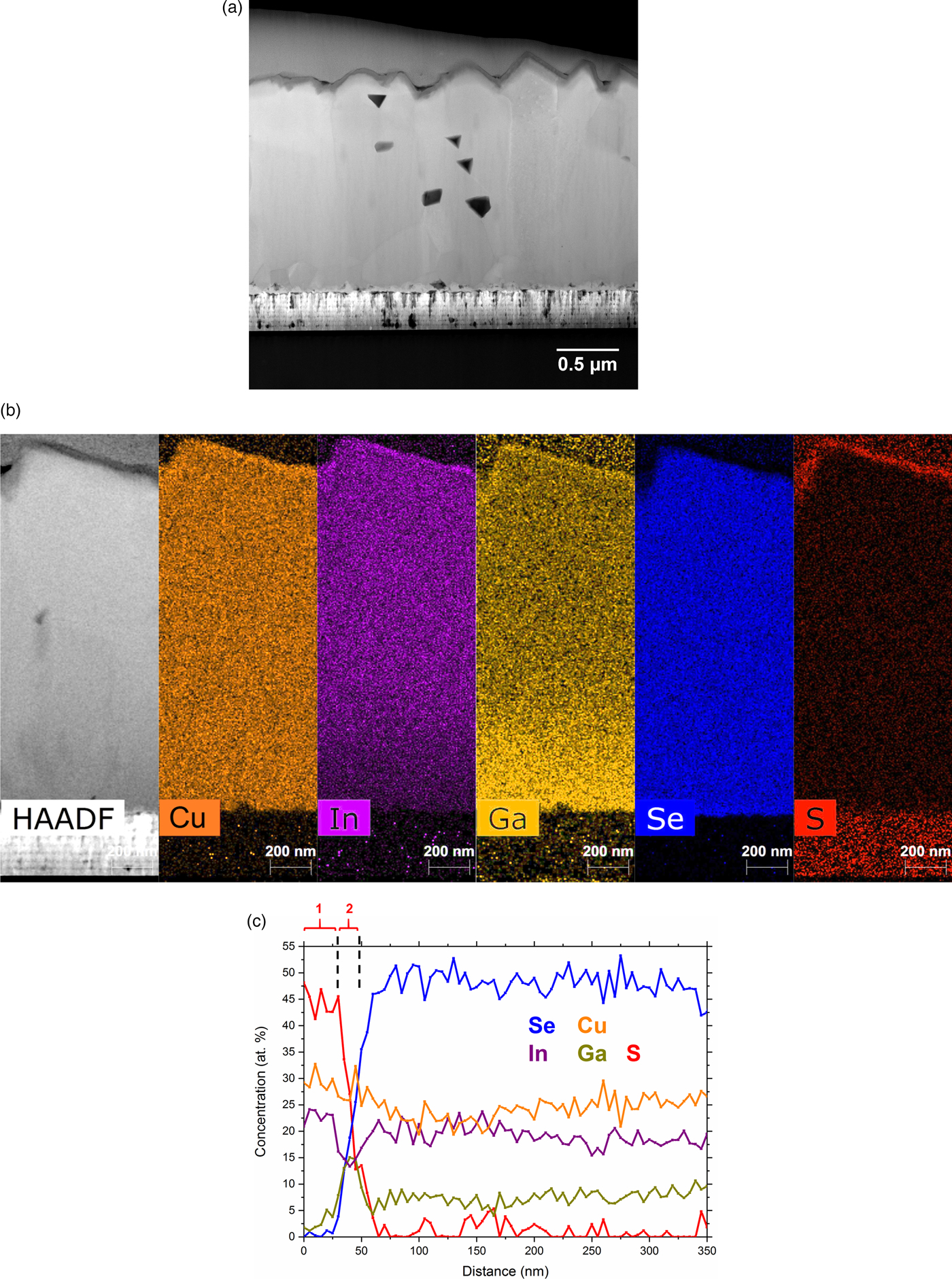
Fig. 1. a: STEM image for the sulfurized CIGSe sample. b: HAADF image and corresponding elemental STEM-EDS maps. c: STEM-EDS line-scan of the elemental composition near the surface region (the two sulfur-rich layers are marked by “1” and “2”).
Atom probe tips were prepared from the same sample, with their main axis perpendicular to the substrate surface. The tips were extracted from areas showing grooves along the surface which most likely exhibit a GB in the CIGSe underneath. Figure 2a displays an APT reconstruction from the sulfurized absorber, with the sulfur-rich region on top, as well as a GB in the absorber. Strong segregation of sodium is detected at the GB in which Na atoms diffused from the soda lime glass substrate during film growth. However, some fine traces of sodium are also detected in the sulfur-rich region. Diffusion of foreign Na atoms to lattice defects is widely known for CIGSe systems (Cadel et al., Reference Cadel, Barreau, Kessler and Pareige2010; Schlesiger et al., Reference Schlesiger, Oberdorfer, Würz, Greiwe, Stender, Artmeier, Pelka, Spaleck and Schmitz2010; Choi et al., Reference Choi, Cojocaru-Mirédin, Wuerz and Raabe2011; Cojocaru-Mirédin et al., Reference Cojocaru-Mirédin, Choi, Abou-Ras, Schmidt, Caballero and Raabe2011a, Reference Cojocaru-Mirédin, Choi, Wuerz and Raabe2011b; Abou-Ras et al., Reference Abou-Ras, Schmidt, Caballero, Unold, Schock, Koch, Schaffer, Schaffer, Choi and Cojocaru-Mirédin2012) in that it commonly displays positive effects on the device performance, such as increased p-type conductivity and higher V OC (Singh & Patra, Reference Singh and Patra2010). Interestingly, segregation of S atoms is also detected at the GB here, presenting a broader distribution across the boundary compared with Na. Figure 2b shows 1-D concentration profile across the GB highlighting the segregation of Na and S atoms. Gibbs interfacial excess is measured here to evaluate the segregations at the GB. It offers a more precise quantification compared with 1-D concentration profiles since it is less affected by ion-trajectory aberrations and interface morphology effects (Hellman & Seidman, Reference Hellman and Seidman2002). The Gibbs interfacial excess of Na measured along the GB plane is ΓNa = 1.2 (±0.3) at./nm2, which fits well within ΓNa values for random high angle GBs of CIGSe reported in Cojocaru-Mirédin et al. (Reference Cojocaru-Mirédin, Schwarz and Abou-Ras2018). Figure 2c shows the Gibbs interfacial excess of sulfur measured from top to bottom along the GB plane at different depths. The decay of ΓS denotes the diffusion of sulfur atoms from top to bottom. Segregations of sulfur reach up to ~7 at% at the uppermost part of the GB. Minor composition fluctuations are observed for other elements at the vicinity of the boundary (see Fig. 2b), which is often reported using APT analysis on CIGSe, such as in Keller et al. (Reference Keller, Schlesiger, Riedel, Parisi, Schmitz, Avellan and Dalibor2013; and Stokes et al. (Reference Stokes, Al-Jassim, Diercks, Clarke and Gorman2017). The composition and segregations measured at the GB region in CIGSe compounds are argued to diverge depending on the nature of the GB and the corresponding grain orientations.
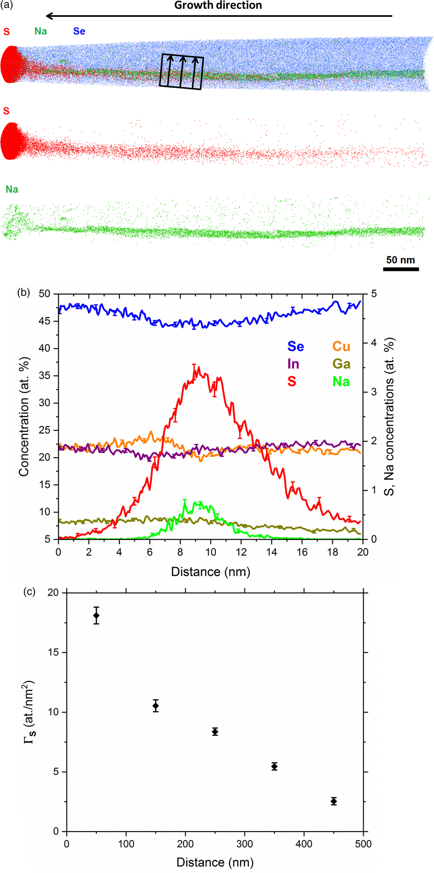
Fig. 2. a: APT reconstruction for the sulfurized CIGSe sample showing the sulfur-rich region at the top of the absorber and a GB in the absorber displaying segregation of Na and S atoms. b: 1-D concentration profile across the GB (region highlighted in the reconstruction). c: Gibbs interfacial excess (Γ) for sulfur as a function of distance along the GB (from top to bottom direction).
A local mass spectrum from the region of the GB is presented in Figure 3. The spectrum contains 1.5 million atoms with a background noise level of ~35 ppm, and mass resolving power of ~1,200 full width at half maximum (calculated on 115In+1 peak). Single and complex ions are detected, respectively, marked in Figure 3. An overlap for some Se+1 and Se2+2 peaks exists in the spectrum, which is deconvoluted using the natural isotope abundance ratios. If sufficient oxygen exists in the sample, another overlap would be expected for O+1 and S+2 at 16 Da as well as for O2+1 and S+1 at 32 Da. Such overlaps would be difficult to deconvolute in the spatial reconstruction. Oxygen as an impurity can diffuse along CIGSe GBs during the layer deposition or from the substrate, which was reported by some authors, such as in Oana Cojocaru-Mirédin et al. (Reference Cojocaru-Mirédin, Choi, Abou-Ras, Schmidt, Caballero and Raabe2011a, Reference Cojocaru-Mirédin, Choi, Wuerz and Raabe2011b) and Abou-Ras et al. (Reference Abou-Ras, Schmidt, Caballero, Unold, Schock, Koch, Schaffer, Schaffer, Choi and Cojocaru-Mirédin2012). Regarding sulfur detection, only one main peak at 32 Da is detected in the spectrum here, while no peak at 16 Da is observed. Furthermore, a small peak is detected at 34 Da that belongs to the second isotope of sulfur (34S+1). A very good fit is found when comparing the 34S+1/32S+1 ratio detected experimentally to the natural isotope abundance ratios. Several other tips from the same sample have shown similar results. Nevertheless, we cannot exclude the possibility of having traces of oxygen at the GBs that we have analyzed, which could be below the detection limit here. However, it is important to note that the diffusion of oxygen along CIGSe GBs can be highly dependent on the deposition technique and conditions. It is also essential to note that some slight traces of potassium (~0.01 at%) were detected at the GB region which also originates by diffusion from the soda lime substrate.

Fig. 3. Local mass spectrum from the GB region. The inset (top-right) displays a spectrum range between 15 and 42 Da for better visualization of the Na, S, and K peaks.
A 1-D composition profile through the uppermost 100 nm of the APT reconstruction shown in Figure 2 is plotted in Figure 4. The volume for the plotted profile is within a region slightly distant from the GB segregations. The profile shows a close agreement with the STEM-EDS line scan displayed in Figure 1c. Two sulfur-rich layers can be identified, where ~10 nm thick Ga-rich layer exists underneath the uppermost Se and Ga depleted layer. In the uppermost layer, the sulfur composition is almost at 50 at% and Ga is below 2 at%. The Cu and In concentrations within this uppermost layer are slightly different as compared with the EDS line scan. Such differences in the composition can arise due to the effect of the lamella thickness and beam interaction volume compared with the localized APT analysis. Furthermore, the compositions may slightly vary in different grains within the CuInS2 phase (Keränen et al., Reference Keränen, Lu, Barnard, Sterner, Kessler, Stolt, Matthes and Olsson2001). It is important to mention that the sulfur concentration drops down below 1 at% underneath the Ga-rich interlayer, which reflects that the absorber grains here are not much influenced by the sulfurization process, rather the incorporated sulfur is highly concentrated at the surface and in the GBs in the absorber.

Fig. 4. 1-D concentration profile along the uppermost 100 nm of the APT reconstruction displayed in Figure 2.
Discussion
The experimental results herein reveal further insights on the sulfur distribution within sulfurized CIGSe resulting from the applied sulfurization process (Larsen et al., Reference Larsen, Keller, Lundberg, Jarmar, Riekehr, Scragg and Platzer-Björkman2018). The formation of a separate sulfur-rich area at the top-region of the absorber is observed using both STEM-EDS and APT techniques. Since the CIGSe absorber is fully selenized and crystallized before the sulfurization treatment, it is expected that a new sulfur containing layer is formed at the surface instead of a direct in-diffusion of sulfur into the CIGSe lattice. The absorber is deposited with a Cu-poor composition (Cu/III ratio ~0.82) in order to suppress the formation of secondary copper chalcogenides, which means that the lattice contains high concentrations of Cu-vacancies. The adsorption of sulfur at the surface is suggested to create a driving force for cations (Cu and In) to diffuse via the VCu point defects towards the surface and bond with sulfur atoms. According to quaternary phase diagram calculations of the Cu-In-Ga-Se and Cu-In-Ga-S systems (Stephan, Reference Stephan2011), the Cu(In,Ga)S2 phase exhibits a narrower solubility range compared with Cu(In,Ga)Se2. Hence, off-stochiometric compositions of a Cu-In-Ga-S solid solution would easily promote a decomposition into In-rich and Ga-rich solid solutions under equilibrium conditions. The CuInS2 phase is expected to nucleate and grow from the In-rich Cu-In-Ga-S solid solution. CuInS2 will grow further as more sulfur atoms are adsorbed on the surface along with Cu and In atoms diffusing outwards from the absorber lattice driven by the high copper-vacancy concentration. Therefore, the Ga-rich interlayer is understood to form here as a result of a decomposition process during the early stages of sulfurization. Phase separation was frequently reported for Cu-In-Ga-Se systems at relatively low deposition temperatures (typically 300–400°C), such as in Keränen et al. (Reference Keränen, Lu, Barnard, Sterner, Kessler, Stolt, Matthes and Olsson2001) and Moon et al. (Reference Moon, Yun, Gwak, Ahn, Cho, Shin, Yoon and Ahn2012). The Gibbs free energy of mixing for Cu-In-Ga-Se solid solution (at 87°C), calculated in Xue et al. (Reference Xue, Lu, Tang, Li, Zhang and Feng2014), exhibits three minima points and two unstable regions (spinodal decompositions). The three minima points correspond to In-rich CIGSe, Cu(In,Ga)Se2, and Ga-rich CIGSe compositions. Thus, based on such calculations, the Ga-rich Cu(In,Ga)(Se,S)2 interlayer with ~12 at% In is considered to be a metastable phase. No CuGa(SeS)2 phase was detected in the current sample using X-rays diffraction in our previous study (Larsen et al., Reference Larsen, Keller, Lundberg, Jarmar, Riekehr, Scragg and Platzer-Björkman2018).
In the literature, different compositions and sulfur-rich phases are reported to form at the CIGSe surface after the sulfurization treatment, where in most cases improvements in the device performance are measured. Huang et al., have reported a drop in In, Cu, Se, and Ga concentrations at the top 60 nm using secondary ion mass spectrometry where a Cu(In,Ga)(SeS)2 phase was detected after the sulfurization treatment resulting in ~1.9% increase in efficiency (Huang et al., Reference Huang, Sung, Chen, Hsiao and Hsu2018). Kobayashi et al., have observed a drop in In and a rise in Ga concentrations in the top 100 nm using X-ray photoelectron spectroscopy after sulfurization, where the solar cell device showed 2.2% efficiency enhancement (Kobayashi et al., Reference Kobayashi, Yamaguchi, Jehl Li Kao, Sugimoto, Kato, Hakuma and Nadaka2015). Several processing factors, such as sulfur gas pressure or deposition temperature, can contribute to the compositional changes and phase formations during the sulfurization treatment resulting in such variations. The corresponding solar cell devices, processed from the absorber presented in this study have shown degraded FF values and conversion efficiency values of up to ~6% lower compared with non-sulfurized samples (Larsen et al., Reference Larsen, Keller, Lundberg, Jarmar, Riekehr, Scragg and Platzer-Björkman2018). One may argue that the formation of a separate CuInS2 phase is causing such an undesirable performance. Comparison of relative device improvements should also be done with caution since low performing devices can be improved more easily. Nonetheless, in other works such as in Kim et al. (Reference Kim, Nishinaga, Kamikawa, Ishizuka, Nagai, Koida, Tampo, Shibata, Matsubara and Niki2018), CIGSe solar cells were sulfurized and similarly display CuInS2 phase formation at the absorber surface, while on the contrary, improvements in the device performance were recorded. Based on the STEM-EDS and APT results here, the device performance improvement is likely to depend on whether single or multiple sulfide phases form in the sub-surface region. Multiple sulfide phases exhibit dissimilar diode properties, which creates an electron transport barrier correspondingly. Simulations of the band diagram of the sulfurized sample analyzed here have shown a conduction band offset (CBO) of 0.54 eV between the Ga-rich CuInGa(Se1−zSz)2 interlayer and the CIGSe absorber, and an offset of 0.18 eV between the CuInS2 phase and Ga-rich CuInGa(Se1−zSz)2 interlayer (Larsen et al., Reference Larsen, Keller, Lundberg, Jarmar, Riekehr, Scragg and Platzer-Björkman2018). In particular, the first-mentioned CBO is supposed to act as an effective electronic barrier. Furthermore, both (newly created) interfaces exhibit additional, potential areas of high recombination velocities. Hence, phase separation should, therefore, be mitigated within the sulfur-rich regions. One possible approach to avoid phase separation is by having Ga-poor compositions at the top part of the absorber. Indeed, in the three-stage synthesis process of the CIGSe absorbers in the work of Kim et al. (Reference Kim, Nishinaga, Kamikawa, Ishizuka, Nagai, Koida, Tampo, Shibata, Matsubara and Niki2018) no Ga was deposited in the third stage (upper region of the absorber), which can be expected to have circumvented the formation of a Ga-rich interlayer.
The diffusion of sulfur in GBs of CIGSe has been discussed in the literature, due to the clear correlation between the sulfur incorporation and the grain sizes of the absorber layer, where higher sulfur content was detected in microstructures with finer grains (Nakada et al., Reference Nakada, Ohbo, Watanabe, Nakazawa, Matsui and Kunioka1997; Basol et al., Reference Basol, Halani, Leidholm, Norsworthy, Kapur, Swartzlander and Matson2000; Probst et al., Reference Probst, Stetter, Riedl, Vogt, Wendl, Calwer, Zweigart, Ufert, Freienstein, Cerva and Karg2001; Titus et al., Reference Titus, Schock, Birkmire, Shafarman and Singh2001). The broad spread of the sulfur profile observed here across the GB (see Fig. 2b) indicates some outward diffusion of sulfur into the GI. This is also supported by similar results, from APT analysis of sulfurized CIGS solar cells made from metallic precursor layers (Keller et al., Reference Keller, Schlesiger, Riedel, Parisi, Schmitz, Avellan and Dalibor2013), that show increased sulfur concentration in smaller grains due to the enhanced effective diffusivity. It is important to point out that the distribution of alkali metals does not appear to be affected by the sulfur diffusion into the GBs. This is an important advantage of using sulfur to tune the bandgap at the vicinity of the p-n junction since the segregation of alkali metals (e.g. Na, K, Rb or Cs) at GBs is understood to have beneficial effects on the device performance. However, it cannot be excluded that the sulfur in-diffusion forms Na-S-(O) compounds in the GBs, which might reduce a possible passivating effect and thereby reduce V OC. Furthermore, these Na-S-(O) phases might be conductive and locally shunt the p-n junction, resulting in bad diodes and eventually in a reduction in FF and V OC. Another possibility is a negative influence from Na-S-(O) phases on CdS growth as was shown for Cu2ZnSnS4 devices (Ren et al., Reference Ren, Scragg, Edoff, Larsen and Platzer-Björkman2016).
Conclusions
High-resolution microstructural analysis using STEM-EDS and APT techniques was conducted on a CIGSe absorber post-sulfurized by using an elemental sulfur source. The results highlight the re-distribution of matrix elements as a result of the sulfurization treatment at the upper region of the absorber, where two distinct sulfur-rich phases were formed. Sulfur atoms also segregate at the GBs of the absorber which declines with the distance from the surface. The presence of multiple sulfur-rich phases is anticipated to be causing an electron transport barrier leading to a reduction in the device performance after the sulfurization treatment. In the cases where the formation of a single sulfur-rich phase at the absorber surface is inevitable, the deposition of CIGSe absorbers with Ga-poor compositions near the surface is predicted to hinder the nucleation of a Ga-rich interlayer.
Acknowledgments
The authors would like to acknowledge the funding from the Swedish Foundation for Strategic Research (SSF) through the RMA15-0030 project. They also thank the colleagues in the solar cell group at the Ångström lab and at Solibro Research AB.


 Open access