


Introduction
A current trend in a surface investigation can be defined, both in academia and industry, as follows: (i) the need to characterize and analyze structures in the (sub)nanometer range is growing; (ii) the complexity of such measurements across various instruments creates a demand for advanced correlative analysis; and (iii) easy-to-use instrumentation and automated procedures are of great interest.
Atomic force microscopy (AFM) and scanning electron microscopy (SEM) are two of the most used techniques for sample nanoscale analysis. To tackle market demands, NenoVision has developed a unique AFM, the LiteScope™, designed for integration into the SEM. The motivation behind the design is twofold: first, such a hybrid system allows for efficient, yet complex in situ sample characterization, and, second, it brings new possibilities for advanced correlative imaging, which allows sample analysis in a way that was difficult or impossible by separate SEM and AFM systems.
In SEM, the sample surface is scanned with a focused primary electron beam [Reference Crouzier1]. This interaction produces various signals that, through a range of detectors, provide different information about the surface and its chemical composition [Reference Flegler2]. In combination with focused ion beam (FIB), SEM is also used for surface modification. In general, a 2D SEM image provides great material contrast and a large depth of focus [Reference Beauvais3], all in a wide range of imaging resolutions down to around 1 nm.
On the other hand, an AFM scans the sample surface with a sharp tip and measures attractive and repulsive forces emerging between the tip and the sample [Reference Jalili and Laxminarayana4]. Thanks to this principle, AFM can provide sub-nanometer resolution combined with information on topography, roughness, mechanical, and magnetic and electrical properties depending on the probe used. Thus, the integration of AFM inside a SEM combines the capabilities of both techniques and brings many advantages.
AFM-in-SEM integration enables true correlative imaging where the region of interest (ROI) on the sample is analyzed by AFM and SEM at the same time. Traditionally, the correlation is achieved by imaging the sample by a number of techniques, subsequently followed by data analysis and final image overlay, for example, correlative Raman imaging and scanning electron microscopy (RISE) is in this category [Reference Matheson5]. There are also approaches for simultaneous measurements of multiple signals such as correlative light-electron microscopy (CLEM) that combines an optical microscope with an SEM into one system [Reference DeBoer6]. Common issues with traditional approaches are either high initial investment into sophisticated, dedicated instruments or problematic image correlation due to data incompatibility (data formats, pixel count and size, etc.) between devices used [Reference Mitchell7]. LiteScope is equipped with Correlative Probe and Electron Microscopy (CPEM)™ technology that enables simultaneous data acquisition and correlation of multiple channels; for example, the material contrast given by SEM is merged with the 3D topography of surface features obtained by AFM, resulting in a 3D CPEM view (Figure 1).
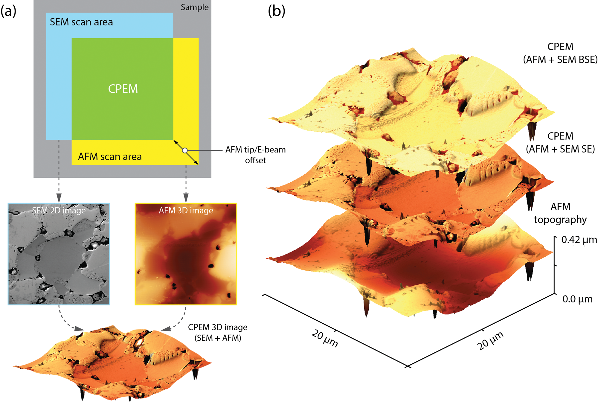
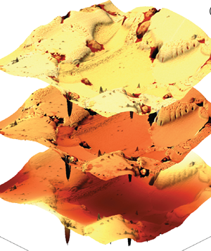
Figure 1: CPEM principle and CPEM view. (a) Schematics illustrate the sample area scanned simultaneously by AFM tip and SEM electron beam. Acquired data are correlated to create the resulting 3D CPEM view that can accommodate multiple signals (for example, AFM topography with SEM secondary and back-scattered electrons), as demonstrated by a tungsten-chromium sample containing hafnium oxide particles (b).
Another key advantage of the AFM-in-SEM approach is in situ measurement, meaning minimal sample handling and contamination due to vacuum preservation inside the SEM, which is crucial for sensitive samples. Also, using SEM, the AFM tip can be navigated with nanometer precision to the ROI, which makes obtaining measurements extremely time-efficient and eliminates the need for navigation marks made by FIB milling.
Lastly, the entire system is highly customizable (for example, scanner configuration, immersion lens compatibility) and can be equipped with many additional accessories, such as a nanoindenter or tweezers, that further broadens possibilities of the AFM-in-SEM concept for complex and efficient sample analysis.
This article demonstrates the abilities and advantages of CPEM technology in AFM-in-SEM applications as well as use of the LiteScope as a stand-alone AFM. Technical aspects of the system, including self-sensing probes and supported measurement modes, are detailed in the Methods section. The applications discussed cover a combination of key features and measurement modes including topography in combination with material, electrical, and mechanical properties and FIB milling applications.
Materials and Methods
LiteScope is a compact AFM microscope (129 × 90 × 45 mm), designed to fit into the SEM chambers of most microscope manufacturers (TESCAN, Zeiss, ThermoFisher Scientific, Hitachi, JEOL) and can be easily mounted on the SEM stage through a dedicated adaptor (Figure 2). It is a highly customizable plug-and-play solution with optional scanner configurations (both in open- and closed-loop mode) with a version compatible with magnetic immersion SEM, and installation takes only a few minutes. The standard configuration offers a large scanning area up to 100 × 100 × 100 µm and a resolution down to 0.2 nm. An optional scanner configuration improves resolution to 0.07 nm and decreases the scanning area to 38 × 38 × 38 µm. Further customization includes specimen exchange through the SEM load-lock system [Reference Kohl-Roscher8] or addition of a nanoindenter module or specialized sample and probe holders.
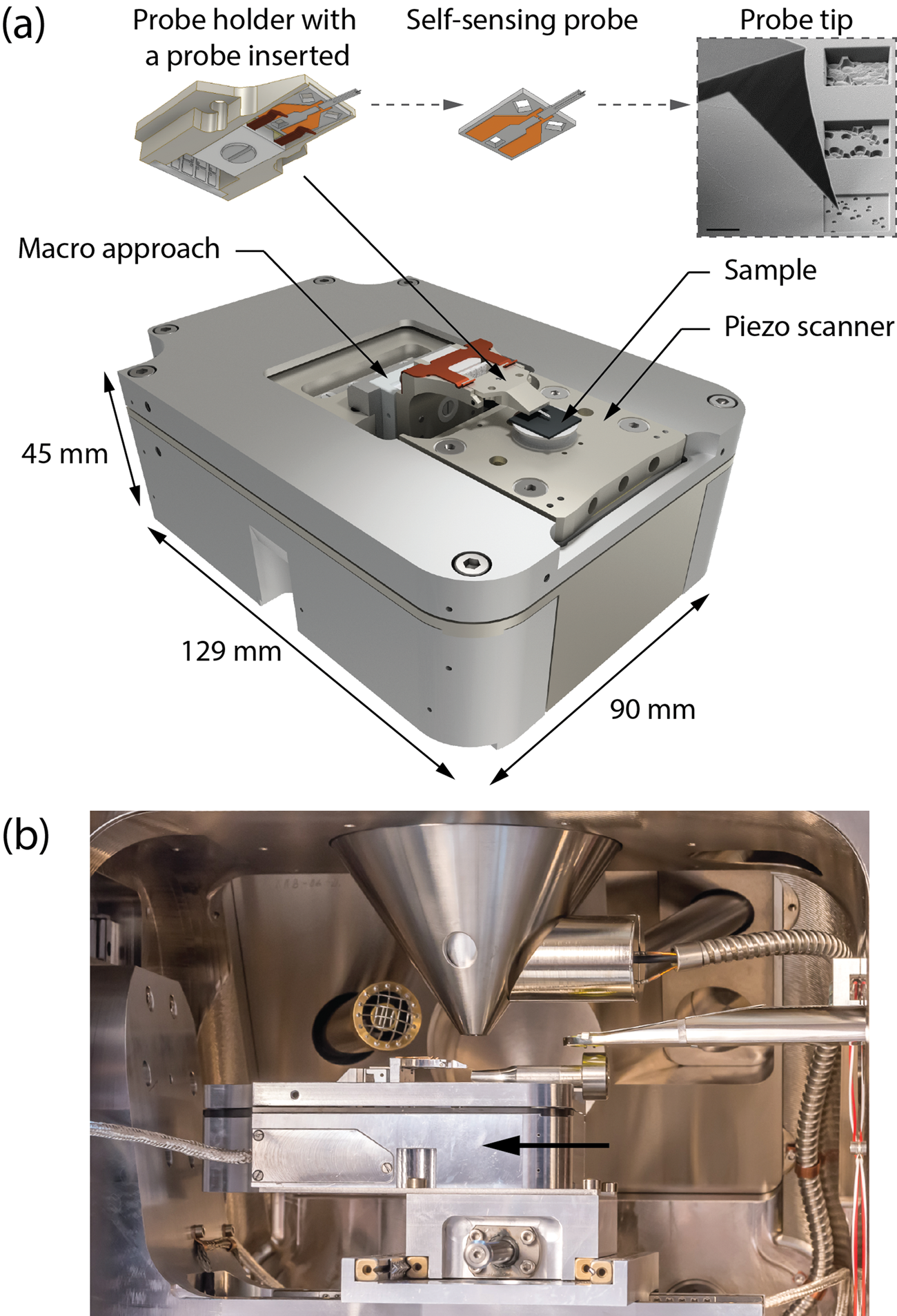
Figure 2: The AFM module can be easily integrated into existing SEMs. (a) Schematics showing the main dimensions and parts of the microscope, including the AFM probe. (b) The arrow highlights the scanhead mounted inside the SEM chamber.
The system includes the NenoBox™ control unit, which is connected to both the AFM and SEM detectors. This allows simultaneous acquisition and correlation of AFM and SEM signals through CPEM technology. Data are visualized and processed in NenoView™, a web-based software package that does not require pre-installation or a dedicated computer. Data can be accessed from any device connected to the internet or local network. CPEM technology allows for true data correlation, and some applications are detailed in the Results and Discussion section.
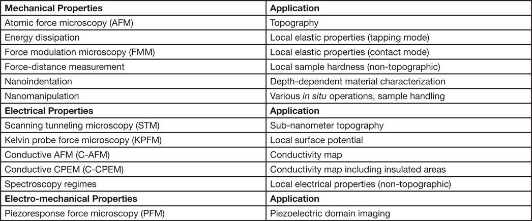
Compatibility with a variety of self-sensing and self-actuating probes operated up to 75 kHz, based on a tuning fork principle or piezoresistive cantilever, significantly extends capabilities of the instrument [Reference Wu9]. A list of supported techniques is presented in Table 1. Additionally, self-sensing probes eliminate several disadvantages of traditional AFM cantilevers with optical detection, such as the need for frequent laser alignment, imaging artifacts, and optical diffraction limitations [Reference Dukic10]. Use as a dedicated AFM with NenoCase™, which is designed to dampen vibrations and to allow measurements under different atmospheres, is also possible.
Table 1: List of measurement modes supported by the LiteScope.
Results and Discussion
Correlative microscopy
CPEM represents a unique approach to correlative imaging since it enables simultaneous acquisition of SEM and AFM data and precisely merges them. Thus, the differences between material (SEM) and topography (AFM) contrast can be quickly and precisely distinguished. The working principle of CPEM is as follows: the SEM view enables precise positioning of the AFM probe to the ROI on the sample mounted on the LiteScope's piezo scanner. Then, the electron beam is focused near the AFM tip, and the SEM is set to point or spectroscopy mode. The AFM tip, as well as the electron beam, remain stationary during data acquisition, and scanning is conducted solely by the piezo scanner. This configuration ensures a constant offset between the AFM and SEM images, which is removed in a postprocessing step [Reference Neuman11]. The result is a perfect correlation of multiple signals providing insight into the sample surface properties. The data can be also displayed in a scalable 3D view, which may help facilitate data interpretation (Figure 1a). CPEM can accommodate several types of signals including secondary (SE) and back-scattered electrons (BSE) (Figure 1b), electron beam induced current (EBIC), and cathodoluminescence (CL).
Figure 3 illustrates the use of CPEM on two samples, exfoliated WSe2 flakes on Si nanopillars and a duplex steel sample. Figure 3a shows a multilayered WSe2 flake, which is deformed by placement on 100 nm high Si nanopillars. A monolayer of WSe2 is barely visible in the SEM image, but it is clearly visible by AFM topography. Localization of such a small structure by separate AFM and SEM instruments would be an extremely tedious process with a high level of uncertainty, which is eliminated by the AFM-in-SEM approach. The scalable 3D CPEM view of correlated data helps to visualize and understand how the flakes cover the nanopillars. A certain shape of the WSe2 monolayer over the nanopillars creates a single-photon emitter useful for quantum cryptography for secure communications.
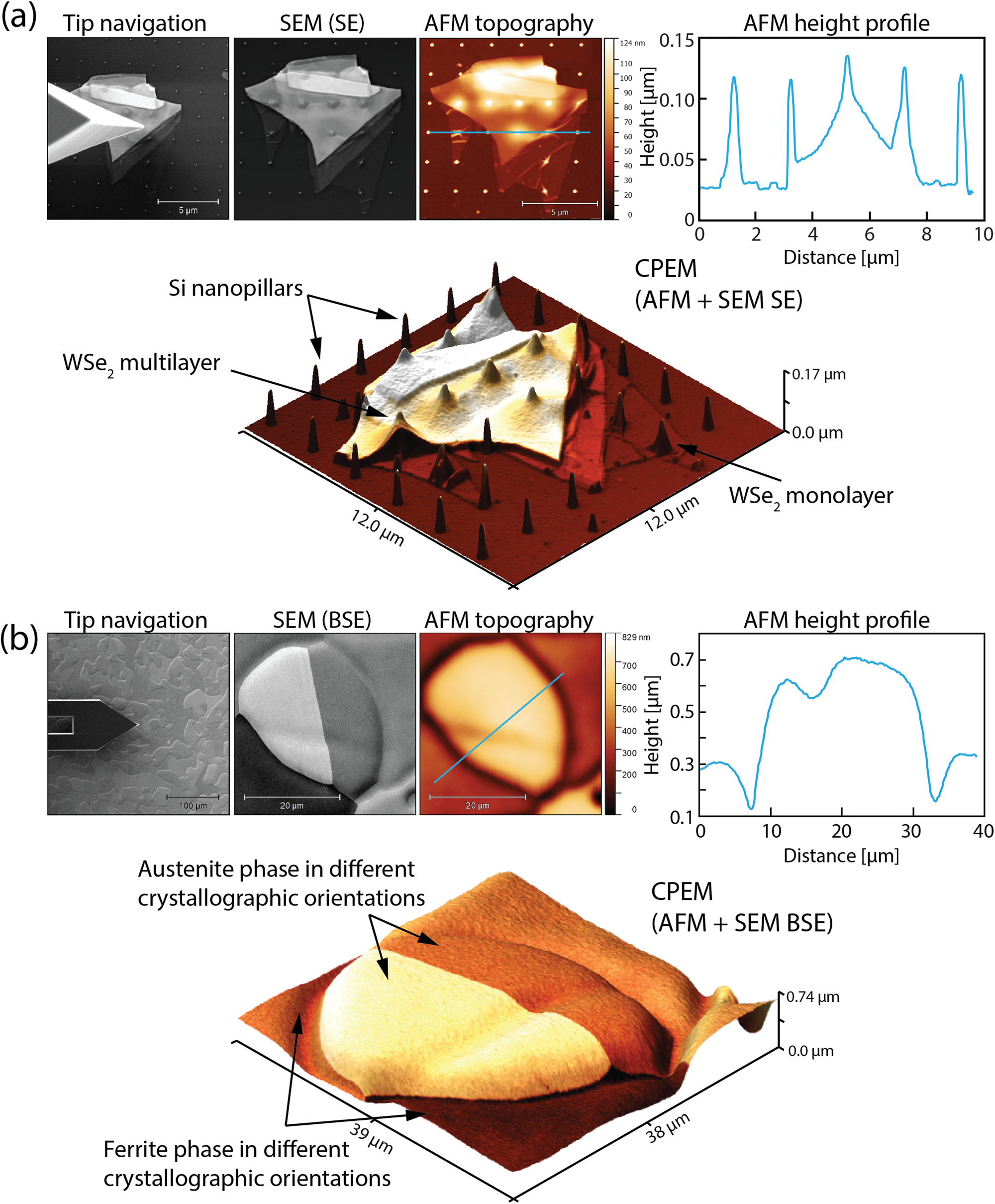
Figure 3: (a) Exfoliated WSe2 flakes on Si nanopillars: overview of the sample in contact with the AFM probe illustrating tip navigation. The signal from the SE detector, AFM topography with height profile, and 3D CPEM view of AFM topography and SE signal. (b) Ferritic-austenitic duplex steel: overview of the sample in contact with the AFM probe. The signal from the BSE detector, AFM topography with height profile, and 3D CPEM view of AFM topography and BSE signal.
Figure 3b shows a sample of ferritic-austenitic duplex steel. This material exhibits improved material and thermal properties in comparison with either completely ferritic or austenitic steel. This results in higher strength with high ductility, outstanding corrosion-resistance properties, higher impact value, and better conductivity [Reference Knyazeva and Pohl12]. Nevertheless, failure in duplex steel processing can modify the balance of alloying elements, which leads to a drastic deterioration of its advantageous properties [Reference Rocha and Duriagina13].
Features of duplex steel are difficult to identify by a single technique. SEM signals visualize the difference in crystallographic orientation of the twin grains within the same austenite phase and surrounding ferrite matrix. However, the duplex steel alloy consists of two phases that are only partially dependent on morphology. The SEM images show only the edges of the grains, but information about grain topography is missing. Simultaneously acquired AFM images provide data of the true surface topography. The scalable 3D CPEM view combines crystallographic contrast and surface morphology, enabling easier interpretation of the surface with high resolution in all three dimensions. Information about topography enables precise measurement of the height and depth of surface structures as well as estimation of the sample roughness.
In situ Sub-Nanometer Profiling and 3D Topography
AFM-in-SEM technology facilitates precise measurement of height and depth of surface structures in SEM applications. It can be operated in a tilted position up to 60°, which makes it compatible with a FIB and gas injection system. This technique is used for surface polishing, sputtering, etching, depositing, or patterning. The results can be immediately viewed by SEM, however, the detailed information about the surface morphology of sputtered or deposited material requires AFM analysis, typically ex situ. The AFM integrated into the FIB-SEM system provides a fast and accurate in situ analysis of the modified surface without the need for sample transfer to another instrument and without changing the environment and breaking the vacuum. Thus, the AFM-in-SEM system in combination with CPEM facilitates FIB process optimization.
Applications for FIB surface modification are depicted in Figure 4, which shows a metastable Fe78Ni22 thin film grown on a Cu(100) substrate whose magnetic properties can be selectively changed when irradiated by an ion beam (direct FIB writing). This material has the potential for magnetic patterning as it is paramagnetic (fcc) at room temperature but can be transformed by FIB irradiation into a ferromagnetic material (bcc) [Reference Urbánek14]. To identify the ion dose intensity causing the fcc-bcc material transformation, an array of FIB milled squares was prepared, as depicted in Figure 4a. The change in material crystallography is detailed in the SEM image in Figure 4b (ion dose intensity of 4.8 × 10¹⁵ ions/cm2). Simultaneous measurement of AFM and SEM signals revealed that the crystallography transformation was accompanied by a topography change with the step between low and high magnetic moment approximately 470 pm, as shown in the height profile in Figure 4c. Additionally, the in situ AFM-in-SEM arrangement was crucial in this study since the Fe78Ni22 represents a sensitive sample where the sample surface is prone to immediate oxidation upon air exposure.
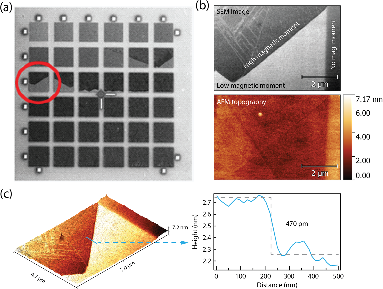
Figure 4: Metastable Fe78Ni22 thin film on Cu(100) substrate. (a) An array of FIB-milled squares (5 × 5 µm each) prepared using different ion dose intensities. The highlighted area shows the partial material crystallography transformation detailed in the SEM image and corresponding AFM topography (b), and combined 3D CPEM view (c) with a topographical step between the high and low magnetic moment.
Measurement of Mechanical Properties
Mechanical properties of a material describe its behavior under loading, and LiteScope offers a variety of methods for measurement of mechanical properties (Table 1). The most studied mechanical properties are stiffness, elasticity, and hardness [Reference Sundararajan15]. The knowledge of these properties is crucial for design, modeling, and analysis of mechanical systems as well as for applications in life sciences. The analysis of mechanical properties on a nanometer scale by multiple techniques provides information about the texture, crystallography, morphology, and properties of individual components and helps to understand the behavior of these systems in the macroscopic world.
A two-component polymer sample, containing polystyrene (PS) and low-density polyethylene (LDPE), was used to demonstrate some capabilities for estimation of mechanical properties; for this purpose, LiteScope is showcased as a stand-alone AFM. Figure 5a shows the topography of the surface with circular regions embedded into a matrix, which can be well correlated with the sample mechanical properties acquired by energy dissipation, FMM, and force-distance curves (Figure 5c). Energy dissipation and FMM provides qualitative information, and both techniques clearly showed a difference in stiffness between the harder PS matrix and the softer, embedded LDPE regions. In general, energy dissipation information is read from the drive signal amplitude in tapping mode and is useful as an alternative to FMM, which uses contact mode AFM. Thus, the application is suitable for samples whose topography is best measured using non-contact mode. In FMM, the AFM tip is scanned in contact with the sample, and an additional driving signal is applied to vibrate the tip, which is converted to a signal used for analysis. Either change in amplitude (data not shown) or phase shift (called phase detection microscopy [PDM]) is used to generate the FMM image. Acquired data can be viewed in 3D, where the topography together with the mechanical properties improves insight into the surface structure (Figure 5b).
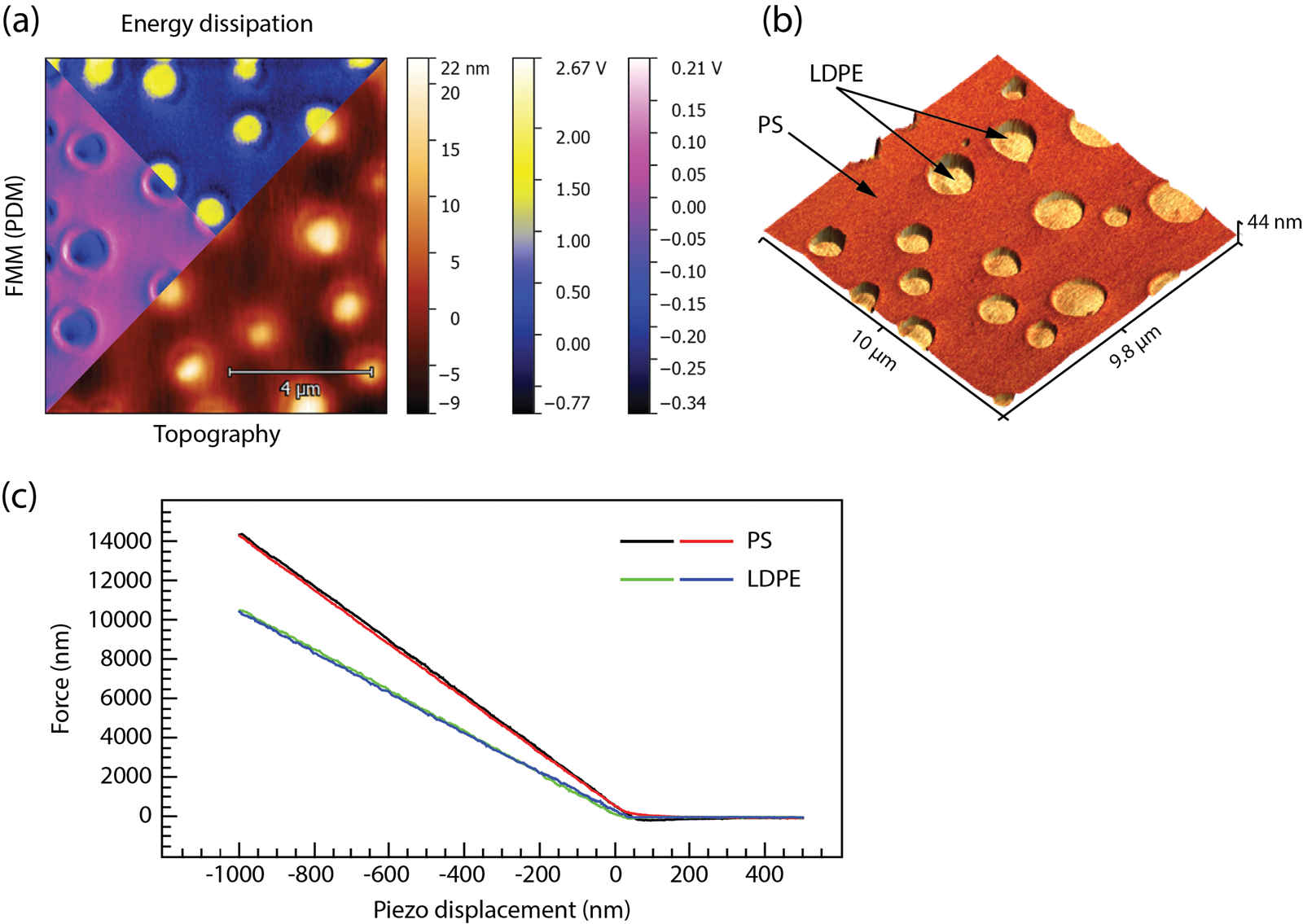
Figure 5: Mechanical properties of the two-component PS and LDPE sample. (a) Sample region showing topography, energy dissipation, and FMM (PDM) image. (b) 3D correlative view showing topography combined with PDM. (c) Difference in slope of force-distance curves demonstrates differences in relative hardness of the PS and LDPE components.
On the other hand, force-distance curves (or F/z spectroscopy) provide a quantitative estimation of the local mechanical property by measuring the vertical force between the AFM tip and the surface, and the sample displacement. It is used for many purposes including sample stiffness analysis, detailed surface-tip force progress, and local elasticity/plasticity determination. The curves (and the slopes) in Figure 5c show a clear difference between the components of the polymer blend with the established material hardness of 2 GPa for PS and 0.3 GPa for LDPE.
The advantages of combining related techniques into one tool are further demonstrated on the nanoindentation of M3 class 2 high-speed steel, which is used in the automotive industry [Reference Randall16]. In general, nanoindentation represents an extremely versatile technique to determine material mechanical properties at the nanoscale such as elastic modulus, hardness values, fracture toughness, or creep and yield stress. In this case, the AFM-in-SEM approach was further extended by adding a nanoindenter [17] to the scan head. This hybrid technique enables sample phase identification, precise indentation targeting, and topographical analysis all in one measurement.
Figure 6 shows the etched steel nanoindentation analysis results. The SEM images (Figure 6a) showed a wide range of separate phases of small size (MnS grain, carbide M6C, and martensitic matrix), that were nanoindented using a force of 15 mN. The AFM scans in Figure 6b revealed that each phase reacted differently to the acting force. The softest material is the MnS grain, followed by a matrix, and the hardest is the M6C part of the composite, as depicted in the height profile in Figure 6c. The detailed 3D AFM view shows indentation in the matrix with the amount of material pushed out of the indent (the black arrows in Figures 6c and 6d).
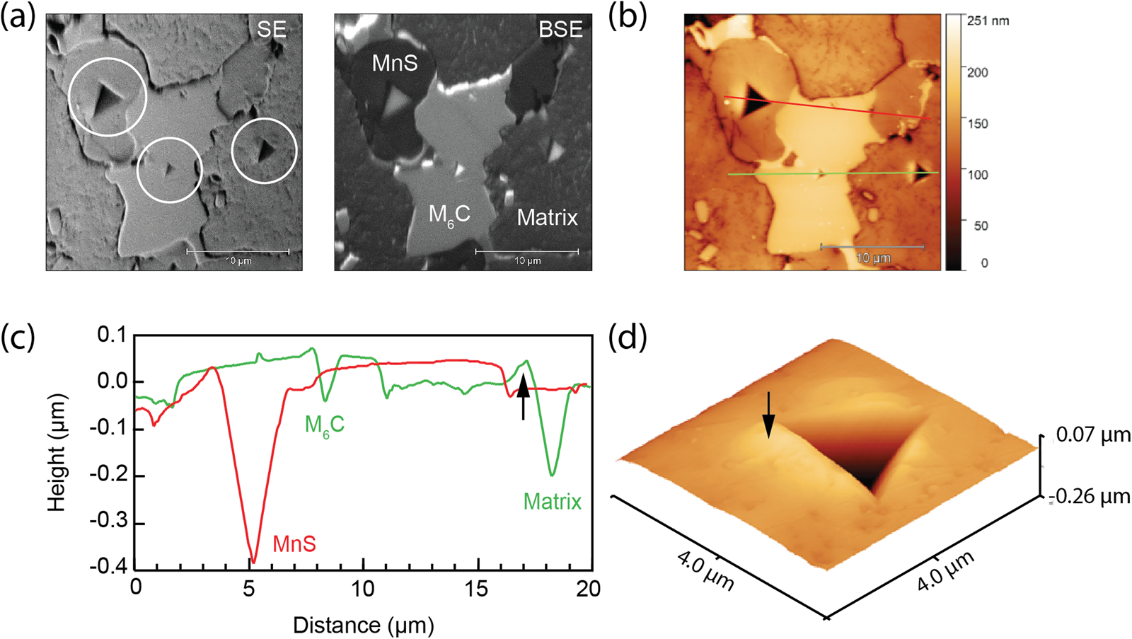
Figure 6: Mechanical properties of an M3 class 2 high speed steel. (a) SE image with circles highlighting individual indents and BSE image indicating the material composition. (b) AFM topography image with profile lines detailed in the depth profile (c) and (d) 3D AFM view of indentation in the matrix. The arrows in (c) and (d) highlight the same area.
Measurement of Electrical Properties
The measurement of electrical properties can also be carried out. This category includes conductive AFM (C-AFM), conductive CPEM (C-CPEM), Kelvin probe force microscopy (KPFM), probe force microscopy PFM, and spectroscopy regimes (Table 1). Technical advancement, especially in the semiconductor and solar industries, places increasing demand on the measurement of current distribution (conductivity) over the sample surface with nanometer precision. Conductive AFM represents a common technique where a bias voltage is applied between the conductive cantilever and the sample, and the resulting current (as well as topography) is measured as the tip scans the sample surface. Clearly, this approach cannot work in insulated areas (Figure 7a), as depicted in Figure 7b. However, this C-AFM limitation can be overcome by the AFM-in-SEM approach combined with C-CPEM technology (Figure 7c), where the electron beam at the constant distance from the tip replaces the need for an applied bias in the measured area, and the tip-sample bias can still be simultaneously applied. During scanning, the tip-sample current flow is measured in contact AFM mode. This means that during a single measurement, information about the sample topography in contact mode, SE and BSE images, and a conductivity map can be acquired.
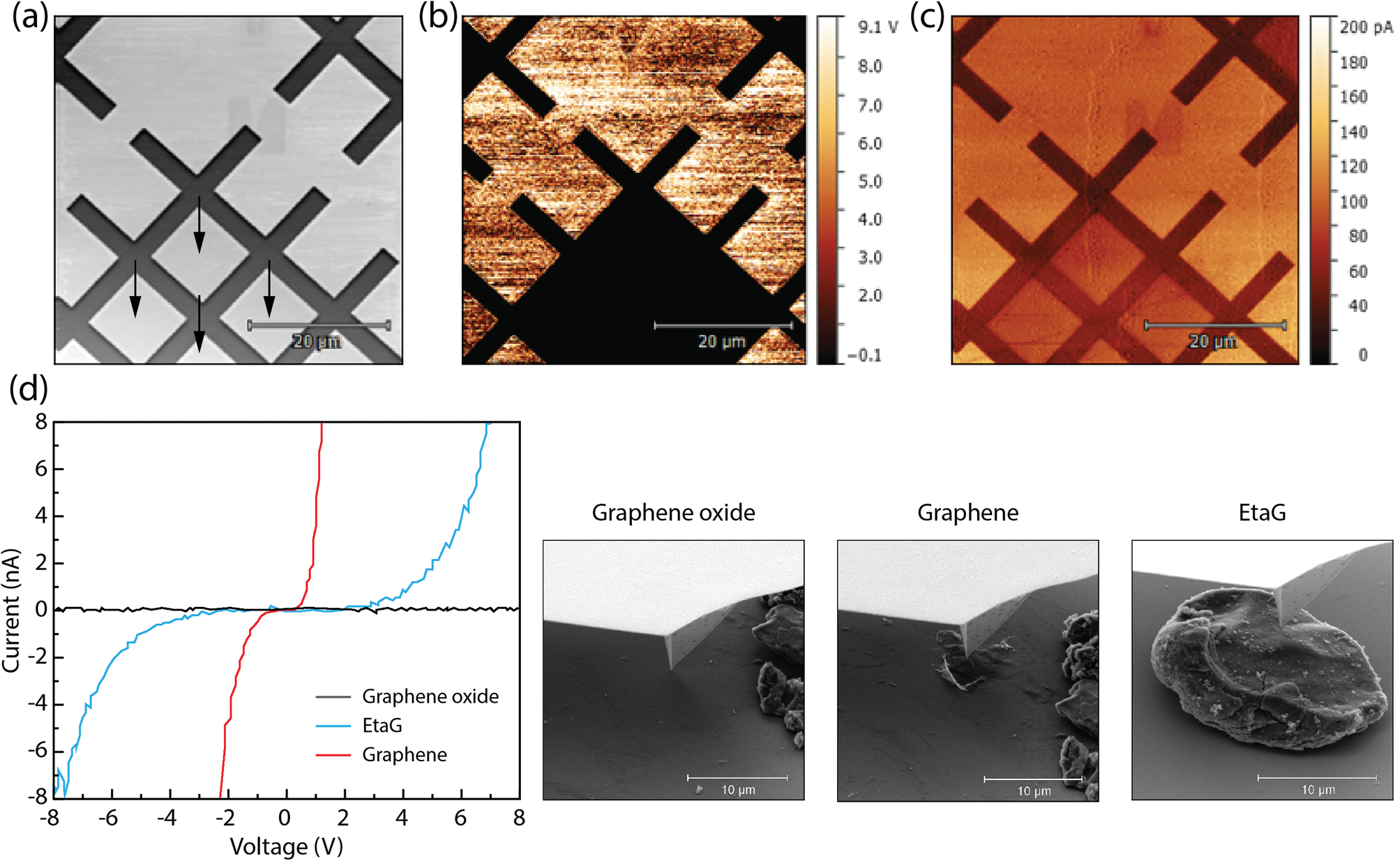
Figure 7: C-CPEM and I/V curves. The same sample area imaged by SEM (a) showing the insulated areas (highlighted by arrows) that failed to be visualized in the C-AFM conductivity map (b), but are clearly visible by C-CPEM (c) using the SEM electron beam as a bias source. (d) The I/V curves characterize differences in conductivity on a sample containing graphene oxide, graphene, and EtaG identified by SEM (images show the conductive AFM tip in contact with the corresponding material).
For a detailed local investigation of the surface electrical properties, AFM-in-SEM can be used to measure current-voltage characteristics (I/V curves) by applying a bias of -10V to 10V. Figure 7d demonstrates the use of I/V curves for conductivity measurement of a sample containing graphene oxide, graphene, and 4-ethynylaniline graphene derivative (EtaG). The SEM enables precise identification and navigation of the conductive tip to the respective material. The investigation revealed that graphene oxide is non-conductive, EtaG more conductive, and graphene the most conductive material [Reference Chronopoulos18].
Conclusion
This article provides insight into the AFM-in-SEM technology. The LiteScope is a compact, yet powerful, AFM that fits into a large variety of SEM systems in a plug-and-play fashion. It provides complex sample surface analysis by supporting multiple techniques measuring structural, electrical, magnetic, and mechanical properties. The unique CPEM technology allows a number of AFM and SEM signals to be simultaneously measured and automatically correlated into one detailed 3D image while maintaining the same pixel size and coordinate system. The described technology enables complex sample analysis that was either impossible or extremely tedious/expensive when measured by separate instruments.
Using the SEM to navigate the AFM tip with nanometer precision provides quick localization and study of nanostructures and nanodevices of interest, making analysis precise, comprehensive, and time- and cost-efficient. Combined with FIB, AFM-in-SEM technology offers a range of measurements that are impossible to do with separate stand-alone devices or by other techniques. Additionally, this opens up new possibilities for advanced measurements in the field of metrology, FIB milling optimization, and electron beam induced current or spectroscopy analysis where the combination of AFM and SEM is essential. However, these applications are beyond the scope of this article.
Taken together, the main advantages of the LiteScope are a compact design compatible with most SEM systems, simultaneous in situ measurement of multiple signals, addition of 3D information to 2D SEM images, a variety of self-sensing and self-actuating probes without laser detection, fast and precise navigation of the probes to the ROI by SEM, a plethora of measurement techniques for comprehensive sample analysis, and web-based software.
Acknowledgments
This article was created with state support from the Technology Agency of the Czech Republic within the Program for the Support of Applied Research ZÉTA for the project Development of SPM applications suitable for correlative microscopy, project number TJ01000434. The authors also thank all researchers who prepared and provided samples for the analysis.


