


Introduction
The scanning transmission electron microscope (STEM) is an exceptionally powerful instrument for materials characterization. By forming an electron probe at the sample, a plethora of spatially localized transmitted, reflected, or emitted imaging and spectroscopic signals are available simultaneously to the operator. Of these signals, annular dark-field, bright-field, or annular bright-field (ADF, BF, or ABF, respectively) are some of the most popular imaging techniques. Each of these modalities is commonly realized using a scintillator–photomultiplier style detector which collects a particular scattering angle range within the detector plane. The electron-flux falling on the scintillator leads to a voltage at the photomultiplier (PMT) which is expressed as a function of position to yield an image. However, more information per scan point can be captured when using a pixelated detector instead of an integrating detector. While early implementation of this “4D-STEM”—in which reciprocal space is sampled in two dimensions (2D) while real space is scanned in 2D—happened already in the early 2000s (Zaluzec, Reference Zaluzec2002; Rauch & Duft, Reference Rauch and Duft2005), the slow speed of the cameras at that time limited the spread of this technique or the real-space field-of-view (Kimoto & Ishizuka, Reference Kimoto and Ishizuka2011). Recent advances in fast electron sensors now allow for pixelated detectors to acquire data 10–100 times faster than slow scan charge-coupled devices. A trivial use of these new sensors would be to synthesize the existing imaging modes previously available; however, the abundance of information available in a 4D-STEM data set has enabled a variety of imaging and reconstruction techniques to be practically realized. These applications include mapping crystalline orientation (Rauch et al., Reference Rauch, Portillo, Nicolopoulos, Bultreys, Rouvimov and Moeck2010; Seyring et al., Reference Seyring, Song and Rettenmayr2011; Kobler et al., Reference Kobler, Kashiwar, Hahn and Kübel2013; Izadi et al., Reference Izadi, Darbal, Sarkar and Rajagopalan2017), mapping electric fields (Müller et al., Reference Müller, Krause, Béché, Schowalter, Galioit, Löffler, Verbeeck, Zweck, Schattschneider, Rosenauer, Müller-Caspary, Krause, Béché, Schowalter, Galioit, Löffler, Verbeeck, Zweck, Schattschneider and Rosenauer2014; Müller-Caspary et al., Reference Müller-Caspary, Krause, Grieb, Löffler, Schowalter, Béché, Galioit, Marquardt, Zweck, Schattschneider, Verbeeck and Rosenauer2017; Gao et al., Reference Gao, Addiego, Wang, Yan, Hou, Ji, Heikes, Zhang, Li, Huyan, Blum, Aoki, Nie, Schlom, Wu and Pan2019), and magnetic domains (Krajnak et al., Reference Krajnak, McGrouther, Maneuski, O'Shea and McVitie2016; Tate et al., Reference Tate, Purohit, Chamberlain, Nguyen, Hovden, Chang, Deb, Turgut, Heron, Schlom, Ralph, Fuchs, Shanks, Philipp, Muller and Gruner2016), using center-of-mass (COM) approaches (Müller et al., Reference Müller, Krause, Béché, Schowalter, Galioit, Löffler, Verbeeck, Zweck, Schattschneider, Rosenauer, Müller-Caspary, Krause, Béché, Schowalter, Galioit, Löffler, Verbeeck, Zweck, Schattschneider and Rosenauer2014; Lazić et al., Reference Lazić, Bosch and Lazar2016), and performing phase reconstruction techniques such as electron ptychography (Rodenburg et al., Reference Rodenburg, McCallum and Nellist1993; Nellist et al., Reference Nellist, McCallum and Rodenburg1995; Pennycook et al., Reference Pennycook, Lupini, Yang, Murfitt, Jones and Nellist2015). More past and current applications of 4D-STEM and related hardware can be found in reviews by Ophus (Reference Ophus2019) and MacLaren et al. (Reference MacLaren, MacGregor, Allen and Kirkland2020).
In recent years, both ptychography and COM-imaging have become of especial interest for imaging of light and thin specimens, where absorption contrast may be very weak, at up to atomic resolution. The object phase may carry information about the sample potential, electric field, and atomic resolution polarization. Focused-probe STEM ptychography approaches have already demonstrated a variety of novel applications, such as visualizing lithium in cathode materials (Lozano et al., Reference Lozano, Martinez, Jin, Nellist and Bruce2018), imaging beam-sensitive zeolites at atomic resolution (O'Leary et al., Reference O'Leary, Allen, Huang, Kim, Liberti, Nellist and Kirkland2020), optical-sectioning of carbon-based nanostructures (Yang et al., Reference Yang, Rutte, Jones, Simson, Sagawa, Ryll, Huth, Pennycook, Green, Soltau, Kondo, Davis and Nellist2016), and increasing the resolution beyond that of conventional STEM images (Jiang et al., Reference Jiang, Chen, Han, Deb, Gao, Xie, Purohit, Tate, Park, Gruner, Elser and Muller2018), even when severely binning the data for achieving high scan speeds (Schloz et al., Reference Schloz, Pekin, Chen, Van den Broek, Muller and Koch2020). COM analysis of atomic-resolution 4D-STEM data has been utilized in equally diverse applications, including the identification of surface adatoms (Wen et al., Reference Wen, Ophus, Allen, Fang, Chen, Kaxiras, Kirkland and Warner2019) and the determination of charge accumulation at interfaces (Gao et al., Reference Gao, Addiego, Wang, Yan, Hou, Ji, Heikes, Zhang, Li, Huyan, Blum, Aoki, Nie, Schlom, Wu and Pan2019).
4D-STEM detectors need not wholly replace conventional hardware and can be installed co-operatively to record the beam which passes through the center of an annular detector. This configuration, along with the additional flexibility of variable camera-lengths, allows for the simultaneous acquisition of multiple detector signals. For example, by acquiring ADF and ptychographic data simultaneously, both light and heavy elements can be identified using data from a single experimental STEM scan (Yang et al., Reference Yang, Rutte, Jones, Simson, Sagawa, Ryll, Huth, Pennycook, Green, Soltau, Kondo, Davis and Nellist2016). Furthermore, spectroscopic data can be acquired simultaneously to 4D-STEM and annular detector imaging by using an off-axial detector.
High-resolution TEM focal/tilt series restoration (HRTEM-FTSR) offers one route to fusing contrast transfer functions and achieving phase-imaging (Meyer et al., Reference Meyer, Kirkland and Saxton2002, Reference Meyer, Kirkland and Saxton2004). However, it requires the precise lateral registration of defocused frames and contrast reversals mean this remains a challenging task. With 4D-STEM approaches, all beam-angles (tilts) are recorded simultaneously, and a phase image can be reconstructed from a single scan frame. However, as discussed, the trade-off is the risk of line-by-line scanning instability which HRTEM is not affected by in the same way.
In the STEM, unlike a conventional transmission electron microscope (CTEM), a raster scan is required to build up a 2D image or chemical map. The sequential nature of this serial-scan opens the STEM to the potential weakness of imperfect environmental stability during the time needed to record each scan frame. These instabilities might be acoustic, seismic, thermal, barometric, electronic, or magnetic in nature and should be kept to an absolute minimum wherever possible through good instrument and suite design (Muller & Grazul, Reference Muller and Grazul2001; Muller et al., Reference Muller, Kirkland, Thomas, Grazul, Fitting and Weyland2006). In this manuscript, although the approach followed is general, we will consider the case of atomic-resolution STEM, as the high magnification presents the worst-case scenario for scan-distortions.
In the data, these artifacts manifest themselves in a variety of ways; stage movements between frame-captures appear as a simple rigid-translation, whereas continual stage-drift within a frame's recording time (but still slow with respect to the frame time, e.g., <¼ period per frame time) will add an affine shearing to the image data (Rahe et al., Reference Rahe, Bechstein and Kühnle2010; Jones & Nellist, Reference Jones and Nellist2013; Sang & LeBeau, Reference Sang and LeBeau2014). Slightly faster stage movements or environmental distortions, with periods ranging from around 1 cycle-per-frame up to several tens of cycles-per-frame, will appear as an irregular non-linear warping whose shifts are characteristically highly correlated along the fast-scan direction (Sun & Pang, Reference Sun and Pang2006; Jones et al., Reference Jones, Yang, Pennycook, Marshall, Van Aert, Browning, Castell and Nellist2015; Ophus et al., Reference Ophus, Ciston and Nelson2016; Wang et al., Reference Wang, Eren Suyolcu, Salzberger, Hahn, Srot, Sigle and van Aken2018). Higher-frequency instabilities can also arise in the microscope lab, but these can be relatively easily damped with the use of instrument enclosures or heavy curtains.
Unfortunately, even with the newest generation of fast pixelated STEM sensors, the pixel times (and hence frame rates) for 4D-STEM may be 100–1,000 times slower than simple integrating type detectors (Gao et al., Reference Gao, Addiego, Wang, Yan, Hou, Ji, Heikes, Zhang, Li, Huyan, Blum, Aoki, Nie, Schlom, Wu and Pan2019). This results in the distortion frequencies of interest being slower by the same ratio, more challenging to shield or damp in hardware, and almost unavoidable in experimental data.
In this manuscript, we propose a multi-frame acquisition and data registration strategy to compensate for the effects of scanning distortions in 4D-STEM. By acquiring multiple frames and subsequently aligning them, both the spatial precision and signal-to-noise ratio (SNR) of the data can be improved. This, in turn, improves the quality of the reconstructions obtained from 4D-STEM imaging and analysis techniques such as electron ptychography and center-of-mass imaging.
The remainder of this manuscript is structured as follows: firstly, the frequency ranges of scanning-distortion most deleterious to atomic-resolution 4D-STEM mapping will be introduced. This is followed by a discussion of the data acquisition and non-rigid correction techniques used to mitigate these scanning-distortions. Next, we present two example applications of the proposed workflow: multi-frame electron ptychography and COM imaging of monolayer, bi-layer, and bulk-like crystalline materials. Following this, a discussion of the attained spatial resolution and phase/field precision will be presented. Finally, the potential applications of this correction approach will be discussed.
Background
In addition to the imaging and diffraction capabilities of the STEM, various spectroscopic modes are also available, such as energy-dispersive X-ray spectrometry (EDX) and electron energy-loss spectroscopy (EELS). Although annular image detectors, EDX spectrometers, and EELS systems can be used to acquire data simultaneously, the optimal acquisition times for each technique are not identical.
Typical frame times of conventional STEM imaging range from one second to a few tens of seconds. As a result, these scans can be vulnerable to high-frequency “scan-noise” (Fig. 1, ~100 Hz up to few kHz) and software corrections for this have been proposed (Sanchez et al., Reference Sanchez, Galindo, Kret, Falke, Beanland and Goodhew2006; Braidy et al., Reference Braidy, Le Bouar, Lazar and Ricolleau2012; Jones & Nellist, Reference Jones and Nellist2013). Alongside these software tools, improved efforts in the construction of microscope rooms (such as heavy curtains, vibration damping systems, and electromagnetic shielding/compensation) and from instrument manufacturers to better block barometric fluctuations and acoustic noise (such as the goniometer “clamshell” or full enclosures) have largely solved this issue.

Fig. 1. Comparison of the frequency ranges of various scan-induced data artifacts and the associated correction methodologies. For the slower recording strategies, the same manifestations are shifted down to lower frequencies.
However, for spectroscopic acquisitions, either because of hardware limitations or simply to collect enough signal, pixel times and hence frame times are often 1–2 orders of magnitude larger than for conventional STEM imaging. As a result, the frequencies that instruments are susceptible to are shifted lower and many operators will be familiar with this when recording spectral maps. Typical frequency ranges for imaging and spectroscopy are shown in Figure 1.
For fully pixelated STEM sensors, the readout rate is again another order of magnitude or more slower. Typical readouts may be only 1 k–8 k frames per second (where now one frame refers to one STEM probe position). Thus, electron ptychography may be susceptible to environmental and instrumental distortions as slow as 1 mHz. Even with the advent of faster detector technology, the limited dynamic range of many fully pixelated STEM sensors places restrictions on the maximum SNR obtainable for a single data set. Thus, there is currently a need for data registration of multi-frame 4D-STEM data.
Fortunately, the correction of scanning distortion has received significant study which can be repurposed for this new field. The scanned physical-probe community [including atomic-force microscopy (Sun & Pang, Reference Sun and Pang2006) and scanning-tunneling microscopy (Rahe et al., Reference Rahe, Bechstein and Kühnle2010; Jones et al., Reference Jones, Wang, Hu, ur Rahman and Castell2018b)] have each developed techniques for remedying imperfect scanning. More recently, the electron imaging community has developed similar tools to push the instrumentation into the picometre spatial-precision regime (Berkels et al., Reference Berkels, Binev, Blom, Dahmen, Sharpley and Vogt2014; Sang & LeBeau, Reference Sang and LeBeau2014; Jones et al., Reference Jones, Yang, Pennycook, Marshall, Van Aert, Browning, Castell and Nellist2015).
Of these techniques, the most applicable in the context of 4D-STEM are the ones that deal with higher-dimensional data (Yankovich et al., Reference Yankovich, Zhang, Oh, Slater, Azough, Freer, Haigh, Willett and Voyles2016; Wang et al., Reference Wang, Eren Suyolcu, Salzberger, Hahn, Srot, Sigle and van Aken2018; Jones et al., Reference Jones, Varambhia, Beanland, Kepaptsoglou, Griffiths, Ishizuka, Azough, Freer, Ishizuka, Cherns, Ramasse, Lozano-Perez and Nellist2018a), and those which can compensate for fully non-linear scanning corrections (not just affine). To extend these techniques, we first take a moment to consider the data-dimensionality, as illustrated in Figure 2.

Fig. 2. Schematic of the dimensionality of various STEM data types. Conventional integrating-type imaging detectors such as BF, ADF, or ABF, (a) yield two-dimensional (2D) data. Spectroscopic techniques such as EELS or EDX add an energy dimension to this (b). Spatially resolved diffraction or ptychographic recordings with pixelated sensors record four-dimensional data (c). For all these techniques, multiple scan-frames may be recorded to form a series, in which case the dimensionality of the data is increased by 1.
For conventional imaging (BF, ADF, etc.), a 2D array of values is recorded as a function of probe position. There may be two or more of these detectors in use simultaneously, but each of these represents only one 2D array. Spectrum imaging increases this data dimensionality to the third dimension by adding some energy axis. In this case, an additional spectrum dimension is recorded at every probe position in the 2D raster scan. The dimensionality of this is then the same as the case of energy-filtered TEM imaging (EFTEM), but here we concentrate on the scanned case. In such “spectrum volumes,” every energy “slice” in our scanned data volume has the same lateral real-space distortions and this is key to their eventual correction (Yankovich et al., Reference Yankovich, Zhang, Oh, Slater, Azough, Freer, Haigh, Willett and Voyles2016; Jones et al., Reference Jones, Varambhia, Beanland, Kepaptsoglou, Griffiths, Ishizuka, Azough, Freer, Ishizuka, Cherns, Ramasse, Lozano-Perez and Nellist2018a).
4D-STEM, as the name suggests, takes this one dimension further, with every real-space probe position corresponding to a 2D image in the camera plane. If the time dimension of the series is also counted, this 4D series may be considered as a single overall 5D data set. Analogous to registering a series of spectrum images, the 5D data set will be registered in the two spatial dimensions and then projected along the time dimension into an improved 4D-STEM data set. The complication is now that the detector signal is not a scalar, but a 2D array of pixel values in the momentum plane of the detector.
For each pixel in this camera plane, TEM-STEM reciprocity allows us to visualize this as a series of tilted illumination images all recorded simultaneously (Lupini et al., Reference Lupini, Chi and Jesse2016), where each tilted image possesses an identical real-space field-of-view and real-space scan-distortions. Additionally, this same reciprocity argument allows us to reshape the 4D array down to only three dimensions, where the third dimension now represents just a pixel-indexing number corresponding to that series of tilted images as each tilt can be processed as an independent data set (Fig. 2).
Once the data are reshaped, they can be distortion-corrected using the existing approach followed by the SmartAlign algorithm (Jones et al., Reference Jones, Yang, Pennycook, Marshall, Van Aert, Browning, Castell and Nellist2015, Reference Jones, Varambhia, Beanland, Kepaptsoglou, Griffiths, Ishizuka, Azough, Freer, Ishizuka, Cherns, Ramasse, Lozano-Perez and Nellist2018a). This approach differs from some others in that it is not limited to affine only correction (Sang & LeBeau, Reference Sang and LeBeau2014), does not require atomic-column peaks for distortion analysis (Wang et al., Reference Wang, Eren Suyolcu, Salzberger, Hahn, Srot, Sigle and van Aken2018), and does not require all the data to be opened in RAM simultaneously during the distortion correction (Yankovich et al., Reference Yankovich, Zhang, Oh, Slater, Azough, Freer, Haigh, Willett and Voyles2016). Furthermore, the scan diagnosis is compatible using data both with or without 90° scan-rotation increments (Sang & LeBeau, Reference Sang and LeBeau2014; Ophus et al., Reference Ophus, Ciston and Nelson2016).
After correction of this series of 3D data sets, they are reshaped back into a series of 4D data items and can be projected along (summed over) the series dimension to obtain an improved 4D-STEM data item or looked at individually as a registered time series of 4D-STEM. In the following, we will concentrate on the former option to show the improved characteristics of the projected 4D map, but the subsequent processing of the data after registration is the same in all cases and equal to a conventional 4D-STEM data set.
After correction, the data are reshaped back from the 3D form to the 4D form for onward processing with the researcher's choice of phase- or field-reconstruction algorithm (Pennycook et al., Reference Pennycook, Martinez, O'Leary, Yang and Nellist2019; Clausen et al., Reference Clausen, Weber, Ruzaeva, Migunov, Baburajan, Bahuleyan, Caron, Chandra, Halder, Nord, Müller-Caspary and Dunin-Borkowski2020; Savitzky et al., Reference Savitzky, Hughes, Zeltmann, Brown, Zhao, Pelz, Barnard, Donohue, DaCosta, Pekin, Kennedy, Janish, Schneider, Herring, Gopal, Anapolsky, Ercius, Scott, Ciston, Minor and Ophus2020).
Methods
In this work, multi-frame 4D data acquisition and registration is demonstrated for two 4D-STEM imaging techniques: (1) center-of-mass (COM) imaging and (2) non-iterative electron ptychography.
The COM E-field data was recorded using a Nion HERMES microscope located at Humboldt-Universität zu Berlin. The microscope was operated at 60 kV for each of the three examples.
The gadolinium aluminum gallium garnet (GAGG) data shown in Figures 3 and 5 was acquired with a convergence angle of 36 mrad and an ADF inner-angle of 60 mrad, 128 × 128 detector pixels (windowed region of a 2,048 × 2,048 fiber-coupled Hamamatsu ORCA SCMOS camera) running at 1,000 frames per second with an angular resolution of 1.2 mrad/pix, 110 × 126 scan points (128 × 128 before registration) with a sampling of 0.313 Å and a beam current of 43 pA.

Fig. 3. Individual Ronchigrams extracted from a column position (blue) and a position in between columns (orange) of a single 4D map (a) and the sum of a non-rigid registration (b) from a gadolinium aluminium gallium garnet (GAGG) sample. The positions are indicated with stars in the corresponding HAADF images in the center. The pink dashed line indicates the position of the profiles that are also plotted in pink and illustrate the reduction of noise in the fused data compared with a single map. The data set is the same as in Figure 5.
In the case of the WS2 sample shown in Figure 4, the data were obtained using a convergence angle of 35 mrad with the same ADF inner-angle, 4D detector angular resolution, and windowing as before but running at 1,600 frames per second, 68 × 96 scan points (128 × 128 before registration) with the same sampling but a current of 28 pA.

Fig. 4. Comparison of single 4D map (a) and six fused (non-rigidly registered) data sets (b) of a WS2 monolayer with two defects: virtual ADF image (left), E-field map (center), and charge-density distribution (right).

Fig. 5. Single 4D data set (a) and sum of ten (non-rigidly) registered maps (b) of a gadolinium aluminium gallium garnet (GAGG). Depicted are virtual ADF images (left), color-coded E-field map (center), and projected charge density (right).
For the twisted bilayer graphene sample, the data were acquired with a convergence angle of 40 mrad and an ADF inner-angle of 50 mrad, a windowed 256 × 256 pixel detector region (binned by 4 to 64 × 64 pixels) of the prototype Dectris ELA direct detector (1,030 × 514 pixels) (Plotkin-Swing et al., Reference Plotkin-Swing, Corbin, De Carlo, Dellby, Hoermann, Hoffman, Lovejoy, Meyer, Mittelberger, Pantelic, Piazza and Krivanek2020) running at 4,000 frames per second with an angular resolution of 2.5 mrad/pix, 219 × 189 scan points (256 × 256 before registration) with a sampling of 0.156 Å and a beam current of 85 pA.
The ptychographic data was recorded using a JEOL ARM200CF at the David Cockayne Centre for Electron Microscopy. A JEOL 4DCanvas fast pixelated detector (264 × 264 pixels) was used, which was operated at 4,000 frames per second with fourfold binning (66 × 264 pixels) (Ryll et al., Reference Ryll, Simson, Hartmann, Holl, Huth, Ihle, Kondo, Kotula, Liebel, Müller-Caspary, Rosenauer, Sagawa, Schmidt, Soltau and Strüder2016). The microscope was operated at 80 kV with a 31 mrad probe semi-convergence angle and 16 pA beam current resulting in a dose of approximately 3.5 × 10⁵ eÅ−2 per scan frame. A series of 21 frames were recorded of both pixelated STEM data and hardware-ADF images, resulting in a cumulative dose of 7.35 × 10⁶ eÅ−2. The real-space dimensions are 246 × 225 scan points (256 × 256 before registration) with a probe step size of 0.264 Å. The ptychographic phase reconstructions were obtained using the single-side-band method (Pennycook et al., Reference Pennycook, Lupini, Yang, Murfitt, Jones and Nellist2015).
Using the physical-ADF signal for the registration and distortion diagnosis is convenient so long as there is adequate dark-field signal in each image. However, for the WS2, GAGG, twisted bilayer, and ptychography data sets, these diagnoses were all performed using the virtual-ADF series synthesized from the 5D data. This alternative method is advantageous for two reasons. First, the virtual detector geometry can be optimized after acquisition to maximize the signal available for the image registration process. If the sample signal is weak at high scattering angles, a bright-field or DPC detector geometry can be assumed to generate a raw image series which can be used as input to the registration algorithm. Second, any synchronization issues between separate detectors can be avoided.
The drift and distortion diagnosis were performed using the SmartAlign algorithm (Jones et al., Reference Jones, Yang, Pennycook, Marshall, Van Aert, Browning, Castell and Nellist2015), where importantly, the x–y sample shifts and the scan-distortion vector fields are stored after the calculation is complete. The SmartAlign algorithm is described in detail elsewhere, but briefly, this approach involves comparing the intensity difference between the moving image and the reference image. The difference in the local gradients of the images then directs the pixel-wise offsets needed. This diagnosis is performed in an iterative manner until the full distortions are determined (Jones et al., Reference Jones, Yang, Pennycook, Marshall, Van Aert, Browning, Castell and Nellist2015).
Some experimental optimizations may be made to maximize the quality of the eventual registration; for example, a small scan-rotation may be added during acquisition to rotate the low-order planes of the material away from the fast-scan direction. This avoids blank rows with no contrast and allows for more reliable diagnosis and compensation of scan-distortion. Additionally, at the camera-lengths required for the 4D cameras, the physical ADF detector may have a large inner-angle, causing the data to be somewhat noisy. In the case of noisy data due to large ADF inner-angles, gentle bandpass filtering was tried and did not seem to limit the precision of probe-offset vectors and therefore seems to be a viable option to enhance the registration.
In principle, it is possible to correct a single 4D volume for scan-distortion if another reliable reference image is available (such as a fast multi-frame average ADF frame) (Recnik et al., Reference Recnik, Möbus and Sturm2005; Gao et al., Reference Gao, Addiego, Wang, Yan, Hou, Ji, Heikes, Zhang, Li, Huyan, Blum, Aoki, Nie, Schlom, Wu and Pan2019), however by recording these data as an entire series the corrections can be made with no external prior knowledge applied.
Results and Discussion
In this section, we first discuss the process of scan-distortion diagnosis, alignment and subsequent dose fusion and present the obtained new “raw” 4D-STEM data set before discussing the improved quality of results obtained from this data by applying existing COM and ptychography workflows to it.
Alignment and Scan-Distortion Diagnosis
The ADF frames acquired simultaneously to the 4D-STEM data were used for the scan-distortion diagnosis. This process yields a vector field with the same dimensions as each frame, such that the diagnosis provides the x–y vector needed to correct the probe-offset for every pixel over the field-of-view and in every frame. An example of these x–y vector data from one frame of the experimental series is shown in Supplementary Figure S1. For an ADF image, a scan distortion on the scale of a single pixel would be easily visible in a strain analysis but would otherwise be considered qualitatively minor.
As single side-band ptychographic reconstruction relies on Fourier transforms (taken with respect to real space) this spatially distributed distortion becomes a phase corruption in Fourier-space and may significantly affect the precision of both aberration diagnosis and reconstruction (Yang et al., Reference Yang, Rutte, Jones, Simson, Sagawa, Ryll, Huth, Pennycook, Green, Soltau, Kondo, Davis and Nellist2016).
For COM analysis of the data, these distortions are a major problem as the E-field vectors critically rely on the precise position of the probe. This can be rationalized by the fact that the E-field (whose deflecting influence on the probe is directly measured) diverges toward the atom centers and then flips sign on crossing it, which is a distinctly different behavior from other signals that are typically collected. The finer the probe, the more important is a precise knowledge of the (actual) probe position as the (divergent) field is not smeared out so much and leads to a more abrupt change of COM vector on crossing the atom center. Therefore, COM greatly benefits from the registration of 4D series.
Dose-Fusion After Alignment
After rigid translation in real space, the data are cropped to their common field-of-view and then aligned using non-rigid registration. The 4D data sets corrected with the same diagnoses also retain this same field-of-view.
Figure 3 shows example Ronchigrams from both a single 4D data set and a dose-fused data set (registered and integrated) of a GAGG sample. By comparing Ronchigrams from a single 4D map (a) and ten fused maps (b) of a column position (blue) and an off-column position (orange), it can be seen that the dose-fused data has an improved noise level without exhibiting any artifacts from the registration process. Fine details in the Ronchigrams are clearly conserved and the only visible influence of the process is the augmentation of the number of electrons and subsequent reduction of Poisson noise. The enhancement of the data through (sub-pixel) correction of the actual probe position is not fully revealed from this figure but will become evident in the subsequent analyses.
COM Analysis
Here, we present three illustrative examples to show the applicability of the approach; a monolayer material (WS2) and a bulk-like crystal (GAGG) each acquired using an optically coupled CMOS detector, and a twisted bilayer graphene data set acquired using the Dectris ELA prototype direct detector (Plotkin-Swing et al., Reference Plotkin-Swing, Corbin, De Carlo, Dellby, Hoermann, Hoffman, Lovejoy, Meyer, Mittelberger, Pantelic, Piazza and Krivanek2020). Detailed parameters of the data sets can be found in the Methods section.
Figure 4 depicts a virtual ADF image, the color-coded E-field map obtained from the COM analysis and the projected charge density (calculated from the E-field) of a single 4D-STEM data set (a) and of six registered sets (b) of a WS2 monolayer sample. The difference between (a) and (b) is striking, but while in the case of the ADF image, the two defects are quite easy to spot even for the single map, the difference between top and bottom is even greater for the E-field and especially the charge density maps. In the case of the E-field maps, having a vector field that changes strongly (atoms are rotationally symmetric in ADF but not in the E-field map) enhances the detrimental effect of the distortions. For the charge density maps, the values depend on the local surroundings and therefore distortions in the spatial coordinate even lead to differences in local magnitudes. The dose fusion leads to high-quality data from monolayer materials even when using an optically coupled detector.
In Figure 5, an analogous analysis for the GAGG sample is shown, whose Ronchigrams were already qualitatively compared in Figure 3. The results from a single map (a) and ten fused maps (b) of this bulk-like sample (also acquired with an optically coupled camera) are shown in comparison. The stronger scattering signal and improved stability from this thicker sample compared with the previous one leads to less artifacts in the maps in (a), but (b) still shows higher fidelity of the positions and, more importantly here, a strongly enhanced SNR that clearly brings out smaller features of the structure.
Figure 6 shows data sets from a twisted bilayer graphene sample, this time acquired using a direct electron detector [Dectris ELA prototype (Plotkin-Swing et al., Reference Plotkin-Swing, Corbin, De Carlo, Dellby, Hoermann, Hoffman, Lovejoy, Meyer, Mittelberger, Pantelic, Piazza and Krivanek2020)]. Due to the relatively fast acquisition speed (4,000 images per second in this example), the distortions in the maps obtained from the single data set, shown in Figure 6a, seem not so strong, but the signal of this weakly scattering sample is obviously very low. Conversely, the fusion of six maps, as shown in Figure 6b, leads to a result that allows for a clear observation of the E-field distribution and thus also of the charge density.
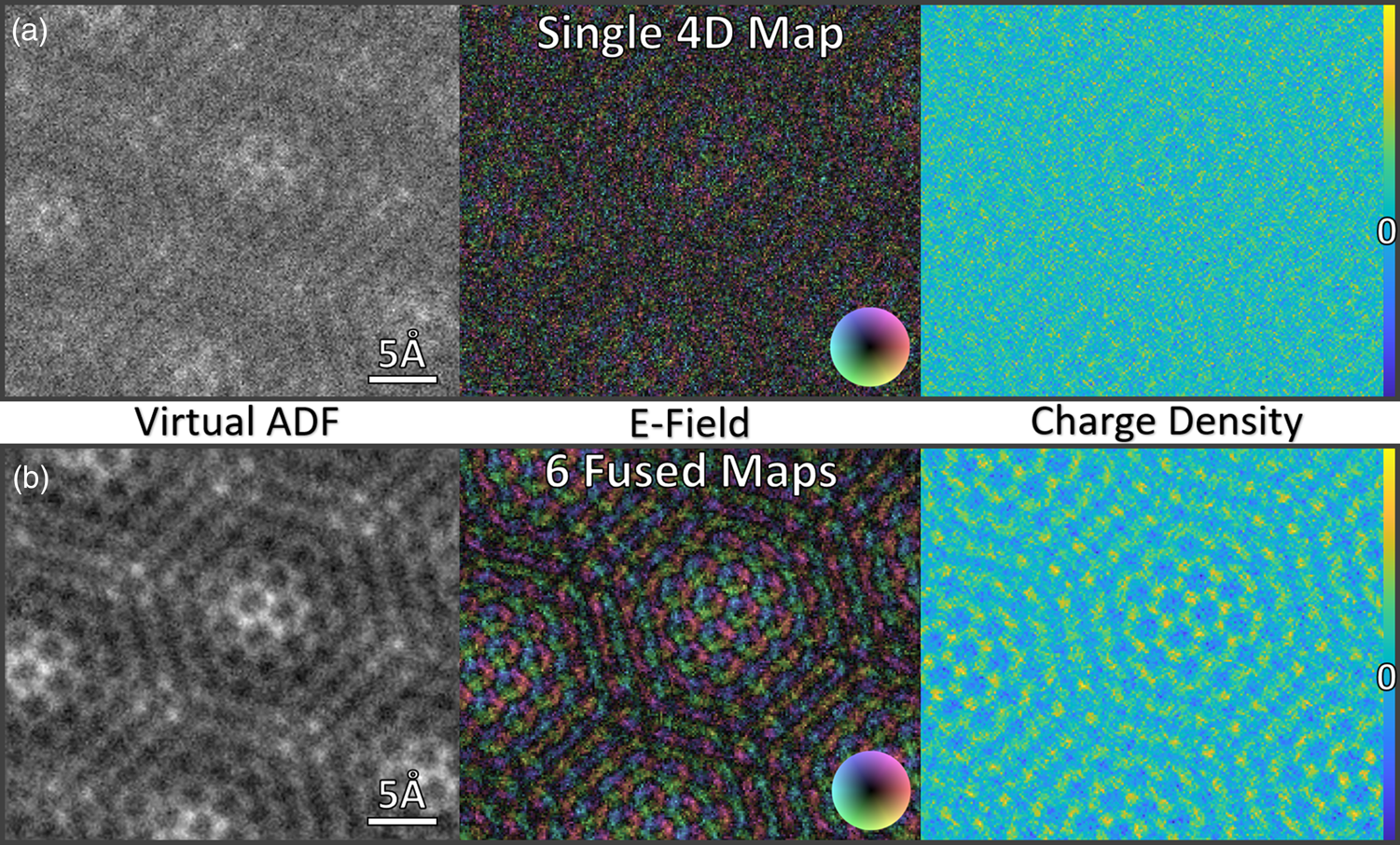
Fig. 6. Comparison of single 4D-STEM data set (a) and the sum of six fused (non-rigidly registered) maps (b) of a twisted bilayer graphene sample: virtual ADF image (left), E-field map (center), and charge-density distribution (right).
In summary, the dose-fusion allows one to obtain high-quality 4D-STEM data sets even for slow and noisy optically coupled detectors and, in the case of novel fast direct detectors, allows to harness their full speed and acquire multiple maps instead of having to increase the dwell time of a single map to boost the signal and thus introduce more artifacts from instabilities.
Increasing the number of frames of 4D data contributing to the sum increases the effective total electron dose used in each type of reconstruction, thus an increase in precision is expected.
The same is true of the electric-field map precision, where the curl operator of the field-map can be used to indicate the fidelity of the data. In this example, the curl was reduced from 0.0390 to 0.0173, an improvement of 2.25×. The COM analysis greatly benefits from correcting the probe positions due to the peculiar properties of the E-field signal on crossing atom positions.
Ptychography Analysis
To demonstrate the versatility of non-rigid registration of 4D-STEM data, we also compared the performance of non-iterative, single side-band electron ptychography reconstructions for individual and dose-summed registered data sets. The ADF images and phase reconstructions for both the single frame and dose-summed data are shown in Figure 7. Monolayer graphene is a weak-phase-object and thus provides poor dark-field signal in the detector plane as seen from the ADF in Figure 7a. A combination of registration and dose-summing is required to reveal the atomic columns with high spatial precision (Fig. 7b). The application of electron ptychography to single data sets as shown in Figure 7c can reconstruct phase maps with a much higher SNR than the simultaneously acquired ADF images. However, the fidelity of the reconstruction is hampered by the noticeable phase variations between identical atoms. By applying multi-frame acquisition, non-rigid registration methods and dose-summing before running the electron ptychography reconstruction, as shown in Figure 7d, the SNR, and hence the spatial precision of the phase reconstructions, can be improved significantly. The spatial frequency power spectra for these 4D data sets are shown in Supplementary Figure S2.

Fig. 7. Multi-frame ptychography of a graphene monolayer. (a) Typical single ADF frame (10 of 21) from the raw ADF series. (b) Aligned and non-rigid registered average ADF image cropped to 246 × 225 px. (c) Single side-band (SSB) phase image from an individual frame. (d) SSB phase image from the aligned and accumulated data set. Note: After alignment, cropping the common area present in all frames results in a small loss of image field-of-view.
To quantitatively demonstrate the improvement to SNR and phase precision for the ptychographic data, an integrated squared-phase cross-section (ISPCS) was evaluated for each atom in the phase reconstructions. The ISPCS is calculated by integrating the squared-phase values for a Voronoi cell around each atom. The reason that the squared-phase was chosen instead of the phase is as follows. The positive phase contributions from the atomic potentials are completely canceled out by the negative phase contributions from the surrounding vacuum. As such, the integrated phase over a Voronoi cell should equal zero. By squaring the phase, the signal from both the atomic potentials and surrounding vacuum is positive, resulting in a nonzero ISPCS value in each Voronoi cell. Figure 8 shows histograms of the ISPCS from a single 4D-frame (orange) and the dose-fused non-rigid registered ensemble (green).

Fig. 8. Histograms of the integrated squared-phase cross-section (ISPCS) for the central frame of the series (frame 10 of 21, orange) and for the non-rigid registered and summed data (Green). A normal distribution has been fitted to each histogram.
For a single frame, the ISPCS values for all the carbon atoms in the image have a standard deviation of 8.80 × 10⁻⁶ rad2 Å2. After dose fusion of 21 frames, the standard deviation for the same set of carbon atoms fell to 2.91 × 10⁻⁶ rad2 Å2. The standard deviation of the ISPCS was reduced by more than a factor of 3 with multi-frame acquisition and registration. This provides a significant improvement in feature interpretability as shown in Figure 7, which is particularly important for distinguishing subtle atomic number differences and bonding effects in light-element samples. It should be noted that the improvement in phase precision is less than the factor of √21 that would be expected from Poisson statistics for incoherent imaging methods. Ptychographic reconstructions do not follow Poisson statistics, and this might be the explanation for the slightly lower precision improvement. Although the mode of the two ISPCS values are similar, the mean can be seen to differ slightly. The single frame distribution is also somewhat asymmetric, which may be associated with the way scanning distortions affect the ptychographic reconstruction.
In addition to improving the phase precision, the increased SNR of registered and dose-summed 4D-STEM data can improve the contrast of high-resolution information in the phase reconstructions. This can be seen in the Fourier transform of the real-space phase maps as shown in Supplementary Figure S5. For the single 4D-STEM data set, the third order spots are the highest spatial-frequency observable indicating a resolution of 1.05 Å. After the distortion-correction and signal-fusion, the fourth order spots at 0.79 Å are clearly visible and the fifth order spots at 0.71 Å are marginally visible. This represents a resolution improvement of approximately 48%.
The 4D multi-frame alignment not only increases the dose available to the final reconstruction, but also increases the dose presented at the stage of the post-processing aberration diagnosis and correction procedures which can be performed as part of the ptychographic workflow (Yang et al., Reference Yang, Rutte, Jones, Simson, Sagawa, Ryll, Huth, Pennycook, Green, Soltau, Kondo, Davis and Nellist2016). Supplementary Figures S3 and S4 show example disk-overlap plots for a single-scan and the 21-frame dose-fusion volumes.
The first-order disk-overlaps (Supplementary Figs. S3 and S4, top row) corresponding to ≈4.8 nm−1 (or 0.65α) have an SNR that is ample for aberration diagnosis in both the single-frame and dose-fused data. The third-order overlaps however (Supplementary Figs. S3 and S4, bottom row), which correspond to ≈9.5 nm−1 (or 1.28α), show very little information in the single-frame but a significant improvement in SNR is seen after dose-accumulation and scan-distortion correction. After dose-fusion, the chromatic damping-envelope is even visible in the amplitude of the third-order overlaps (Supplementary Fig. S3, bottom-right), which can be utilized to reduce the chromatic defocus spread of ptychographic reconstructions (Nellist & Rodenburg, Reference Nellist and Rodenburg1994; Pennycook et al., Reference Pennycook, Lupini, Yang, Murfitt, Jones and Nellist2015). The improved SNR in the phase of the overlaps (Supplementary Fig. S4), especially at higher spatial frequencies, improves the performance of the aberration diagnosis and correction procedures which can be used along with ptychography to provide aberration-free phase reconstructions.
For both the COM and ptychography examples investigated, the improvements in electric-field self-consistency, phase precision, or spatial resolution, all depend on the precise scan-position errors and their interplay with the nuclear coordinates. A more expansive study is needed to determine the mathematical framework of what improvements should be expected with increasing numbers of frames.
Conclusion
In summary, it was demonstrated that the data fusion of nonrigidly registered 4D-STEM series enhances the SNR and improves the fidelity of scan positions without introducing artifacts. This enhanced “raw” data can then be processed like any other conventional 4D-STEM data set but with drastically enhanced results.
It was shown that the improved scan positions avoid phase corruption in the case of ptychography and greatly enhance the result of COM analysis, as the calculated E-fields strongly rely on the beam positions which are significantly imperfect in experimental 4D-STEM data sets. We observed a factor of 3 improvement in squared-phase precision, a 48% improvement in spatial resolution as well as improved robustness against cold-FEG emission instability.
As 4D-STEM data are severely noise-limited and this framework offers a way on how to extend the acquisition time and thus the dose and SNR without running into the typical problems associated with sequential data acquisition, it should be a way on how to reveal signals that are typically too weak to observe well, like the real-space observation of bonding influences. To facilitate this, it is ideal to combine this post-processing of 4D-STEM series with a simple (rigid) drift correction during acquisition, as not to lose the field of view during acquisition.
Although drift correction using reference frames has long been possible (Recnik et al., Reference Recnik, Möbus and Sturm2005), we have instead demonstrated an internal-reference approach based on series acquisition (Jones et al., Reference Jones, Yang, Pennycook, Marshall, Van Aert, Browning, Castell and Nellist2015).
While ptychographic and center-of-mass type data sets have been the focus of this manuscript, all the methods described are nevertheless applicable to other multi-frame 4D measurements such as STEM diffractive imaging, STEM symmetry imaging (Krajnak & Etheridge, Reference Krajnak and Etheridge2020), or magnetic field imaging (Krajnak et al., Reference Krajnak, McGrouther, Maneuski, O'Shea and McVitie2016; Paterson et al., Reference Paterson, Webster, Ross, Paton, MacGregor, McGrouther, MacLaren and Nord2020). Our approach is not limited to high-resolution data; this was chosen as an especially challenging example, but other 4D-STEM scenarios like scanning nano-beam maps can be treated in the same way.
Supplementary Material
To view supplementary material for this article, please visit https://doi.org/10.1017/S1431927621012587.
Acknowledgments
The authors acknowledge the use of characterization facilities within the David Cockayne Centre for Electron Microscopy, Department of Materials, University of Oxford and in particular the EPSRC (EP/K040375/1 “South of England Analytical Electron Microscope”) and additional instrument provision from the Henry Royce Institute (Grant reference EP/R010145/1). L.J. acknowledges SFI grants URF/RI/191637 and AMBER2-12/RC/2278_P2. B.H. and C.T.K. gratefully acknowledge the German Science Foundation (DFG) funding in the form of the “BerlinEM Network” project (KO 2911/12-1) and the SFB951 HIOS (Projektnummer 182087777). The authors thank Alisa Ukhanova (Lomonosov Moskau State University) and Oleg Busanov (Fomos-Materials) for providing and preparing the GAGG sample, Xiaomin Xu & Norbert Koch (Humboldt-Universität zu Berlin) for the WS2 sample and Andreas Mittelberger (Nion Co.) for providing a 4D-STEM plugin for the Nion Swift software.


 Open access