


Introduction
Computed tomography (CT) has been commonly used in medicine for assessing the anatomy of humans in conventional computer axial tomography (CAT) scans. It is also a very common tool for assessing the architecture of trabecular bones for diagnosis of conditions such as osteoporosis [Reference Wang, Masse, Leng, Hess, Ross, Roeder and Niebur1]. More recently, high-resolution CT (micro-CT) has found increasing use in materials science for the evaluation of the internal structure of a variety of advanced materials for industrial applications. Knowledge of the micro-architecture of these materials is extremely important to better understand their performance. Micro-CT is a non-destructive 3D characterization tool that uses X rays to determine the internal structure of objects through imaging of different densities within the scanned object. High-resolution laboratory-based micro-CT or nano-CT provides image resolution on the order of 300 nm [Reference Withers2] [Reference Kastner, Harrer, Requena and Brunke3]. Such high resolution allows one to visualize the internal 3D structure of fine-scale features. The data from micro-CT results in a virtual rendering of the object under investigation, which allows one to travel through the volume in any direction and angle, revealing complex hidden structures within the object. Thus, micro-CT can be an important complementary technique for a microscopy laboratory.
Micro-CT can serve as a useful tool to screen materials for defects such as cracks, delaminations, and voids from the initial phase of product development to quality control of final part fabrication [Reference van Kaick and Delorme4] [Reference Brunke, Neuber, Lehmann, Lin, Ryan, Wu and Yoon5]. It is also widely used in metrology for inspecting components made with additive manufacturing techniques, reverse engineering, and computer-aided design (CAD) modeling [Reference Suppes and Neuser6]. The total scan time is relatively short, depending on the shape and size of the object. Also, compared to other microscopy techniques, the sample preparation required for micro-CT imaging is minimal.
The Instrument
This article describes the capabilities of the v|tome|x m CT, developed by GE Sensing & Inspection Technologies GmbH, Wunstorf, Germany. This instrument comes with dual X-ray tubes: (1) a unipolar, high-power micro-focus tube with a reflection target that can go up to a maximum of 300 kVp at 500 W and (2) a nanofocus X-ray tube with a transmission target that can go up to a maximum of 180 kVp at 15 W. Images of the instrument interior are shown in Figure 1. Imaging is accomplished with a cone beam, providing a geometric magnification at the detector. Magnification is determined by the ratio of the sample-to-detector distance to the sample-to-source distance. The minimum achievable pixel size for the microfocus tube is about 2 μm, and that for the nanofocus tube is below 1 μm [7]. Here, pixel size is purely determined by geometry. The spatial resolution of the image also depends on pixel blurring by the imaging apparatus, prenumbral blurring due to the source size, imaging conditions, and reconstruction. The unique high-power microfocus tube can detect details less than 1 micrometer in size, providing imaging of highly absorbing industrially relevant samples. The nanofocus tube can be used for low-absorbing materials, producing high-resolution images exhibiting detail less than 500 nm wide. Here detail detectability is the smallest size of an object that can still be seen in an image, even though it is smaller than the voxel size. This is particularly high for features with high contrast with respect to the bulk sample.
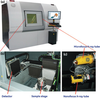
Figure 1: (a) Photo of the GE v|tome|x m. Insets (b) and (c) show the inside of the instrument. The two X-ray tubes, sample positioning stage, and detector are indicated.
Both X-ray tubes are open-type: they use a tungsten filament to generate electrons, which produce X rays from a tungsten target. The nanofocus tube has a transmission target sputtered onto a diamond window, which permits a considerably smaller focus spot size, distributes heat more efficiently, and allows higher power on a smaller focal spot. The smallest focal spot size for the nanofocus tube is about 3 μm, and that for the microfocus tube is about 7 μm. This allows high resolution images to be collected quickly. The cooling system for the X-ray tubes provides high beam stability at high power and small beam sizes. X rays are detected by a temperature-stabilized digital GE DXR250RT detector, with a one-megapixel array (1,000 × 1,000 pixels), where the pixels are each 200 μm square. The fast frame rate and read-out time of the detector (30 frames per second) shows “live” images of the sample in the field of view (FOV) during set-up, allowing easy sample alignment. The detector instrumentation may be translated laterally so as to double the width of the FOV and accommodate off-centered or odd-geometry samples.
The instrument has a robust sample chamber with granite-based four-axis sample positioning, an air-bearing rotation stage, and a translation resolution of 1μm (Figure 1b). Figure 2 shows a linear relationship between the sample-to-focal spot distance (which can be considered the largest possible diameter of the sample) as a function of the voxel size achieved. The largest diameter and height of the object that can be imaged is 300 mm × 400 mm (for both the microfocus and nanofocus tubes). Further, the tube power (accelerating voltage × filament current) for any image acquisition is limited by the voxel size, because both the micro- and nano-focus tubes have a focal spot size that dynamically increases with power. A focal spot size larger than the voxel size results in blurring of the pixels in the CT image. Therefore, for higher-density objects, lower resolution may be seen if the applied potential is increased to achieve greater power for penetration.
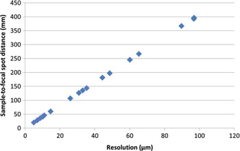
Figure 2: Graph of the sample-to-focal spot distance vs. resolution for the microfocus and nanofocus tubes in the V|tome|x M CT scanner.
Image Acquisition and Analysis
An X-ray radiograph image is essentially a map of the linear attenuation coefficient of every point in the sample. X-ray attenuation (μ) follows an exponential relationship with the incoming and outgoing X-rays from the sample as shown below [Reference Hubbell and Seltzer8]:
 $$
d_{{\rm total}} = {{\sqrt {r_D^2 + \left( {S{{r_{od} } \over {r_{so} }}} \right)^2 } } \over M}
$$
$$
d_{{\rm total}} = {{\sqrt {r_D^2 + \left( {S{{r_{od} } \over {r_{so} }}} \right)^2 } } \over M}
$$where I o is the intensity of the incoming X-ray beam, I is the intensity of the outgoing beam, and ρ is the density of the material comprising the sample. Filtered back-projection algorithms are used to reconstruct the 3D image volume from the acquired 2D data sets. Gray levels in a reconstructed CT image represent attenuation in each pixel. Therefore, a higher-density phase appears brighter (similar to X-ray film analysis) and is distinguishable from a lower-density material.
In general, the microfocus tube is used for imaging highly absorbing samples, and the nanofocus tube is used for lighter materials. For high-resolution micro-CT (<10 μm voxel size), the nanofocus tube is used, because it has a smaller focal spot size than the microfocus tube at the same tube voltage and filament current. If greater signal is required through a sample, but the tube power cannot be increased further due to limitation on the focal spot size, the exposure time of the image can be adjusted, with values ranging from 33 milliseconds to 5 seconds. Further, the signal-to-noise ratio can be increased by averaging more frames per image. The parameters used for imaging the objects described in this article are listed in Table 1.
Table 1: Table showing the imaging parameters for all the examples discussed in this article. The target material for all the specimens is Tungsten.

The X rays generated from a laboratory X-ray instrument are usually polychromatic. The characteristic lines of the target material (Tungsten in this case, K-edge at 69.5 keV) are super-imposed over the Bremsstrahlung radiation. Low-energy photons are easily absorbed by the sample without contributing much to image formation. This phenomenon is the reason for the beam-hardening artifact [Reference Barrett and Keat9]. Beam hardening occurs when the mean energy of the X ray increases as they pass through the object because of the higher absorption of lower-energy photons. As the beam becomes harder, the rate at which it is attenuated decreases, so the beam received by the detector is more intense than would be expected if it had not been hardened. X rays passing through the middle portion of a uniform cylindrical specimen are hardened more than those passing through the edges because they pass through more material. Thus the central portion of the sample appears darker. This effect can be mitigated by pre-filtering the beam with thin sheets of metal, placed outside the exit window of the X-ray tube. Filters are usually chosen such that they remove the lower-energy photons of a spectrum. The application of these added filters requires an increase in the exposure factors (voltage, current, and exposure time) to compensate for decreased X-ray flux.
Another common artifact arises when the sample partially swings in and out of the FOV of the detector at certain rotation positions. This appears as a bright ring in the reconstructed volume at the boundary of the FOV; this artifact can be subtracted mathematically during reconstruction. Artifacts can also arise in an image because of defects in the detector. One such artifact is the ring artifact, which appears as circular rings in the reconstructed volume, emanating from the center of rotation of the sample. This artifact arises because of non-linearity in the response of the pixels in the detector. The detector in the v|tome|x M has a built-in capability that shifts the detector by a few pixels randomly during image acquisition to minimize this effect.
The quality of images can be further improved or adjusted during image reconstruction by the application of mathematical filters. The median filter is commonly used for reduction of noise in the image. The Phoenix X-ray commercial software, Datos|x, also has pre-calibrated beam-hardening-correction and ring-artifact-reduction filters with various kernel sizes. These filters have to be used with caution so as to not artificially reduce the resolution of the image.
The reconstructed volumes are typically exported in 32-bit format and read into Volume Graphics Studio MAX 2.1 [10]. This format has great bit-depth for image manipulation and segmentation. However, for optimizing the size of the volume file, a 16-bit format volume can also be used. For analysis with the 2D image analysis software, Clemex Vision PE [11], a stack of images is exported in .tiff format.
Results
Example 1: Porosity in carbon-epoxy composite. Figure 3a–3c shows three orthogonal views of a carbon-epoxy composite. The bright regions are bands or bundles of continuous carbon fibers (defined as a tow) surrounded by darker regions, identified as the matrix or resin material. The voids in the sample are clearly seen as the darkest regions in the image. The imaged sample is a rectangular block with dimensions 25.4 mm (1″) height, 12.7 mm (0.5″) width and 3.2 mm (0.125″) thick. The imaging parameters are summarized in Table 1. Figure 3a shows multiple layers of tows because the CT slice did not evenly slice through a single layer of tows. The dark voids are mostly located at the interfaces between tows in the composite. Moreover greater porosity is present in the top half of Figure 3b and right half of Figure 3c.

Figure 3: (a)–(c) Single CT slices of the three orthogonal views of carbon-epoxy composite. The orientation of the image planes (a)–(c) in the sample are indicated by green, blue, and red planes, respectively, in (d). The width of the images (a) and (b) to scale is 11.4 mm, and that of (c) is 2.5 mm.
The imaged volume was analyzed for porosity using the Defect Detection module in VG StudioMAX [10]. The porosity values determined here serve as feedback in the material development process. The region of interest (ROI) was segmented using specific values identifying the voids in the material. The module then uses specialized algorithms to find voids within the range of gray values specified by the user. The volume size distribution of pores was calculated, and the results are shown in Figure 4. From these data the porosity was calculated to be 1.6%. The largest pores have an average diameter of 554 μm, and the average diameter of all the pores in the sample is 136 μm.
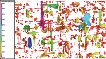
Figure 4: Image of the volume size distribution of pores in a carbon-epoxy composite. The width of the image to scale is 13.8 mm.
The same volume was also analyzed for porosity using Clemex Vision PE [11]. The pore area was calculated for each CT slice along the 8.3 mm (0.325″) dimension. Figure 5 shows the pore area fraction as a function of depth in the sample. As suggested from the CT slices shown in Figures 2b and 2c, the porosity increased from one side of the sample to the other. The mean porosity value for all the 2D slices was 1.4 ± 0.7%. This value compares well with the porosity of 1.6% determined from direct volume analysis and thus helped confirm the validity of the porosity determination technique.
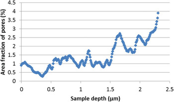
Figure 5: Plot of area fraction of pores in a carbon-epoxy composite as a function of CT slices through the depth of the sample.
Example 2: Carbon-epoxy composite architecture.Figure 6 shows an example of a carbon-epoxy composite test part for an aerospace application. As can be seen from the overall view of the test piece in Figure 6a, generated from a volume rendering of CT slices, the geometry of the part is fairly complex. However, the advantage of using CT here is that parts of any shape can be imaged with minimal sample preparation.
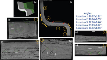
Figure 6: (a) Overall 3D view of carbon-epoxy composite test part. (b) CT slice of the test piece for one orthogonal view indicated by the green plane in (a). The width of (b) is 31.7 mm, to scale. The solid yellow lines indicate the orientation of the CT slices going into the plane, with respect to the sample geometry. (c)–(g) show the different locations (1–5 indicated in Figure 5b) where the angle between the 45° plies was measured.
Figure 6b shows a cross section of the sample along the green plane indicated in Figure 6a. Figure 6b shows that the test part is made up of 16 layers of tows. The detailed architecture of the fiber tows can be seen in Figures 6c, 6e, and 6g, showing axial and ±45° tows in the imaging plane. For the image plane in Figure 6b, the 45° tows come out of the plane, and thus the gaps between two adjacent 45° tows are seen in cross section as small, nearly circular voids, indicated by red arrows. The ability of CT to slice the sample in any direction and at any angle proves very advantageous here, because it allows the part to be inspected in a plane tangential to the curved sections. The measured angles between the +45° and −45° plies are shown for sections at locations 1–5 shown in Figure 6b. Figures 6c–6g show examples of these angle measurements, which range from 90.1 ± 1.2° at the base of the sample, to 94.3 ± 0.9° at its top. This variation suggests that as the plies are formed to their final shape, the resin allows sliding between and within them, as explored for draping [Reference Neoh12]. Incomplete consolidation of the plies is evident at location 4 in Figure 6b. This can also be seen in other cross sections shown in Figures 6e (near the bottom) and 6g (near the top) as gaps between the layers. Such information is valuable for optimizing the temperature and pressure conditions for consolidation of the plies in the composite.
Example 3: Electronic component failure analysis. Micro-computed tomography also serves as a tool for detection of electronic component failures or to rapidly pre-screen defective parts for quality control in manufacturing, without actually cutting them apart [Reference Roth13]. This has gained increasing importance because of the rapid advancement of the microelectronics industry, which requires stringent reliability and cost-effective defect testing. Figure 7 shows a tomographic slice from part of an NVidia Graphics processor, where a ball grid array attaches a microelectronic component to a circuit board. The solder is easy to identify because it is made up of a high-density material. Each solder ball is about 500 μm in diameter. This image was acquired by placing the entire board with dimensions ~101.6 mm (4″) × 152.4 mm (6″) in the X-ray FOV. Figure 7a is from a failed circuit board, and Figure 7b is from a new circuit board. The failed board is damaged near the top-left corner, where the solder balls are fused. The defect might have occurred at the micro-joints because of thermal stress from a mismatch in the coefficient of thermal expansion between the circuit board and the solder or from mechanical stress due to vibration and flexing.
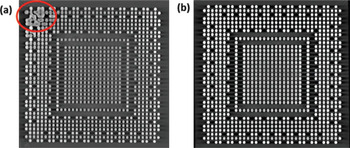
Figure 7: Shows an array of solder balls from (a) a damaged microelectronics circuit board and (b) a new circuit board. The widths of the images (a) and (b) respectively, to scale, are 30.7 and 31.2 mm.
Example 4: Non-destructive identification of cracks in a Ni-base superalloy. The following example is of a fractured cylindrical bar of a single-crystal Ni-base superalloy for gas turbine blade applications [Reference Tin14]. The cylindrical specimen with a gage diameter of 5 mm was subjected to fatigue testing at elevated temperature until failure. The mean stress was positive at the end of the fatigue test. The goal of this CT inspection was to determine the size, shape, and distribution of cracks within the gage section of the sample. This CT inspection is the first of its kind; it uses the high-power and high-resolution capability of the instrument. To the authors' knowledge, samples of this size and material have not been inspected using CT at this resolution. The imaging parameters for this example are listed in Table 1.
Figures 8a, 8c, and 8d show CT slices of the sample for three orthogonal views. Figure 8b shows the 3D location of the image plane in Figure 8a. The beam-hardening artifact is clearly visible as a brighter outer edge in this specimen. Filters were not applied to remove this artifact during reconstruction of the volume so as to preserve the details in the images. The crack shown in Figures 8a, 8c, and 8d is one of the largest cracks found in the sample.
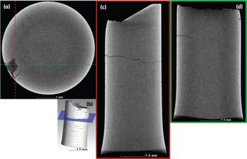
Figure 8: (a) Transverse cross section of a cylindrical tensile specimen of a Ni-based superalloy at the location of the deepest crack. The width of the figure is 5.2 mm. (b) The blue plane indicates the location of the cross-sectional slice in (a). (c)–(d) show longitudinal cross-section images along planes indicated by the dashed red and green lines respectively in (a). The width of (c) and (d) are 4.7 mm and 5.7 mm respectively.
As seen in Figure 8a, the crack extends from the bright region to the dark region of the sample. A common intensity threshold could not be determined for these kinds of cracks and thus required manual segmentation. Therefore only a selected few cracks have been segmented in the volume rendering of the scanned object shown in Figures 9a–9b. The crack has a typical thumbnail shape. All the cracks detected have propagated in a direction perpendicular to the applied axial tensile stress. In addition to the selected cracks, a large number of circumferential surface cracks are present in the sample as seen in the volume rendering of Figure 9b.

Figure 9: (a) Volume rendering of the sample of Figure 8 reconstructed from CT slices. The segmented cracks are colored red. (b) The sample is made semi-transparent to show the segmented cracks more clearly.
Discussion
Large and odd-shaped geometry samples are common in an industrial setting. The double-width feature of the detector and multiple-scan capability of the sample stage and software in the GE v|tome|x M accommodate this for most cases. However this increases the total imaging time, especially for the case of thick or very dense samples (which will require long exposure times for each image). In many cases, multiple samples of the same kind require sequential processing. If there were a way to eliminate operator interaction for each individual sample by using a sample robot in these laboratory-based systems, the throughput could be increased significantly. Most synchrotron-source-based CT systems have an advantage in this respect [Reference Mayo, Stevenson and Wilkins15, Reference De Carlo, Xiao and Tieman16, Reference Mader, Marone, Hintermuller, Mikuljan, Isenegger and Stampanoni17].
Several differences exist between the X rays produced by laboratory and synchrotron sources [Reference Brunke, Brockdorf, Drews, Müller, Donath, Herzen and Beckmann18]. Although the resolution achieved by lab X-ray sources is similar to that obtained by synchrotron sources, the synchrotrons have the advantage of having higher flux, resulting in much shorter acquisition times (full tomographic data sets are acquired in 5–10 minutes at several sources [Reference Mader, Marone, Hintermuller, Mikuljan, Isenegger and Stampanoni17]), as well as the ability to tune the wavelength of the X-ray beam. However, the trade-off is a much smaller FOV and the requirement of a smaller sample size. The resolution provided by state-of-the-art laboratory CT systems is improving due to recent developments in cooling technology of the detector and X-ray tubes with rotating targets, high beam stability, long-life filaments, and advanced optics for smaller focus spot sizes and cone beams. The dual-tube technology for the v|tome|x m offers enhanced flexibility with respect to the kinds of samples that can be investigated and eliminates the need for two separate instruments.
Another common limitation to high throughput is CT image analysis [Reference Buie, Campbell, Klinck, MacNeil and Boyd19, Reference Malcolm, Leong, Spowage and Shacklock20]. As seen in Example 4, the presence of artifacts requires greater user interaction with the imaging software. Although the results might be very precise, the total time required increases. However, with rapid advancement in software capability and computing power, manual intervention in the future should be minimized.
Conclusion
This article shows several examples of applications of a micro-computed tomography (micro-CT) tool for materials characterization. State-of-the-art laboratory-based CT systems now have ⟨1 μm detail detectability and can examine large samples. These systems can be used for qualitative detection of cracks and voids, as well as quantitative analysis of porosity, crack measurements, and metrology.
Acknowledgments
The authors would like to thank Mark Vermilyea, Xiaomei Fang, David Shaddock, Bernard Bewlay, Akane Suzuki, and Mallik Karadge at the GE Global Research Center (GE GRC) for providing us samples to work with and several useful discussions. We would also like to thank Oliver Brunke and Dirk Neuber at GE Measurement & Control, Inspection Technologies for help with the preparation of the manuscript.


