


Introduction
Terahertz non-destructive testing (NDT) applications have recently found their way into industrial contexts, where specific problems of defect detection and quality inspection can be addressed. Terahertz radiation is commonly defined to cover the frequency range from 0.1 up to 10 THz corresponding to electromagnetic waves with wavelengths of 3 mm down to 30μm. In many cases, this range of wavelengths matches typical dimensions of relevant structural features or defect sizes in workpieces of modern production processes. Since terahertz radiation penetrates most non- or weak conducting materials, a volumetric inspection of raw monolithic materials but also multi-layered composite materials [Reference Friederich, May, Baccouche, Matheis, Bauer, Jonuscheit, Moor, Denman, Bramble and Savage1] and entire assembled components is possible [Reference Naftaly, Vieweg and Deninger2–Reference Herschel and Pawliczek6]. Due to low energy levels and commonly relatively low generated radiation powers, terahertz technologies are non-hazardous and safe to be used by human operators, and, because of their electromagnetic nature, can work contact-free. Terahertz inspection systems for NDT purposes may be applied in very early stages of production processes [Reference Ellrich, Bauer, Schreiner, Keil, Pfeiffer, Klier, Weber, Jonuscheit, Friederich and Molter7, Reference Bauer, Hussung, Matheis, Reichert, Weichenberger, Beck, Matuschczyk, Jonuscheit and Friederich8] but also for tasks of supervision in recurring maintenance cycles [Reference Bauer, Matheis, Mashkin, Krane, Pohlmann and Friederich9]. A typical application scenario of the latter is the formation of internal defects – such as cracks, delaminations, water inclusions, etc. – in products under heavy workload over an extended period of time. Terahertz technologies can provide a complementary approach to established NDT techniques, such as x-ray, ultrasound, radiography, and others. In some cases, the unique properties of terahertz waves can even help to address very specific problems of quality control, where other technologies may not be applied.
One class of terahertz measurement systems employs all-electronic terahertz sources, detectors and receivers, and are therefore often referred to as electronic terahertz systems. Such system usually work in continuous-wave (CW) mode at single defined frequencies as opposed to pulsed terahertz system, where the generation of the radiation is commonly based on ultrashort laser pulses. Nevertheless, electronic CW terahertz systems may provide some range of frequency tunability around a given center frequency. With the so-called frequency-modulated continuous wave (FMCW) measurement technique, a linear modulation of CW terahertz radiation is used to provide distance information in terahertz measurements of (terahertz-transparent) objects under test.
Typically, terahertz inspection is combined with various imaging techniques[Reference Valušis, Lisauskas, Yuan, Knap and Roskos10–Reference Ding, Kahl, Loffeld and Bolívar12], in order to yield 2D cross-sectional images of individual layers and/or full 3D volumetric data of objects under test. According to the applied wavelengths, the image resolution is usually on a millimeter to sub-millimeter scale. A common approach in the generation of terahertz images is the use of quasi-optical beam-forming elements such as lenses and mirrors. In many scenarios, a terahertz point source is collimated by a first lens – typically made of materials of relatively low refractive index such as PTFE or HDPE – or an off-axis paraboloidal mirror (OAP) and then focused onto a target by a second focusing lens or OAP. The focal lengths of the quasi-optical elements can be varied to some degree regarding the specific application scenario, but larger focal length leads to reduced image resolutions and fields of view. On the other hand, the focal lengths cannot be reduced below a certain practical minimum, which leads to a restriction in minimum working distance from the terahertz source to the objects to be measured.
Here we present our recent approach to combine low-dielectric waveguide antennas with FMCW terahertz transceivers to overcome some of the above limitations, in particular the application of terahertz measurements in an environment with very limited access space to perform NDT imaging. The development of the measurement system presented in this contribution was driven by a highly relevant NDT scenario, namely the in-situ inspection of the insulation of stator bars of power plant generators.
Motivation
Figure 1(a) shows the end winding region of a turbogenerator consisting of a larger number of individual generator bars forming the generator's stator. The bars can be recognized in the photo by the red color of an insulation tape wrapped around them. The yellow stripes are epoxy-impregnated bands which tie adjacent bars to each other and hold them in place. Below, a photograph shows the cross-section of a single generator bar. The center region consists of copper strands forming the actual conductor, which is surrounded by an insulation made of mica material. The structural integrity of these mica layers is crucial to prevent high-voltage breakdowns of the insulation. However, close to the regions where the bars bend outwards, cracks in the mica insulation can form due to the very high thermomechanical stress the turbogenerators undergo during operation. Usually, such cracks start to form inside the insulation but below the surface and are invisible from the outside. Hence, the damages can only be found in conventional, visual inspections once they extend through the whole insulation up to the surface after some time. At this point, the bars have to be cut out from the generator, resulting in significant downtimes of the power plant.
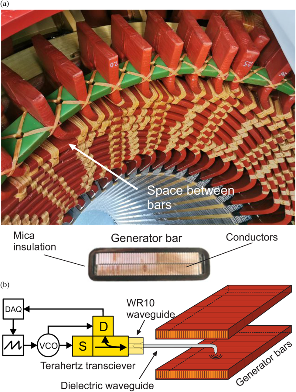
Fig. 1. (a) End winding region of a stator from a turbogenerator. The bending regions of the generator bars are prone to developing sub-surface cracks in the mica insulation under thermomechanical stress. The photograph at the bottom shows the cross-section of a bar with center conductor and surrounding insulation. (b) Schematic illustration of the terahertz FMCW measurement system (see section “FMCW principle”) with dielectric waveguide antenna for non-destructive testing of the mica insulation in the limited access space between adjacent bars.
Terahertz FMCW imaging of the generator bar's insulation can provide a solution to this problem and help to detect the formation of sub-surface cracks already at an early stage, where a repair of the mica insulation is still possible. Ideally, the terahertz NDT inspection can be performed during regular maintenance intervals on site at the power plant without the need to dismantle the generator and pull the rotor. The main challenge of this specific task, however, is the very limited access space of less than 20 mm between adjacent bars, which prevents the use of a classical quasi-optical system design for terahertz imaging. We therefore integrated in our measurement system a dielectric waveguide antenna designed in such a way that it can reach inside the space between the generator bars.
Technological approach
Dielectric waveguide structures have long been known to provide a feasible way to guide electromagnetic radiation in a confined way and with sometimes greater flexibility compared to free-space propagation. In general, the aim is to provide strong guidance of the terahertz waves and at the same time keep radiative losses at an acceptable level. Various approaches exist [Reference Yeh and Shimabukuro13–Reference Humbert15], where the specific implementation of dielectric waveguides may, for example, be realized in the sense of hollow-core and porous-core fibers [Reference Pan, Chopard, Fauquet, Mounaix and Guillet16, Reference Koala, Fujita and Nagatsuma17] or as solid dielectric materials, sometimes referred to as ribbons or dielectric rod waveguides or microwires [Reference Koala, Fujita and Nagatsuma17–Reference Baccouche, Baktash, Clemens, Natale, Jonuscheit and Friederich24] exploiting total internal reflection. Even the combination of dielectric rods with embedded substrate lenses has recently been investigated for integration with antenna emitters [Reference Rivera-Lavado, García-Muñoz, Lioubtchenko, Preu, Abdalmalak, Santamaráa-Botello, Segovia-Vargas and Räisänen25]. Solid dielectric waveguides can be fabricated from both high or low dielectric constant materials, which has some direct impact on the efficient coupling geometry to hollow waveguide structures [Reference Yeh and Shimabukuro13]. Recently, solid dielectric waveguides made from low-loss dielectric semiconductor materials such as high-resistivity silicon, sapphire, or GaAs [Reference Räisänen, Generalov, Lioubtchenko, Rivera-Lavado, Méndez-Aller, García-Muñoz, Segovia-Vargas and Preu26] have gained some interest, in particular for planar and hollow waveguide integration [Reference Koala, Fujita and Nagatsuma17]. For our implementation, however, we choose a solid dielectric waveguide of low dielectric constant material, e.g., polyethylene (PE) [Reference Weinzierl, Fluhrer and Brand20, Reference Weinzierl, Richter, Rehm and Brand21], mainly due to ease of fabrication and specific challenges for the task described above. For our employed frequencies in the W-Band we do not expect significant signal degradation due to power losses in the plastics material [Reference Jin, Kim and Jeon27] (see section “Dielectric waveguide antenna”)
Figure 1(b) illustrates our specific measurement scenario, where a dielectric waveguide antenna with 90 degree bend at the end is attached to an all-electronic, waveguide components-based terahertz FMCW transceiver. By appropriate design of the dielectric waveguide antenna we achieve a perpendicular incidence of the terahertz radiation in a near-field-like setup. In combination with an appropriate scanning mechanic (see section “Conclusion and outlook”), a raster scan image of the bar's insulation, with limited access space between generator bars, can be recorded on site at the power plant without the need to cut out parts of the generator bars for later inspection.
In this paper, we present our system approach for this specific measurement scenario at hand. We discuss system design and performance evaluation and show some first measurement results of model samples and also real generator bars with real-world defects. We also give an outlook on ongoing tasks, mainly regarding automation of the measurement process and further optimization of the dielectric waveguide antennas in terms of waveguide coupling and power losses. Note that some of this work was already presented in an earlier version of this paper at the 51st European Microwave Conference EuMC, London 2021, and was published in its proceedings [Reference Bauer, Matheis, Mashkin, Krane, Pohlmann and Friederich9].
Terahertz FMCW measurement system with dielectric waveguide antenna
Terahertz imaging systems often rely on beam-forming optics such as quasi-optical systems offering some degree of flexibility in terms of the selection of focal lengths and thus working distance. On the other hand, quasi-optical components for the terahertz range are usually quite large and proper alignment for diffraction-limited terahertz imaging, especially in the lower terahertz frequency region, can be difficult. One alternative is dielectric waveguides as near-field antennas for all-electronic terahertz imaging, where due to the relatively small bandwidths, dispersion inside the dielectric materials is of minor concern. Dielectric waveguide antennas can be realized in various forms and offer sub-wavelength imaging resolution in combination with relatively simple manufacturing methods and versatile design freedom, depending on the dielectric material. The antennas can be easily integrated into typical waveguide horns of electronic terahertz systems to ensure efficient power coupling to the dielectric [Reference Yeh and Shimabukuro13, Reference Pan, Chopard, Fauquet, Mounaix and Guillet16, Reference Yeh, Shimabukuro and Siegel19–Reference Weinzierl, Richter, Rehm and Brand21].
We present here a combination of the concept of dielectric waveguide antennas with an all-electronic FMCW terahertz transceiver for NDT imaging in limited access spaces, where conventional, quasi-optical terahertz systems are too large. We will first introduce the FMCW concept and then discuss the implementation of our dielectric waveguide antenna. It should be mentioned at this point that recently, the use of a hollow dielectric waveguide antenna in combination with a comparable terahertz transceiver unit was presented in the literature [Reference Pan, Chopard, Fauquet, Mounaix and Guillet16]. Although a slightly different approach was employed there, the reader may find some of the theoretical considerations and simulations on forward power coupling and beam profiles useful for further insight.
FMCW principle
We employ an all-electronic terahertz FMCW transceiver architecture as illustrated in Fig. 1(b). Note that all HF electronics and waveguide components are mounted in a single FMCW transceiver unit as shown in the drawing in Fig. 12. The principle of terahertz generation in electronic sources relies on frequency multiplication of conventional HF frequencies into the terahertz range by diode-based, waveguide-integrated frequency multipliers. For the generation of the linear terahertz frequency modulation, analog output voltage ramps are generated by a commercially available data acquisition unit (DAQ). The voltage ramps are then converted into linear frequency ramps (here: from 12 to 18 GHz) by a voltage-controlled oscillator (VCO). These linear ramps are then fed to an active multiplier chain (S) upconverting the frequencies into the W-Band. In the particular setup presented here, we address a target frequency bandwidth of 40 GHz from 70 to 110 GHz. For the NDT measurements, the FMCW terahertz radiation is sent through a waveguide directional coupler with attached waveguide horn antenna. Instead of using the free-space radiation, here we couple into our dielectric waveguide antenna for guidance of the radiation into the space between generator bars. The terahertz waves are emitted at the tip of the bent dielectric waveguide forming a quasi-point source for near-field like imaging. The same dielectric antenna receives the terahertz signals reflected from a target under test. The received radiation is mixed with the original reference signal in a Schottky diode-based receiver (D) and down-converted into an IF band at MHz frequencies. A fast DAQ is used for direct sampling of these resulting difference frequencies.
Since the emitted and received terahertz frequency ramps are shifted due to the finite travel time to the target and back, Fourier-transforming of the recorded IF frequencies yields a time-of-flight or distance information of the measured signals. Figure 2 illustrates the FMCW measurement principle (for some further details on the FMCW transceiver, see, e.g., [Reference Ellrich, Bauer, Schreiner, Keil, Pfeiffer, Klier, Weber, Jonuscheit, Friederich and Molter7]). The terahertz waves can also penetrate the target through layers of non-conducting materials, and individual reflections at material interfaces will result in separate IF frequencies in the receiver system. For each recorded reflection at IF frequency f IF, the distance d(f IF) to the measurement system can be calculated as

with c 0 the vacuum speed of light, n the effective refractive index of the material, ΔT the sweep time, and Δf the sweep bandwidth of the linear frequency ramps. The temporal quantity τ(f IF) represents the traveling time of the respective terahertz signal to the target and back to the transceiver. The achievable depth resolution in FMCW reflection radar is related to the sweep bandwidth as Δr = c 0/2nΔf and amounts to approximately 4 mm for the employed terahertz transceiver [Reference Ellrich, Bauer, Schreiner, Keil, Pfeiffer, Klier, Weber, Jonuscheit, Friederich and Molter7]. With the FMCW measurement technique, single-point depth profiles (sometimes referred to as A-scans) are obtained. When combined with an appropriate scanning mechanics, quasi-3D volumetric images of an object can be recorded.
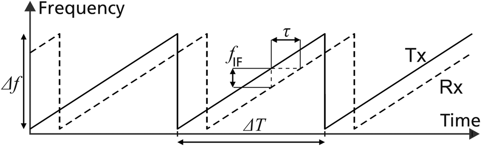
Fig. 2. Illustration of the FMCW principle to obtain distance information from CW measurements.
Dielectric waveguide antenna
Our terahertz system is equipped with a dielectric antenna made of PE material for non-contact, near-field imaging. An additional 90 degree bend at the end of the waveguide allows application in a very limited space of less than 20 mm height, as in the intermediate space between power generator bars (see Fig. 1). The dielectric waveguide antenna is shown in Fig. 3, where an additional, 3D-printed hollow ABS (acrylonitrile butadiene styrene) sleeve is attached to mechanically stabilize the antenna close to both ends with small pieces of polystyrene foam (we find no significant influence of the sleeve on system performance in comparative measurements, data not shown here). The antenna has a total length of 140 mm outside the waveguide flange and a height of the 90 degree bend at the end of 12 mm. With these dimensions, the antenna can reach far enough into the interspace between generator bars to image the whole insulation surface in the region of interest.
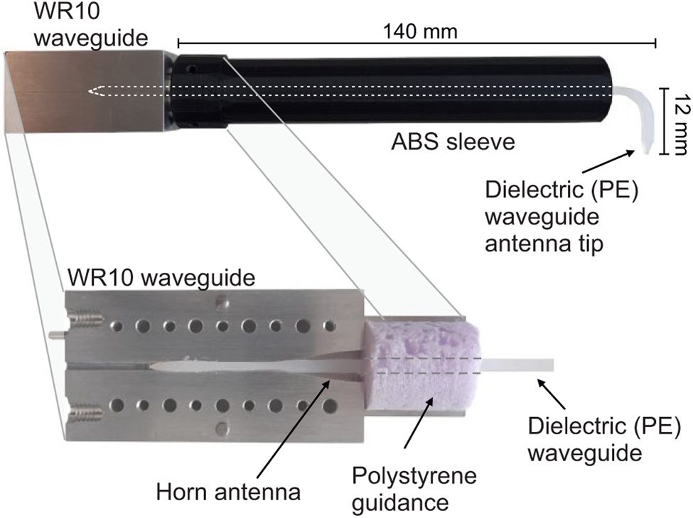
Fig. 3. WR10 metal waveguide with horn antenna and with attached dielectric PE antenna. The magnified image at the bottom shows the dielectric waveguide inserted into the hollow metallic waveguide. The dashed lines indicate the position of the dielectric waveguide where invisible.
Coupling between the dielectric waveguide and the hollow metal waveguide is implemented according to the examples in Refs [Reference Yeh and Shimabukuro13, Reference Yeh, Shimabukuro and Siegel19, Reference Weinzierl, Fluhrer and Brand20] for low-loss dielectric materials, where power coupling efficiencies up to 98% to the dielectric waveguide antenna have been reported. The WR10 coupling waveguide flange consists of a hollow metal waveguide transforming into a corrugated horn antenna at the end. In its current form, the waveguide antenna was cut from a plate of PE material to avoid internal material stress by later bending. It was then inserted into the waveguide flange extending into the rectangular waveguide region. On this end, the waveguide is slightly tapered to reduce coupling reflections of the incident waves. The flange itself can then easily be attached to the terahertz transceivers waveguide output. After leaving the waveguide region, the dimensions of the dielectric waveguide are slightly increased to a 2 × 3 mm2 cross-section. Such a coupling approach is promising for dielectric materials where roughly $\epsilon _1 / \epsilon _0 < 3$ which is the case for PE with $\epsilon _1 \sim 2.3$
 [Reference Jin, Kim and Jeon27] surrounded by air (for more details see Ref. [Reference Yeh and Shimabukuro13], Ch. 3, p. 85). At the end of the waveguide antenna, we chose a so-called x-tapered tip design for our dielectric antenna [Reference Bauer, Matheis, Mashkin, Krane, Pohlmann and Friederich9], which has been reported to yield good beam shapes and low signal attenuation [Reference Weinzierl, Fluhrer and Brand20, Reference Weinzierl, Richter, Rehm and Brand21]. In addition, this shape is much easier to fabricate than more complex tip shapes with relatively insignificant improvement in signal performance.
For our specific application scenario, we had to implement the dielectric antenna tip with a smooth angle of 90 degrees at the end. Although this will certainly give rise to some radiative losses [Reference Yeh and Shimabukuro13], we found little difference in the imaging performance compared to straight antenna tips. To still get an impression on the coupling and bending losses of our waveguide antenna realization, we carried out a transient EM field simulation of an antenna structure similar to the one employed in our measurement system. Figure 4 shows the results of the simulation which was implemented based on the OpenEMS software package [28]. In order to save some simulation time, the straight section of the dielectric waveguide was shortened compared to the actual manufactured version of the measurement system, which should be justified in the case of the low-loss PE material of our waveguide. In the simulation, the metal waveguide flange was excited by a rectangular waveguide port with a Gaussian-shaped pulse excitation with 95–105 GHz bandwidth. The electric field amplitudes in the figure were evaluated at the center frequency of 100 GHz. The figure shows the maximum electric field amplitude obtained in the x-z plane of the waveguide over all transient time steps of the simulation. We find, that some coupling losses as well as bending losses can be recognized in the simulation results. At the end of the antenna tip, the field amplitude is reduced by roughly −5 dB compared to the excitation signal. From this simple simulation approach we expect an overall power loss on the order of −10 dB compared to the signal fed to the waveguide flange. As will be shown in section “Terahertz NDT measurements”, however, we do not need to operate our system at the very limit of its available dynamic range, so that the bending losses will not significantly affect the quality of the NDT measurements. We note, however, that this may well be the case in other scenarios where thicker layers of material have to be penetrated and measurements close to noise floor should be performed. In this case, approaches to minimize bending losses should be investigated.
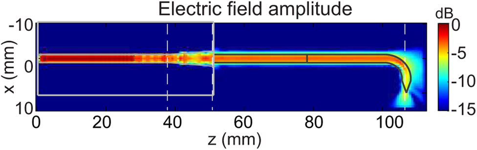
Fig. 4. Results of a transient EM simulation of the dielectric waveguide made from PE and coupled to a waveguide horn flange. The image shows the maximum of the electric field amplitude at each position over all transient simulation time steps. The first vertical dashed line at z = 40 mm marks the position of the transition from hollow to dielectric waveguide, the second line marks the end of the waveguide horn. The third line marks the position of the antenna tip.
Imaging resolution
In order to evaluate the performance of our dielectric antenna in imaging applications, we performed imaging of a metallic USAF-1951-style resolution pattern on FR4 substrate. For this purpose, the FMCW transceiver with attached dielectric waveguide antenna was mounted on an x-y translation stage to raster scan the dielectric tip over the target. Figure 5 shows the recorded images at the surface of the flat pattern recorded with our 100 GHZ FMCW system at –6 dB dynamic level in both systems. For the first measurement (Fig. 5(a)), the transceiver was first equipped with a quasi-optical PTFE-lens combination of 100 mm focal length for beam collimation and 50 mm focal length for tight focussing (see inset photograph). For the second measurement (Fig. 5(b)), the quasi-optics were replaced with a PE dielectric antenna with 90 degree bend at the end (see inset photograph) and the antenna tip was placed close to the resolution pattern's surface. A significantly improved image resolution in the near-field case of the dielectric waveguide configuration is apparent. While in the lens image the metal lines can be distinguished down to a linewidth of 2 mm (pattern element –2/1, yellow circle), the three metal lines in pattern element –2/5 with a linewidth of 1.25 mm in the dielectric tip image can still be resolved (green circle). Thus, besides the technical aspects of limited measurement space discussed above, employing the dielectric waveguide antenna in a near-field imaging configuration also significantly enhances the image resolution of the terahertz system compared to a quasi-optical setup.

Fig. 5. Resolution pattern recorded with the terahertz FMCW transceiver with 100 GHz center frequency and in two imaging configurations. (a) Measurement with quasi-optical lens setup (see inset) of a collimating (f = 100 mm) and focussing lens (f = 50 mm) resulting in a minimum distinguishable −6 dB linewidth of ~2 mm (yellow circle). (b) Measurement with dielectric waveguide antenna with 90 degree tip angle (see inset) resulting in a minimum distinguishable –6 dB linewidth of ~1.25 mm (green circle).
We note that the unfocused, near-field scenario of measurements with a dielectric tip should have some limitations regarding the distance of the tip to the test object's surface, or to deeper layers in a depth resolved FMCW measurement, respectively. For our specific measurement application of relatively thin insulation thicknesses of roughly 15 mm on top of a metal conductor, we did not recognize a significant degradation in image resolution. We are currently conducting further investigations in order to be able to quantify this aspect for future application scenarios. As a general conclusion, the versatility and relatively straight-forward fabrication of dielectric waveguide antennas makes this system approach an ideal candidate for NDT terahertz imaging wherever sub-wavelength resolution is desired and/or where free-space, quasi-optical approaches are somehow unfeasible.
Terahertz NDT measurements
In this section we present our latest results of terahertz NDT measurements with the system design as described in the previous sections. Up until this stage, the experiments were carried out in a laboratory environment. For imaging purposes, the whole transceiver unit with the attached dielectric waveguide antenna was mounted on an x-y translation stage for raster-scanning over the various samples. We are currently preparing an enhanced mechanical automation system in order to allow for measurements in-situ on a full-scale generator on site.
Model samples
We performed a number of preliminary studies to evaluate the potential of defect recognition of our NDT terahertz system. For this purpose, we first investigated a set of model samples designed to resemble typical compositions of mica insulation surrounding generator bars in real-life scenarios. In a second round of studies, we implemented some artificial defects in a real generator bar's insulation to assess the system performance in realistic measurement scenario.
Different setups of mica insulation
The mica insulation of generator bars can be implemented in different specific configurations, depending on the details of the exact application environment. We therefore carried out several test measurements on model samples with implemented defects as mockups of these different scenarios. Figure 6 illustrates three typical types of mica insulation on top of a metal conductor, represented here as an aluminum bottom layer. In all three samples, a 1 mm wide gap was implemented during fabrication of the samples to reproduce the typical dimensions of cracks forming inside the insulation. In configuration A, the mica is applied on top of some primary layers of glass fiber-reinforced plastic (GFRP) material. The implemented crack is located directly on top of the GFRP layers. Configuration B illustrates a composition of several layers of pure mica insulation where the defect is located in between the mica layers. Configuration C emulates the scenario where a crack forms under the mica insulation in direct contact to the metal base.

Fig. 6. Schematic drawings of three typical configurations of the mica insulation of generator bars and with artificial gap defects with a width of 1 mm. The test samples were fabricated on aluminum sheets to resemble the conductor plane of the bars.
We applied raster scan imaging to the model samples with a terahertz FMCW transceiver operating at 100 GHz center frequency as in the configuration described in section “Terahertz FMCW measurement system with dielectric waveguide antenna”. Figure 7 shows the resulting terahertz images of the three samples labeled A,B, and C, respectively. The photograph in the top left corner is an exemplary photograph of one of the samples of 70 × 100 mm2 size (note that for real generator bars, the mica insulation is covered with a final layer of opaque tape and the defects cannot be visually identified as in these model samples). For all three configurations of the insulation layers, the gap defect is clearly reproduced in the terahertz images with good spatial resolution. The defects can also be recognized in the corresponding B-scans. Throughout the measurements, the dielectric waveguide antenna's 90 degree tip was kept at a minimum distance of a few millimeters above the samples’ surfaces. Recall that the FMCW measurements yield volumetric data of the samples under test and that the displayed terahertz images are cross-sectional images (sometimes referred to as C-scans) evaluated at the red dashed lines in the corresponding B-scans showing the depth layers of the samples.
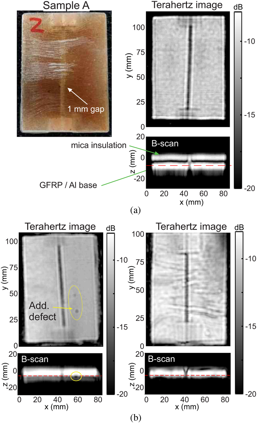
Fig. 7. Terahertz images of model samples fabricated according to the schematics in Fig. 6. Top left corner: Photograph of one of the model samples with 1 mm implemented gap defect. All defects are clearly reproduced by the terahertz NDT system. Some unintentionally fabricated defects can also be recognized in sample B (yellow circle).
We note that all implemented gaps had a width of 1 mm, which is well below the free-space wavelength of the 100 GHz transceiver unit of roughly 3 mm. We also recognize some additional defects of even smaller size in sample B which occurred unintentionally during sample fabrication. In comparative studies (data not shown) we investigated the robustness of the measurement principle under varying measurement distances and angles, since the samples under investigation may not always be perfectly flat. We find that the implemented gaps of 1 mm size can still be well-recognized at measurement angles of up to 15 degrees and distances of around 20 mm. With this proof of principle we show that our measurement approach is suitable to detect relevant defects in the mica insulation of generator bars.
Generator bar with artificial defects
We then transferred our measurement principle to realistic samples of generator bars with mica insulation and covered by an opaque tape. A number of artificial defects were implemented into the bar's insulation, as shown in Fig. 8(a). The first defect simulates a surface damage of the tape cover (#1). Next, a hole of 2 mm diameter was drilled into the insulation to represent a defect at the bar's edge (#2). Finally, a deep cut from a box cutter knife (#3) in the insulation is supposed to resemble a thin cracking of the mica layers extending from the surface down to the copper conductors. The bar was then mounted onto a second bar yielding a realistic measurement situation with limited space between adjacent bars as shown in Fig. 8(b). For the measurement, the transceiver was mounted on a mechanical x-y stage to raster scan the dielectric waveguide tip over the bar's surface.
Fig. 8. (a) A generator bar with a number of implemented artificial defects. (b) Photograph of the measurement setup resembling the real-world scenario of NDT in between adjacent generator bars.
The resulting terahertz images are displayed in Fig. 9. Again, the FMCW measurement principle allows a layer-by-layer inspection of the insulation down to the bar's metal core. The images show two cross-sectional (C-Scan) images from depths of 1 and 15 mm below the bar's surface. In the left image, the rectangular surface defect (#1) is clearly identified against the intact surface. The beginning of the deep knife cut (#3) can also be recognized in the same image. In the right image from the deeper layer of the insulation system, the knife cut (#3) is even more pronounced and the drill hole (#1) is clearly visible. We also note that these images are further proof that even in this near-field measurement scenario, a high-resolution inspection down to the bar's metal core with roughly 15 mm distance to the dielectric antenna tip is indeed possible.
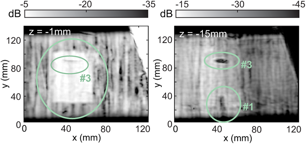
Fig. 9. Terahertz images of the generator bar from two different depth cross-sections (z=−1 mm and z = −15 mm) below the surface. All implemented defects are clearly recognized in the terahertz images.
Real defect in a generator bar
We finally applied our terahertz NDT measurements to generator bars with real defects from operation in a power plant. The bars have been identified to contain cracks in the mica insulation and were then cut out from the stator for further investigation. Figure 10 shows in the top image a photograph of a bar where a defect can already be suspected from visual inspection of the tape cover. The X-ray images at the bottom confirm that a crack indeed extends through the entire insulation system down to the conductor. Besides the quite large efforts required to remove the bar from the generator to perform X-ray CT imaging, the images also lack in contrast which can make identification of defects rather difficult. The same bar was then inspected with the terahertz NDT system with dielectric waveguide antenna in a setup similar to the one in Fig. 8(b) (but without a second attached bar).

Fig. 10. Generator bar with real crack already visible from the outside. The x-ray cross-section images show the extension of the crack from the copper conductor through the mica insulation up to the surface.
Figure 11 shows two terahertz images of the bar with defect at two depth layers, namely at the surface with the cover tape (top image) and at the layer of the conductor at about 14 mm below surface (bottom image). In the top image, the ruptured tape can be recognized where the internal crack had extended up to the surface. The bright vertical stripe represents a piece of aluminum tape to mark the position for the previous x-ray scans. In the bottom image, the crack in the mica insulation can be clearly identified, also confirming its extension down to the conductor plane. Here, the aluminum tape shows as a dark vertical stripe because all terahertz radiation is reflected off the tape at the surface. We also make the interesting observation that the deeper crack seems to follow a slightly different curvature than the optically visible rupture of the cover tape at the surface. This finding emphasizes the importance of depth-resolved measurements by the FMCW principle to be able to resolve the direction of internal defects at different layers in the volumetric terahertz data. Note the high dynamic range in the terahertz images, where even at around −50 dB intensity level, no noise background is visible. Thus, the bending losses of 5–10 dB in field magnitude mentioned in section “Terahertz FMCW measurement system with dielectric waveguide antenna” can easily be accepted in this particular application scenario. Finally, with these measurements we could show that real defects in generator bars can be clearly resolved in terahertz FMCW measurements with a dielectric waveguide antenna for on-site NDT inspection purposes.

Fig. 11. Terahertz images of the generator bar with crack defect (see Fig. 10). The top image shows a cross-section just below the insulation surface, where the rupture in the orange tape cover is recognized. The bottom image shows the actual crack in the mica insulation at a deeper layer close to the surface of the center conductor. The crack can be clearly identified to extend above the full width of the bar and extending through the whole insulation.
Conclusion and outlook
In this paper we have shown the development and successful application of a terahertz FMCW transceiver with attached dielectric waveguide antenna for NDT inspection. Our system is based on the combination of a 100 GHz FMCW transceiver and a low-loss dielectric waveguide antenna with a 90 degree tip at the end to enable terahertz measurements in environments with only limited access space. Efficient power coupling is achieved by integrating the dielectric waveguide into a WR10 waveguide horn antenna. We showed that the concept of near-field raster scanning over a sample allows the recording of volumetric terahertz images with sub-wavelength resolution. In test measurements we could achieve a lateral resolution around 1.25 mm which is well below the free-space wavelength at the employed working frequencies between 70 and 110 GHz. We optimized the geometry of our dielectric waveguide antenna for the specific application of the in-situ NDT inspection of the mica insulation of generator bars of turbogenerators in power plants with limited available measurement space between adjacent bars. After demonstrating the potential of the measurement technique on a number of model samples, we finally showed that the developed terahertz NDT system can detect real-world defects in the mica insulation of generator bars containing surface and sub-surface cracks. Altogether, terahertz FMCW measurements in combination with the versatility and enhanced resolution of dielectric waveguide antenna can be a powerful tool for NDT imaging where high resolution is desired and where limited access to the objects under test may prevent the use of classical quasi-optical beam focusing approaches. We emphasize that this system approach is, however, not limited to the above, restrictive case scenarios, but should rather be considered a noteworthy alternative concept for terahertz NDT imaging, in particular when thin objects of few centimeters thickness are investigated. Typical scenarios could be layered materials such as GFRP composites for lightweight construction or various types of coatings for both electrical or thermal insulation.
We are currently implementing a fully automated scanning mechanic to be placed in front of the generators and with the ability to inspect the relevant areas of the stator bars on site. To achieve a constant distance of the waveguide tip to the bar's surface inside the interspace between bars, a bent mechanical translation stage is manufactured to follow along the curvature of the bars. Figure 12 shows a CAD image of the designed mechanics which are currently being manufactured. It should be noted that in general, the aforementioned benefits of the presented near-field NDT approach come with challenges to keep a fixed distance of the dielectric tip to the target for uneven surfaces – at the least, to avoid physical collision with the target. Here, quasi-optical imaging systems can sometimes provide a slightly relaxed constraint due to their depth of focus at lower terahertz frequencies and the larger distance to the target. It is the subject of our ongoing research how strong distance variations between dielectric waveguide tip and target surface affect the achievable lateral resolution of the acquired terahertz images.
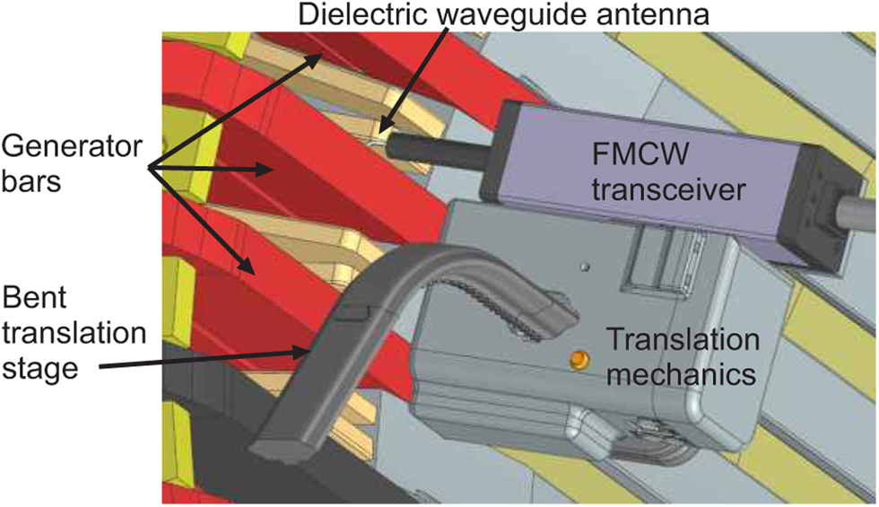
Fig. 12. CAD design of the scanning mechanics for an automated inspection of the generator bars on site in power plants.
On the system side we are further investigating the coupling efficiency and reduction of bending losses in the current implementation of the dielectric waveguide antenna. Here, dielectric waveguides with a metal coating could help to further improve the guiding properties of our near-field antenna. We are also looking into fabrication techniques such as 3D printing methods like selective laser sintering which could make the production process of dielectric waveguides even more reliable for large-scale production. Recently, we presented two machine learning (ML)-based approaches for the evaluation of terahertz image data [Reference Bauer, Hussung, Matheis, Reichert, Weichenberger, Beck, Matuschczyk, Jonuscheit and Friederich8, Reference Sharma, Hussung, Keil, Friederich, Fromenteze, Khalily, Deka, Fusco and Yurduseven29]. In the specific example of generator bars, ML techniques could be used to separate possible crack signatures in the terahertz images from the background of the copper conductors and the windings of the outer tape cover. Eventually, such techniques could greatly support the automated processing of terahertz images, where a manual inspection of the amount of NDT images of an entire turbogenerator could be too time consuming for human operators.
Acknowledgements
We thank our colleagues Luca Lersch, Luka Maxim Obermayr, and Stefan Obermayr at Siemens Energy for their efforts in the design and fabrication of the mechanics for automation of the measurements.
Conflict of interest
None.
 Maris Bauer was born in 1985 in Frankfurt am Main, Germany. He received his doctoral degree from Goethe-University Frankfurt, Germany, in 2018 working on the modeling of charge carrier transport and photo-thermoelectric effects in TeraFETs, and the implementation and characterization of devices in different materials including novel carbon-based materials and III-V semiconductors. From 2008 to 2014 he has been with SynView GmbH as a research assistant. In 2017 he joined the Center for Materials Characterization and Testing, Fraunhofer ITWM, Germany, working on terahertz applications and system design.
 Raphael Hussung received the Bachelor of Science (B.Sc.) and Master of Science (M.Sc.) degrees in electrical engineering and computer engineering from TU Kaiserslautern, Kaiserslautern, Germany, in 2018 and 2020, respectively. During that time, he worked part-time with Pollux Electromechanical Systems GmbH, Kirchheimbolanden, Germany, a supplier of conditioning systems for the automotive industry, where he was tasked with hard- and software development. He joined Fraunhofer Institute for Industrial Mathematics, Kaiserslautern, as a Research Associate, in July 2020. His research interest includes millimeter wave and terahertz imaging with multistatic sensor arrays for non-destructive testing applications.
 Carsten Matheis worked as a metal cutting mechanic until 2003 when he joined Fraunhofer IBMT, St. Ingbert, Germany, to complete his training as a microsystem engineer in 2005. He's been with Fraunhofer IPM, Kaiserslautern, Germany since 2005. In 2017, the Department of Materials Characterization and Testing was formed at Fraunhofer ITWM, Kaiserslautern, Germany, where he has since been working as a technical assistant in the field of terahertz applications for non-destructive testing.
 Andrey Mashkin Andrey Mashkin did his master thesis and Ph.D. in High Voltage and Insulation Technology at RWTH Aachen University on novel insulation materials. His field of interest within Siemens Energy covers innovations on insulation systems, insulation assessments, and diagnosis and novel energy storages.
 Stefan Krane joined Siemens Energy in 2008 for an apprenticeship and dual studies program. He received his Bachelor of Electrical Engineering in 2012 and his Master of Engineering in 2015 from the University of Applied Sciences Gelsenkirchen, Germany. During his studies, he focused on power engineering, energy system engineering, and turbomachines. Since 2009, he is working in the High Voltage and Insulation Technology Department within the Generator Engineering in Muelheim, Germany, where his tasks include electrical diagnosis and evaluation of the insulation of generators.
 Friedhelm Pohlmann received the Dipl.-Ing. degree in electrical engineering from Technical University of Brunswick, German, in 1995 and a Ph.D. from the University of Essen, Germany, in 2001. He joined Siemens AG, Energy Sector (now Siemens Energy) in March 2002 and worked as a development engineer in the field of aging mechanisms and electrical testing of rotating machine insulation. In 2007, he became head of the High Voltage and Insulation Laboratory and since 2009 he is head of the High Voltage and Insulation Technology Department within the Generator Engineering in Muelheim, Germany.
 Fabian Friederich Fabian Friederich graduated in optoelectronics at Aalen University of Applied Sciences, Germany, in 2007, and received the Ph.D. degree in physics from Goethe University, Frankfurt am Main, Germany, for his work in the field of terahertz imaging with the Ultrafast Spectroscopy and Terahertz Physics Group, in 2012. During his studies, he was also associated with the Centre for Micro-Photonics, Swinburne University of Technology, Melbourne, Australia, and with the Laser Zentrum Hannover e.V., Germany. In 2011, he joined the Institute of Technical Physics, German Aerospace Center (DLR), Stuttgart, Germany, to establish laser-based concepts for monitoring space debris. In 2013, he was granted a Fraunhofer Attract Funding to form a new research group in the field of millimeter-wave and terahertz measurement techniques at Fraunhofer IPM, Kaiserslautern, Germany. Since 2017, his group has been with Fraunhofer ITWM, Kaiserslautern, Germany, pursuing its millimeter-wave and terahertz activities in the field of non-destructive testing.


 Open access