


Introduction
Chiplessradio-frequency identification (RFID) systems are expected to revolutionize the predecessor's automatic identification technologies [Reference Khaliel1]. However, the system is still at the conceptual level and could not be exploited to the full potential in low-cost item tagging due to the following handicaps. The first one is the low value of the tag radar cross section (RCS) results from the small tag size. Moreover, the tag backscattering signal is subjected to a fourth power reduction in magnitude with the reading distance. The second challenge, is the environmental reflections which are contaminating the tag backscattering signal [Reference Fawky2] and this makes the tag unreadable even if it is within the reader reading range. The last major problem is the multi-tag interference [Reference El-Hadidy3]. The superposition of the tags responses within a specified interrogation zone cannot be discriminated if the number of tags exceeds an absolute limit. These limitations are addressed in the literature from the signal processing point of view [Reference El-Hadidy3, Reference Rubayet-E-Azim, Karmakar and Amin5, Reference Rezaiesarlak and Manteghi6]. Moreover, the spatial division multiple access is proposed for the time coded chipless RFID tags [Reference Anee and Karmakar7].
On the contrary, these aforementioned frequency coded (FC) chipless RFID handicaps are solved in the work of this paper from the following scopes:
(i) RA Readers: RA antenna is proposed to improve of the chipless RFID reader antenna system [Reference Khaliel1]. This RA antenna system plays a significant role in increasing the tag reading range and enables the tag detection in a real environment. Furthermore, the contamination of tag response due to the multi-path clutter components is dramatically reduced while exploiting the pencil beam provided by the RA antenna.
(ii) Chipless RFID Tags: The designed tag is implementing the collision avoidance medium access control (MAC) protocol introduced in [Reference El-Hadidy3], which mitigates the multi-tag interference by introducing notch position modulation (NPM) scheme for the tag code.
The introduced work is organized as follows. In the section “Tag design and problem description”, the tag design and the problem description are explained. The fundamentals and limitations of the RA antenna are explored in the section “The fundamentals and limitations”. The design guidelines, and the analysis methods are illustrated in the section “Design guidelines and analysis methods”. Thesection “The developed fixed beam RA antenna” introduces the developed fixed beam RA antenna. The integration testbed is demonstrated in the section “Realistic testbed: chipless RFID tags and UWB RA antenna”. Finally, the conclusion is presented in the section “Conclusion”.
Tag design and problem description
In this section, the tag design is introduced. After that, the multi-tag interference problem is discussed with the aid of Electro Magnetic (EM) simulations. Then, the reading range calculations are presented.
NPM position modulation tags
The NPM is a collision avoidance physical modulation scheme which is introduced in [Reference El-Hadidy3, Reference Khaliel4]. In this scheme, each notch position resembles a tag coding bit where the presence of a notch resembles the logic-1 and the absence resembles the logic-0. The introduced tag consists of coplanar ring resonators without ground plane. Each ring resonator symbolizes a tag coding bit where the ring radius is determined by:
 $$ R = \displaystyle{{c} \over {2\pi f_{0}}} \sqrt{\displaystyle{2} \over {\epsilon _{reff} + 1}}, $$
where f 0 is the resonance frequency, c is the light speed, ε r is the substrate relative permittivity, and R is the ring radius. The advantage of the ring structure is that the spurious harmonics are not generated because of the structure symmetry [Reference Islam17]. Furthermore, the coding bits can be increased without significant increase in the tag size by adding extra rings. Therefore, the tag structure is scalable and printable.
Three key features are introduced to the new enhanced tag design. The first one is adding redundant deactivated rings in between the coding ones to minimize the notch width, increase the number of coding bits, and thus conserve the spectrum. The conventional encoding methodology to switch off a notch is to remove the corresponding ring, as described in [Reference Islam17]. However, the RCS resonance bandwidth is highly affected by the presence or absence of the adjacent resonators. The notch width gets wider if the surrounding notches are removed. Thus, a novel encoding methodology is introduced to preserve the current distribution and so the bandwidth. This methodology is based on introducing a cut in the ring current path in two orthogonal directions to remove the corresponding notch from the coding spectrum without removing the corresponding ring as described in [Reference Islam17]. The last feature is to boost the level of the backscattered power by designing (2 × 2) tag array. This array increases the value of RCS by 6 dBsm at the expense of increasing the tag size.
The single manufactured tag as shown in Fig. 1 illustrates the novel encoding methodology and the inserted supplementary resonators.

Fig. 1. NPM RCS manufactured tag.
Problem description
Basically, the environmental clutter reflections are stronger than the tag response and thus conceal the tag response. Therefore, reducing the cluttering signals is utmost important. Moreover, the multi-tag interference is also contaminating the tag's RCS frequency response. Therefore, the multi-tag interference problem is studied using EM simulations, where multiple NPM RCS tags with various codes are simulated simultaneously. The simulation setup consists of two different tags separated by a minimum distance d as shown in Fig. 2. This separation is determined from the far-field classical equation ( $ d = {\displaystyle {2D^2} \over {\lambda}}$, where D is the largest tag dimension) and also verified by the full wave simulation. Therefore, the minimum separation between the tags is calculated to be 6 cm. So, various tags are added in the simulation environment with 6 cm separation. It is observed that, if the tags are with the same code the RCS level is directly related to the tags quantity. However, if the tags are different codes as explained in Fig. 3, the notches are interleaved with each other producing a large notch at the whole band and the frequency position of the produced notch is not deterministic. One possible solution to mitigate this problem is to make the resonance bandwidth very narrow with sharp cutoff characteristics. However, this ideal notch features cannot be achieved. Therefore, decreasing the number of tags in the reader interrogation zone is very important.

Fig. 2. Multi-tag interference simulation setup.

Fig. 3. Multi-tag interference simulation study for: (a) two tags with different codes. (b) Three tags with different codes.
The other major limitation of the chipless RFID system is the short reading range which is few centimeters <40 cm [Reference Khaliel, El-Hadidy and Kaiser8, Reference Khaliel9]. This reading range is estimated using equation (2), considering symmetrical system, i.e., the reader's transmitting and receiving antennas are at the same position:
 $$ r_{\rm range} = \root 4 \of {\displaystyle{{G_TG_R\lambda ^2PT} \over {{(4\pi )}^3P_r}}} \sigma, $$
where r range is the tag reading distance, G T is the gain of transmitting antenna, G R is the gain of receiving antenna, λ is the wavelength, σ is the tag RCS, P R is the reader received power, and P T is the reader transmit power which is restricted by the Federal Communications Commission (FCC) ultra wideband (UWB) power regulations. In [Reference Mohamed10] a novel interrogation methodology is proposed to increase the reader transmit power by best utilizing the UWB power regulations. This methodology states that 0 dBm peak level of emission is allowed within 50 MHz bandwidth [11]. Therefore, a frequency sweeping mechanism is used to interrogate the tags instead of the UWB pulse transmission which is limited to −41.3 dBm/MHz, i.e., −24.31 dBm/50 MHz. Therefore, this methodology is applied on the proposed NPM tag where the RCS value of the logic-1 is −30 dBsm and that of the logic-0 is −10 dBsm. The reading distance is calculated at 5 GHz assuming unity gain transmitting antenna (G T = 0 dBi) and that the receiving antenna gain is (G R = 10 dBi), as shown in Fig 4. In order to be able to detect the notch precisely, at least 5 dB dynamic difference is required between the notch and the peak level. Therefore, considering that the receiver sensitivity is −80 dBm, the minimum RCS value that can be detected at 2 m is about −20 dBsm and thus the notch dynamic range is −10 dB. However, this theoretical reading range cannot be reached in a real-world scenario because of the cluttering signals, the transmitter leakage, and so on.

Fig. 4. Theoretical reading range as a function of the received power at 5 GHz in case of: (a) UWB transmission with −41.3 dBm/MHz, (b) frequency sweeping interrogation with 0 dBm/50 MHz.

Fig. 5. RA building blocks.
In order to overcome the above-mentioned limitations, the reader antenna should attain the subsequent characteristics. It should operate over UWB range of frequencies to accommodate multiple bits, it should be directive to minimize the environmental reflections, and it should have high gain to increase the reader coverage. Moreover, the low cost and the capability of beam-steering are also very important features. Therefore, the single antennas, the parabolic reflectors and the phased array antennas have little acceptance in the chipless RFID systems, specifically in the supermarket scenario. In this regard, the RA antennas are proposed in this paper to be used for the supermarket scenario due to the next reasons. The first one is that the RA antenna is more directive and higher gain than the single antenna element, like the horn antenna. The second one is that the RA antenna is completely planar surface, lighter weight in comparison with the bulky parabolic reflectors which are also incompetent for beam steering. Another advantage is the comfortability with installation platforms (conformal geometry), which enables the RA surface to be customized according to the geometry and space available. On the other hand, in case of the parabolic reflector the beam focusing is emanated from the parabolic geometry as known. In comparison with the phased array antenna, the RA antenna can operate over UWB range of frequencies with low cost because of the exclusion of the complex feeding network. Therefore, the spatial feeding RA antenna is the best candidate in comparison with the bulky reflector and the complex feeding network phased array antennas. However, there are challenges that impede the RA antenna employment, which are addressed in the next section.
RA fundamentals and limitations
RA is a hybrid antenna system which combines the favorable features of the parabolic reflector and the phased array antennas. These combined advantages are the spatial feeding, the lightweight, the multi-beam capability, and the low cost. The RA antenna consists of free space located feeder which spatially illuminates a flat reflecting surface of radiating cells as shown in Fig. 5. The power received by each cell is re-radiated after modulating the reflection phase. Therefore, the re-radiation characteristics are controlled by tuning this reflection phase distribution over the array surface which re-radiates the incident energy in a single beam or multi-beams with arbitrary beam shape and direction.
There are two factors which limit the RA antenna bandwidth. The first one is the phase delay difference between the feeder phase center and each point on the RA surface. The second factor is that the RA cell exhibits narrow-band resonance, and this factor is dominant for moderate size RA antennas with size < 20λandFocal/Diagonal > 0.5 [Reference Shaker, Chaharmir and Ethier13]. Basically, using single resonator as an array element offers one resonant frequency. Consequently, the phase range is <360°, the phase slope is nonlinear and thus the operating bandwidth is narrow with high scattering field components. Recently, several efforts have been devoted to enlarge the RA antenna bandwidth such as using multi-layer stacked resonators, aperture coupled elements [Reference Tahseen and Kishk12]. But these proposed solutions are suffering from labor intensive manufacturing process. Recently, utilizing single layer concentric or non-concentric resonators can enhance the RA antenna bandwidth [Reference Khaliel1, Reference Guo, Tan and Chio14, Reference Florencio15]. Moreover, using thick material substrate with low value of relative permittivity could also enlarge bandwidth. In this regard, a foam substrate is exploited to linearize the phase slope and to broaden the bandwidth as will be explained in the following sections.
Design guidelines and analysis methods
There are two approaches which can be used to design RA antenna. The core functionality of these approaches is to calculate the cell reflection phase curves with the physical or electronic tuning parameters. The first approach is based on calculating the field distribution at the array plane while illuminating the array surface with a predetermined feeder radiation pattern. The other approach is based on the approximation of normal plane wave excitation and local periodicity where all the RA cells are assumed to be identical. For both approaches the RA cell is determined first. The cell parameters are the substrate materials, the cell shape, the cell dimensions, and orientations. Therefore, these parameters can be exploited for minimizing the backscattering losses and linearizing the reflection phase slope as explained previously. After obtaining the best cell specifications, the tuning parameters which can be physically or electronically controlled are determined, and the reflection phase curves are calculated in accordance with the variation of these parameters. Hence, the compensating phase curves are derived at the design frequencies, which are, in our case, the center and edge frequencies. Consequently, the developed Matlab algorithm calculates the required compensating phase distribution on the array surface. These calculations take into account the other parameters which are (the number off cells, the number of beams, the direction of the generated beams, and the feeder configuration). After that, the calculated phase distribution is realized exploiting the tuning parameters set, and thus, each cell is realizing a predetermined reflection phase values. Finally, the feeder is designed and the complete array is integrated, simulated, optimized, and analyzed for performance prediction.
The initial phase distribution for each cell is calculated by equation (3).
 $$\eqalign{& \phi _R(x_{ij}, y_{ij}) = \cr & \quad k_0(d_{ij} - (x_{ij}{\rm sin}\theta _b{\rm cos}\phi _b) - (y_{ij}{\rm sin}\theta _b{\rm sin}\phi _b)),} $$
where ϕ R(x ij, y ij) is the phase of the reflected field, k 0 is the propagation constant in vacuum, d ij is the distance from the feeder phase center to the array cells, (x ij, y ij) are the coordinates of element (i, j) and (θ b, ϕ b) are the elevation and azimuth angles of the produced beam, respectively. The minimum distance between RA cells that avoid the appearance of grating lobes is calculated based on equation (4)
 $$ {\displaystyle{d} \over {\lambda_{0}}} \les \displaystyle{1 \over 1+\sin(\theta) }, $$
where d is the element spacing, and θ is the angle of the feeder incident beam. Therefore, the elements located at the RA edges are better to be larger spacing. However, uniform spacing is used to simplify the design procedures.
Analysis methods
The factors that gauge the RA antenna performances are the aperture efficiency, the phase errors, cross polarization level, the losses, and the feeder blockage [Reference Shaker, Chaharmir and Ethier13]. The mathematical expressions for these terms are expressed for analytical analysis of the RA antenna performance. The first factor is the aperture efficiency, which is expressed in equation (5) [Reference Balanis16]:
 $$ \eta_{\rm aper}\approx\eta_{s}\eta_{t}, $$
where η aper is the aperture efficiency, η s is the spillover efficiency, and η t is the taper efficiency. Considering that the feeder pattern is cos n(θ), the spillover efficiency is calculated based on equation (6) [Reference Shaker, Chaharmir and Ethier13]:
 $$ \eta_{s}=1-\cos^{n+1}(\psi _{RA}/2), $$
where (ψ RA) is the subtended angle of the RA. In a similar way the taper efficiency is driven in [Reference Shaker, Chaharmir and Ethier13]:
 $$ \eta_{t} = {\displaystyle{2n\,(1-\cos^{n}(\psi _{RA}/2))^{2}} \over {\tan^{2}(\psi _{RA}/2)\left [ \displaystyle{n} \over {2} -1\right ]^{2} 1-\cos^{n}(\psi _{RA}/2)}}. $$
Therefore, a judicious design of the RA surface yields a good aperture efficiency and the best F/D ratio is determined from the optimum subtended angle.
The polarization efficiency of the RA is expected to be high even if the feeder is low cross-polarization level. This is because the RA constituent elements are polarization selective dissimilar to the parabolic reflector. The phase efficiency is determined from the phase error terms mentioned before. These error terms get worse for large RA aperture size except the terms of local periodicity assumption. Consequently, the bandwidth is reduced. The maximum value effect of phase errors is 180° that value causes out of phase radiation. Therefore, these RA antenna analysis terms can be estimated numerically using array theory and verified with the full wave simulation.
The developed fixed beam RA antenna
This section presents the developed fixed beam RA, where the printed elements located on the array surface impart a given phase onto the incoming wave physically. In this regard, a developed UWB RA dedicated to the chipless RFID applications is demonstrated.
Cell Features and Design Key Points
The ideal RA cell re-radiates the incident wave with zero attenuation and linear reflection phase curve with sufficient range to avoid approximation and truncation errors. In this paper, the circular rings are proposed to constitute the RA cells as illustrated in Fig. 6. Although, the ring structures are narrow band, the resonance bandwidth can be increased by increasing the substrate thickness and reducing the effective permittivity. Therefore, a low relative permittivity substrate is loaded with a foam layer to enlarge the resonance bandwidth, minimize the re-radiation losses, and linearize the phase slope. Furthermore, the inner and outer ring dimensions which provide sufficient phase range and linear phase slope are initially calculated to be Rinner = 0.8 × Router, W = 0.08 × Router.

Fig. 6. Fixed beam RA antenna basic cell configuration.
UWB RA for Chipless RFID Applications
This section introduces the UWB RA antenna which is developed to be utilized at the chipless RFID reader. Therefore, the RA design objectives is to produce a high gain pencil beam pattern over UWB range of frequencies. Moreover, the design complexity and the cost features are important to be minimum. The RA cell should provide a sufficient phase range and linear phase slope if a good bandwidth is to be achieved. Furthermore, the feeder phase center position should be kept constant. Thus, the phase Figure of Merit (FoM) is defined to determine the slope of the phase curve around a certain frequency.
 $$ {\rm Phase} \quad FoM = {\displaystyle{\Delta \phi} \over {\Delta {\,f}}}. $$
The focal to diagonal ratio and the outer ring radius are optimized for a minimum value of phase FoM for each phase curve in order to get parallel phase-frequency curves as illustrated in Fig. 7. Therefore, the produced phase curves are approximately fulfilling the following equation equation (9) [Reference Chen18].
 $$ \Phi (\,f_l(n))-\Phi (\,f_l(n+1))=\Phi (\,f_u(n))-\Phi (\,f_u(n+1)), $$
where ϕ(f l(n)) is the phase value at the lower edge frequency for the element n, and ϕ(f u(n + 1)) is the phase value at the upper edge frequency for the element n + 1

Fig. 7. Reflection phase variation with frequency for different outer ring radius.
The utilized cell consists of two circular rings in a nested formation. This developed cell introduces two co-located resonances and, therefore, essentially doubles the phase range of a single resonance element. As mentioned above, the bandwidth can be increased by increasing the substrate thickness as illustrated in Fig. 8. Therefore, the substrate which is 3 mm thickness and loaded with 5 mm foam material is used for the RA design. The slow phase variation as shown in Fig. 8 provides immunity against manufacturing tolerance and truncation errors. Moreover, the F/D ratio is optimized so that the array elements in the middle are almost same size and smaller than the edge elements to reduce the coupling. This smooth variation of the cell elements across the RA surface justifies the assumption of infinite periodicity and minimize the phase errors. Therefore, the UWB RA antenna is achieved.

Fig. 8. UWB RA cell reflection phase with the outer ring radius at 5 GHz and the other cell dimensions are in relation to R outer.
An UWB horn antenna operating from 4 GHz to 6 GHz is designed, and implemented in CST to be employed as the array feeder. Furthermore, different feeder and array configurations are investigated to best emulate the real case scenarios with the appropriate configuration. Hence, the possible configurations can be Center Feed Center Beam (CFCB), Offset Feed Center Beam (OFCB), Center Feed Offset Beam (CFOB), and the simultaneous dual-beam. The CFCB configuration is not preferred because of the feeder blockage, and to minimize it, the feeder or the beam is placed or directed away from the center of the RA surface. Thus, both configurations are investigated, where the offset beam is directed towards ϕ = 0°, θ = 30°, while in case of the offset feed the beam is directed towards ϕ = 0°, θ = 0° and the feeder is placed away from the RA center. The simulated realized gain for both configurations is illustrated in Fig. 9. These results verify that both CFOB and OFCB configurations are accepted for feeder blockage minimization.

Fig. 9. Simulated realized gain patterns for the CFOB and OFCB configurations at 5 GHz.
Lastly, the dual beam generation is investigated. The RA feeder is placed at the center of the array surface and simultaneous dual-beam in different directions can be generated. This configuration is described in Fig. 10, where double beams can be achieved covering two different interrogation zones simultaneously. However, depending on the number of generated beams, the RA gain, half power beamwidth (HPBW) are reduced. Therefore, the OFCB configuration is employed for the introduced UWB RA antenna. This prototype is developed specifically for the chipless RFID applications.

Fig. 10. Simultaneous dual-beam configuration with two beams directed at ϕ = 90°, θ = 30° and ϕ = 90°, θ = −30°.
UWB RA antenna measurements
First, the designed feeder is manufactured and verified inside the Anechoic Chamber (AC), where the measurement setup of the feeder is described in Fig. 11(a). The simulated and measured radiation patterns are in a good agreement as illustrated in Fig. 12(a). After that, the RA surface which consists of 9 × 9 cells is implemented. The cell size is half wavelength at 5 GHz, which means that the total size of the RA surface is 27 cm × 27 cm. The feeder is integrated with the RA surface as shown in Fig. 11(b). The RA antenna simulations and measurements are in a good match as illustrated in Fig. 12(b). However, the RA beam is slightly shifted right beyond 5.5 GHz. This shift results from the phase errors of the realistic integration. It is clearly seen in Fig. 13 that the RA surface yields approximately four times narrower beam width and thus 6 dB higher gain than the horn antenna.
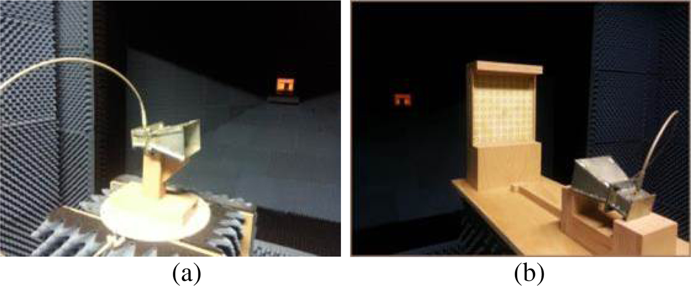
Fig. 11. Measurements setup: (a) Feeder measurement setup. (b) Complete RA antenna measurement setup inside AC.

Fig. 12. Radiation patterns simulation and measurements: (a) Feeder simulated and measured radiation patterns. (b) Complete UWB RA antenna simulated and measured radiation patterns .

Fig. 13. The measured radiation patterns of the UWB feeder vs the UWB RA antenna.
Table 1 is summarizing the features of the developed prototype from the scope of the 3-dB gain BW, the realized gain, and the aperture efficiency which are calculated at 5 GHz using equation (10).
 $$ G = {\displaystyle{4\pi } \over {\lambda ^{2}}}.\eta_{\rm aper}.A_{\rm p}, $$
where G is the realized gain, A p is the physical area.
Table 1. The characteristics of the developed fixed beam RA antenna

Realistic testbed: chipless RFID tags and UWB RA antenna
The proposed system is a preliminary design for the supermarket scenario, where the tagged items are moving on a conveyor belt through the interrogation zone of a fixed reader antenna system. Therefore, two different NPM tags are designed in the frequency range from 4 GHz to 6 GHz. After that, the complete RA antenna is integrated with the Universal Software Defined Radio Platform (USRP) to assess the design objectives with realistic chipless RFID tags in a real environment. The complete testbed is illustrated in Fig. 14, where the tags are placed in the middle distance between the transmitting and receiving RA antennas. The USRP is used for the reader implementation, in which the sensitivity is about −65 dBm and the receiving bandwidth is 40 MHz. The value of the output power is configured to comply with the UWB power regulations which allows effective isotropic radiated power (EIRP) of 0 dBm/50 MHz. The gain of the receiving antenna is 19 dBi. Therefore, the theoretical achievable reading range is 1 m in which the 20 dB full dynamic range of the notch can be detected. The dynamic range of the detected notches is reduced due to the fact that the RA antenna is not completely suppressing the environmental reflections, besides the mutual coupling between the USRP transmitting and receiving ports. Moreover, the low frequency notches are narrower bandwidth and thus less dynamic range than the higher frequency notches as clearly seen in the measurement results in Fig. 15. However, the achieved results verify the system level integration of the chipless RFID tags and the RA antenna in a real environment.

Fig. 14. Chipless RFID tags and UWB RA antenna testbed.

Fig. 15. Testbed simulation and measurement results for the first tag with code (11010101) and for the second tag (10101010).
Conclusion
In this work, a novel RA antenna is introduced to be utilized at the chipless RFID readers. The advantages of the presented high gain pencil beam RA antenna are exploited to increase the reading range and enable the tag detection in a real environment. Special considerations are devoted to design simplicity, enlarge the operating bandwidth, increase the spatial resolution, minimize the re-radiation losses, and reduce the SLL. The developed prototype exploits a designed constant phase center horn antenna to feed the RA surface. Therefore, an UWB RA antenna based on double circular ring resonator cell is demonstrated. Measurements illustrate that the bandwidth of the developed UWB RA antenna is 2 GHz fulfilling the requirements of the FC chipless RFID systems. Accordingly, multiple bits accommodation is enabled. Furthermore, the radiated beam is 15° HPBW, 19 dBi gain, and −10 dB SLL. Therefore, the developed UWB RA antenna is successfully integrated with the chipless RFID tags and a reading range of 1 m is achieved, according to the FCC regulations and using USRP transceiver.
Acknowledgments
The authors would like to thank the Institute of Digital Signal Processing, Duisburg, Germany for funding the research work introduced in this manuscript.
 Maher Khaliel (M’16) received his Ph.D. degree in 2016 in electrical engineering from the institute of digital signal processing (DSV), Duisburg-Essen University. His Ph.D. work was centered around innovating chipless RFID tags, developing the reader antenna, and integrating innovative approaches to advance the reader functionality. Within the work of his PhD, Dr. Maher published and co-authored 15 conference papers, 4 international journals, and 2 scientific workshops. He was nominated for the best student paper award at European Conference on Antennas and Propagation (EUCAP 2015 & 2017), and he got the best paper award of the 15th IEEE International Conference on Communications Systems (ICCS 2016). Prior to enrolling at DSV, he worked as a teaching assistant in Benha University, Egypt. He holds the master’s degree in 2012 in electrical engineering from Benha University. Now he is working as a senior developer at ID4us GmbH, Duisburg, Germany.
 Ahmed El-Awamry (M’15), received the B.Sc and M.Sc degrees in electrical engineering from the faculty of engineering, Benha university in 2008 and 2013 respectively. In 2016 he got his Ph.D. degree in electrical engineering from the institute of signal processing (DSV) Duisburg Essen University about chipless RFID collision avoidance MAC protocol and real world implementation. He was nominated for the best student paper award at European Conference on Antennas and Propagation (EUCAP 2015 & 2017). He worked as a lecturer assistant at the faculty of Engineering at Benha University from 2009. In addition, he worked at the Research and Development department at Elsewedy electrometer. He was responsible for North America smart meter design and development from 2008 to 2012. He worked as a research engineer at Orange labs Cairo at Machine-to-Machine team. His master thesis is funded by France Telecom at the field of designing a novel ad hoc network protocol for smart metering application in 2013. Then, he joined the CND department at American University in Cairo (AUC) as a research engineer. Currently, he is working as a senior developer at ID4us GmbH, Germany.
 Abdelfattah Fawky Megahed obtained his bachelor degree in communication engineering from the GUC (German University in Cairo), Egypt, in 2008. He then worked as a full time teaching assistant in the IET faculty in the GUC for 3 years. In 2011 he completed his master thesis in Hannover, Germany, in the topic of “Cooperative Spectrum Sensing under Deterministic Channel in DVB-T Cognitive Radio Network”. He continued his work as assistant lecturer in the GUC for 2 years. In 2013 Abdelfattah obtained a scholarship from DAAD for the project ID4Egypt and got his PhD in 2016 in the topic of “Chipless RFID Identification and Localization”. He was nominated for the best student paper award at European Conference on Antennas and Propagation (EUCAP 2015 & 2017). Now he is working as a senior RFID developer at ID4us GmbH, Duisburg, Germany.
 Thomas Kaiser (M’98-SM’04) received the Diploma degree in electrical engineering from Ruhr-University Bochum, Bochum, Germany, in 1991 and the Ph.D. (with distinction) and German Habilitation degrees in electrical engineering from Gerhard Mercator University, Duisburg, Germany in 1995 and 2000, respectively. From 1995 to 1996, he spent a research leave with the University of Southern California, Los Angeles, which was grant-aided by the German Academic Exchange Service. From April 2000 to March 2001, he was the Head of the Department of Communication Systems, Gerhard Mercator University, and from April 2001 to March 2002, he was the Head of the Department of Wireless Chips and Systems, Fraunhofer Institute of Microelectronic Circuits and Systems, Duisburg. From April 2002 to July 2006, he was Co-leader of the Smart Antenna Research Team, University of Duisburg-Essen, Duisburg. In summer of 2005, he joined the Smart Antenna Research Group, Stanford University, Stanford, CA, and in winter of 2007, he joined the Department of Electrical Engineering, Princeton University, Princeton, NJ, both as a Visiting Professor. From 2006 to 2011, he headed the Institute of Communication Technology at Leibniz University of Hannover, Germany. Currently, he heads the Institute of Digital Signal Processing at the University of Duisburg-Essen and is founder and CEO of ID4us GmbH, an RFID centric company. He is the author and co-author of more than 300 papers in international journals and conference proceedings and two books entitled “Ultra Wideband Systems with MIMO (Wiley, 2010)” and “Digital Signal Processing for RFID (Wiley, 2015)”. Dr. Kaiser was the founding Editor-in-Chief of the e-letter of the IEEE Signal Processing Society and the General Chair of the IEEE International Conference on UltraWideBand in 2008, the International Conference on Cognitive Radio Oriented Wireless Networks and Communications in 2009, the IEEE Workshop on Cellular Cognitive Systems in 2014 and the IEEE Workshop on Mobile THz Systems in 2018.


