Hostname: page-component-76fb5796d-vvkck Total loading time: 0 Render date: 2024-04-29T14:06:52.242Z Has data issue: false hasContentIssue false

Growth of in situ multilayer diamond films by varying substrate–filament distance in hot-filament chemical vapor deposition

Published online by Cambridge University Press:  05 December 2012

Mubarak Ali*
Affiliation:
Department of Physics, COMSATS Institute of Information Technology (CIIT), Islamabad 44000, Pakistan
Mustafa Ürgen
Affiliation:
Department of Metallurgical and Materials Engineering, Istanbul Technical University, 34469 Maslak, Istanbul, Turkey
*
a)Address all correspondence to this author. e-mail: mubarak74@comsats.edu.pk
Get access

Abstract

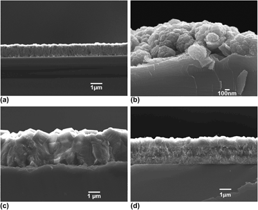
Single and multilayer diamond films were grown on silicon by varying substrate distance in hot-filament chemical vapor deposition. The grown films were characterized by scanning electron microscope (SEM) and Raman spectroscopy. From SEM surface images, it was observed that the films grown at substrate distances of 8, 7, and 6 mm and temperatures of 740, 780, and 830 °C possessed cauliflower, pseudocubes, and finally well-faceted cubes morphology. SEM fracture cross-sectional investigations revealed that growth of pseudocubes initiated on the top of cauliflower structure. By using the parametric relations gathered from single layer diamond growth studies, first time, multilayer diamond coatings were grown in situ with tunable thickness by only varying the substrate distance from filament assembly during deposition.

Type
Articles
Copyright
Copyright © Materials Research Society 2012

Access options

Get access to the full version of this content by using one of the access options below. (Log in options will check for institutional or personal access. Content may require purchase if you do not have access.)

References

REFERENCES

Angus, J.C. and Hayman, C.C.: Low-pressure, metastable growth of diamond and “diamondlike” phases. Science 241, 913921 (1988).CrossRefGoogle ScholarPubMed
Miyoshi, K., Wu, R.L.C., and Garscadden, A.: Friction and wear of diamond and diamondlike carbon coatings. Surf. Coat. Technol. 54/55, 428434 (1992).CrossRefGoogle Scholar
Nemanich, R.J., Baumann, P.K., Benjamin, M.C., Nam, O.H., Sowers, A.T., Ward, B.L., Ade, H., and Davis, R.F.: Electron emission properties of crystalline diamond and III-nitride surfaces. Appl. Surf. Sci. 130132, 694703 (1998).CrossRefGoogle Scholar
Geis, M.W., Efremow, N.N., Krohn, K.E., Twichell, J.C., Lyszczarz, T.M., Kalish, R., Greer, J.A., and Tabat, M.D.: A new surface electron-emission mechanism in diamond cathodes. Nature 393, 431 (1998).CrossRefGoogle Scholar
Sein, H., Ahmed, W., Jackson, M., Ali, N., and Gracio, J.: Stress distribution in diamond films grown on cemented WC–Co dental burs using modified hot-filament CVD. Surf. Eng. Technol. 163164, 196202 (2003).Google Scholar
Salgueiredo, E., Almeida, F.A., Amaral, M., Fernandes, A.J.S., Costa, F.M., Silva, R.F., and Oliveira, F.J.: CVD micro/nanocrystalline diamond (MCD/NCD) bilayer coated odontological drill bits. Diamond Relat. Mater. 18, 264270 (2009).CrossRefGoogle Scholar
Zhang, J., Zimmer, J.W., Howe, R.T., and Maboudian, R.: Characterization of boron-doped micro- and nanocrystalline diamond films deposited by wafer-scale hot filament chemical vapor deposition for MEMS applications. Diamond Relat. Mater. 17, 2328 (2008).CrossRefGoogle Scholar
Porro, S., Temmerman, G.D., Lisgo, S., John, P., Villalpando, L., Zimmer, J.W., Johnson, B., and Wilson, J.I.B.: Nanocrystalline diamond coating of fusion plasma facing components. Diamond Relat. Mater. 18, 740744 (2009).CrossRefGoogle Scholar
Haubner, R. and Lux, B.: Deposition of ballas diamond and nano-crystalline diamond. Int. J. Refract. Met. Hard Mater. 20, 93100 (2002).CrossRefGoogle Scholar
Köpf, A., Haubner, R., and Lux, B.: Multilayer coatings containing diamond and other hard materials on hardmetal substrates. Int. J. Refract. Met. Hard Mater. 20, 107113 (2002).CrossRefGoogle Scholar
Haubner, R. and Kalss, W.: Diamond deposition on hard metal substrates – comparison of substrate pre-treatments and industrial applications. Int. J. Refract. Met. Hard Mater. 28, 475483 (2010).CrossRefGoogle Scholar
Das, D. and Singh, R.N.: A review of nucleation, growth and low temperature synthesis of diamond thin films. Int. Mater. Rev. 52, 2964 (2007).CrossRefGoogle Scholar
Lee, S.T., Lin, Z., and Jiang, X.: CVD diamond films: Nucleation and growth. Mater. Sci. Eng., R 25, 123154 (1999).CrossRefGoogle Scholar
Gicquel, A., Hassouni, K., Silva, F., and Achard, J.: CVD diamond films: From growth to applications. Curr. Appl. Phys. 1, 479496 (2001).CrossRefGoogle Scholar
Liu, H. and Dandy, D.S.: Studies on nucleation process in diamond CVD: An overview of recent developments. Diamond Relat. Mater. 4, 11731188 (1995).CrossRefGoogle Scholar
Schäfer, L., Höfer, M., and Kröger, R.: The versatility of hot-filament activated chemical vapor deposition. Thin Solid Films 515, 10171024 (2006).CrossRefGoogle Scholar
Takeuchi, S., Oda, S., and Murakawa, M.: Synthesis of multilayer diamond film and evaluation of its mechanical properties. Thin Solid Films 398399, 238243 (2001).CrossRefGoogle Scholar
Ali, M. and Qazi, I.A.: Effect of substrate temperature on hot filament chemical vapor deposition grown diamond films. Int. J. Surf. Sci. Eng. 6(3), 214230 (2012).CrossRefGoogle Scholar
Frenklach, M. and Wang, H.: Detailed surface and gas-phase chemical kinetics of diamond deposition. Phys. Rev. B 43, 15201545 (1991).CrossRefGoogle ScholarPubMed
Skokov, S., Weiner, B., and Frenklach, M.: Elementary reaction mechanism for growth of diamond (100) surfaces from methyl radicals. J. Phys. Chem. A 98, 70737082 (1994).Google Scholar
Ali, M. and Ürgen, M.: Surface morphology, growth rate and quality of diamond films synthesized in hot filament CVD system under various methane concentrations. Appl. Surf. Sci. 257, 84208426 (2011).CrossRefGoogle Scholar
Clausing, R.E., Heatherly, L., Specht, E.D., More, K.L., and Begun, G.M.: Growth mechanism, film morphology, texture and stresses for three types of HFCVD diamond film growth. Carbon 28(6), 762763 (1990).CrossRefGoogle Scholar
Chen, Q., Yang, J., and Lin, Z.: Synthesis of oriented textured diamond films on silicon via hot filament chemical vapor deposition. Appl. Phys. Lett. 67, 18531855 (1995).CrossRefGoogle Scholar
Zhang, X., Shi, T., Wang, J., and Zhang, X.: Oriented growth of a diamond film on Si(100) by hot filament chemical vapor deposition. J. Cryst. Growth 155, 6669 (1995).CrossRefGoogle Scholar
Yu, Z. and Flodström, A.: Pressure dependence of growth mode of HFCVD diamond. Diamond Relat. Mater. 6, 8184 (1997).CrossRefGoogle Scholar
Huang, J.T., Yeh, W.Y., Hwang, J., and Chang, H.: Bias enhanced nucleation and bias textured growth of diamond on silicon (100) in hot filament chemical vapor deposition. Thin Solid Films 315, 3539 (1998).CrossRefGoogle Scholar
Taher, M.A., Schmidt, W.F., Naseem, H.A., Brown, W.D., Malshe, A.P., and Nasrazadani, S.: Effect of methane concentration on physical properties of diamond-coated cemented carbide tool inserts obtained by hot-filament chemical vapour deposition. J. Mater. Sci. 33, 173182 (1998).CrossRefGoogle Scholar
Shang, N., Fang, R., Liao, Y., and Cui, J.: Deposition of (100) and (110) textured diamond films on aluminum nitride ceramics via hot filament chemical vapor deposition. Jpn. J. Appl. Phys. 38, 15001502 (1999).CrossRefGoogle Scholar
Li, C-H., Liao, Y., Chang, C., Wang, G.Z., and Fang, R.C.: The nucleation and growth of (1 0 0)-textured diamond films in presence of nitrogen. Acta Phys. Sin. 49(9), 17561763 (2000).Google Scholar
Zhang, M., Gu, B., Wang, L., and Xia, Y.: X-ray detectors based on (100)-textured CVD diamond films. Phys. Lett. A 332, 320325 (2004).CrossRefGoogle Scholar
Zhang, M., Gu, B., Wang, L., and Xia, Y.: Preparation and characterization of (1 0 0)-textured diamond films obtained by hot filament CVD. Vacuum 79, 8489 (2005).CrossRefGoogle Scholar
Ma, Y., Wang, L.J., Liu, J.M., Su, Q.F., Xu, R., Peng, H.Y., Shi, W.M., and Xia, Y.B.: Characterization of (1 00)-orientated diamond film grown by HFCVD method with a positive DC bias voltage. Trans. Nonferrous Met. Soc. China 16, S313S316 (2006).CrossRefGoogle Scholar
Liao, Y., Chang, C., Li, C.H., Ye, Z.Y., Wang, G.Z., and Fang, R.C.: Two-step growth of high quality diamond films. Thin Solid Films 368, 303306 (2000).CrossRefGoogle Scholar
Li, X., Hayashi, Y., and Nishino, S.: An improved method for large-area oriented nucleation of diamond during bias process via hot-filament chemical vapor deposition. Thin Solid Films 308309, 163167 (1997).CrossRefGoogle Scholar
Wild, C., Kohl, R., Herres, N., Müller-Sebert, W., and Koidl, P.: Oriented CVD diamond films: Twin formation, structure and morphology. Diamond Relat. Mater. 3, 373381 (1994).CrossRefGoogle Scholar
Heimann, B., Raiko, V., and Buck, V.: Search for scaling parameters for growth rate and purity of hot-filament CVD diamond. Int. J. Refract. Met. Hard Mater. 19, 169175 (2001).CrossRefGoogle Scholar
Yarbrough, W.A., Tankala, K., Mecray, M., and DebRoy, T.: Hydrogen assisted heat transfer during diamond growth using carbon and tantalum filaments. Appt. Phys. Lett. 60, 20682070 (1992).CrossRefGoogle Scholar
Cheesman, A., Harvey, J.N., and Ashfold, M.N.R.: Studies of carbon incorporation on the diamond {100} surface during chemical vapor deposition using density functional theory. J. Phys. Chem. A 112, 1143611448 (2008).CrossRefGoogle ScholarPubMed
Singh, J.: Nucleation and growth mechanism of diamond during hot-filament chemical vapor deposition. J. Mater. Sci. 29, 27612766 (1994).CrossRefGoogle Scholar
LeGrice, Y.M., Nemanich, R.J., Glass, J.T., Lee, Y.H., Rudder, R.A., and Markunas, R.J.: Domain size determination in diamond thin films, in Diamond, Silicon Carbide and Related Wide Bandgap Semiconductors, edited by Glass, J.T., Messier, R., and Fujimori, N. (Mater. Res. Soc. Symp. Proc. 162, Pittsburgh, PA, 1990) pp. 219224.Google Scholar
Kuo, C.T., Lin, C.R., and Lien, M.L.: Origins of the residual stress in CVD diamond films. Thin Solid Films 290291, 254259 (1996).CrossRefGoogle Scholar
Prawer, S., Nugent, K.W., Jamieson, D.N., Orwa, J.O., Bursill, L.A., and Peng, J.L.: The Raman spectrum of nanocrystalline diamond. Chem. Phys. Lett. 332, 9397 (2000).CrossRefGoogle Scholar
Chattopadhyay, A., Sarangi, S.K., and Chattopadhyay, A.K.: Effect of negative dc substrate bias on morphology and adhesion of diamond coating synthesized on carbide turning tools by modified HFCVD method. Appl. Surf. Sci. 255, 16611671 (2008).CrossRefGoogle Scholar
Amaral, M., Almeida, F., Fernandes, A.J.S., Costa, F.M., Oliveira, F.J., and Silva, R.F.: The role of surface activation prior to seeding on CVD diamond adhesion. Surf. Coat. Technol. 204, 35853591 (2010).CrossRefGoogle Scholar