


Introduction
Thin films, even when made out of the most ductile metals, exhibit an extremely low fracture toughness compared with their bulk counterparts [Reference Wang, Kang, Zhang and Qin1, Reference Hirakata, Takeda, Kondo and Minoshima2, Reference Hosokawa, Desai and Haque3, Reference Hirakata, Nishijima, Fukuhara, Kondo, Yonezu and Minoshima4, Reference Kondo, Hiramine, Hirakata and Minoshima5]. As an example, the fracture toughness of 200-nm-thick gold membranes was measured to be only ∼2 MPa m1/2 [Reference Preiß, Gannott, Göken and Merle6], far off from the 50–100 MPa m1/2 reported in the literature for standard bulk specimens [7]. The scaling relationship between thickness and fracture toughness of thin films has already been investigated in detail in [Reference Wang, Kang, Zhang and Qin1, Reference Hirakata, Takeda, Kondo and Minoshima2, Reference Hosokawa, Desai and Haque3, Reference Hirakata, Nishijima, Fukuhara, Kondo, Yonezu and Minoshima4, Reference Pardoen, Hachez, Marchioni, Blyth and Atkins8, Reference Bluhm9]. The focus of the present study is, therefore, on identifying additional factors contributing to the low toughness of thin metallic films. A preliminary study [Reference Preiß, Merle and Göken10] evidenced that this low toughness is connected to the strong confinement of the plastic deformation in front of the notch, which strongly limits the energy dissipation during crack initiation and propagation. It was also observed that crack growth in polycrystalline thin films is usually intercrystalline [Reference Hirakata, Takeda, Kondo and Minoshima2, Reference Preiß, Merle and Göken10]. This second observation, consistent with previous reports in the literature [Reference Vayrette, Galceran, Coulombier, Godet, Raskin and Pardoen11, Reference Ast, Ghidelli, Durst, Göken, Sebastiani and Korsunsky12, Reference Pineau, Benzerga and Pardoen13, Reference Dugdale, Armstrong, Tarleton, Roberts and Lozano-Perez14, Reference Hosseinian, Gupta, Pierron and Legros15], suggests that grain boundaries (GBs) are easy crack propagation paths, as expected from the lower energy required to produce surfaces compared with an intracrystalline crack [Reference Sutton and Balluffi16]. In a semi-brittle or ductile metal, the resistance of a specific GB to crack propagation depends—in addition to the GB energy—on the relative orientation to the GB plane and crack propagation direction of the slip systems in the two grains [Reference Wang and Anderson17, Reference Kupka, Huber and Lilleodden18, Reference Möller and Bitzek19]. Atomistic simulations have recently also highlighted the importance of the local GB structure on fracture toughness [Reference Preiß, Gannott, Göken and Merle6]. Based on such reasoning and observations, GBs are generally seen as detrimental to the fracture toughness of thin films. To experimentally validate—or disprove—this assumption, we are comparing the fracture behavior of polycrystalline films to their single-crystalline counterparts. Silver was selected as a suitable model material for this purpose because of the availability of microfabrication techniques for preparing membranes with both microstructures (see Materials and methods section). The (100) single-crystalline and polycrystalline silver samples were subsequently subjected to plane-strain bulge testing, which is one of the few established methods for measuring the fracture toughness of thin films [Reference Preiß, Gannott, Göken and Merle6, Reference Preiß, Merle and Göken10, Reference Liddle, Huggins, Mulgrew, Harriott, Wade and Bolan20, Reference Merle and Göken21, Reference Xiang, McKinnell, Ang and Vlassak22, Reference Jaddi, Coulombier, Raskin and Pardoen23]. In parallel, atomistic simulations were performed to complement the experimental measurements and achieve a deeper insight into the failure mechanisms of the samples.
Results
Fracture toughness measurements
The bulge test experiments were performed on both notched (notch orientation: [110]) and un-notched thin film specimens of ∼200 nm thickness. Representative stress–strain curves for the polycrystalline and (100) single-crystalline specimens are shown in Fig. 1. In line with expectations, the polycrystalline (un-notched) specimens exhibit a considerably higher strength than the single-crystalline (un-notched) films, even though their initial (residual) stress is lower. The fact that all notched specimens failed at a significantly lower strain than their un-notched counterparts gives confidence in the validity of the fracture testing setup. The fracture toughness data were evaluated by Eq. (2), and are summarized in Table I.
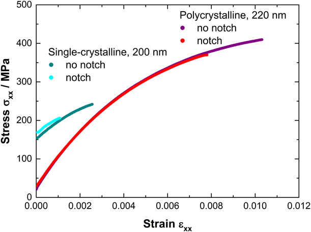
Figure 1: Stress–strain curves of polycrystalline and (100) single-crystalline silver membranes with and without notch. Please refer to the materials and methods section for experimental details.
TABLE I: Average, minimum, and maximum fracture toughness K IC for single-crystalline 200-nm-thick and polycrystalline 220-nm-thick silver membranes. Five samples were tested in each case.

The larger scattering in single-crystalline data can be attributed to the occasional presence of pit defects in the membranes. Nonetheless, there is no denying that the fracture toughness of the single-crystalline specimens is significantly lower than for their polycrystalline counterparts, which is itself only a small fraction of the tabulated macroscopic value (50–100 MPa m1/2 [7]).
Observation of crack propagation
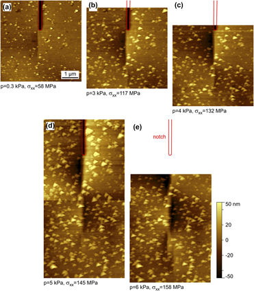
To understand the fracture behavior of single crystalline films, a 200-nm-thick silver film with a 20-µm long notch was tested in situ in the atomic force microscope (AFM). The membrane was loaded in pressure steps of 1 kPa until it failed at 7 kPa. Figure 2 shows a series of five AFM micrographs of the region in front of the notch tip. The position of the notch is highlighted by a red contour in all five scans. The small triangular features in the scans should be ignored: they are artifacts corresponding to the self-imaging of the AFM tip on contaminants present on the surface of the membrane. Noteworthy are the straight lines appearing on the micrographs, which correspond to height steps. Already at the initial pressure of 0.3 kPa (scan a), a 1.6-µm long straight line parallel to the notch originates from its tip. At a pressure of 3 kPa (scan b), an additional shorter line with weaker contrast appears ahead of the first line, albeit with a small lateral offset, which brings it back in line with the notch. The height of the initial step also increased, as can be seen from the increasing color contrast. These events are basically repeated upon the following pressurizations so that height steps are ultimately spread over a distance of almost 10 µm in front of the notch tip [Fig. 2(e)], before the sample suddenly fails. There is a strong suggestion that the formation of height steps eases crack propagation by providing a path of weaker resistance.

Figure 2: Atomic force microscopy (AFM) scans collected during an in situ fracture bulge test of a 200-nm-thick single-crystalline silver film. The pressure and the stress increase from (a) to (e) is indicated below each scan. The scans were vertically aligned to each other and the notch tip is indicated as a red contour. The small triangular features are imaging artifacts that should be overlooked.
These height steps were, therefore, investigated more closely by electron backscatter diffraction (EBSD) on a sample that had only experienced very little pressurization so that it did not fail. The EBSD mapping shown in Fig. 3 reveals that the height step corresponds to the formation of a twin domain in front of the notch. This is consistent with the surface inclination of 9°–19° measured by AFM, which suits quite well the 12.3° slope expected for the formation of a Σ3 coherent twin boundary, as schematically shown in Fig. 4.
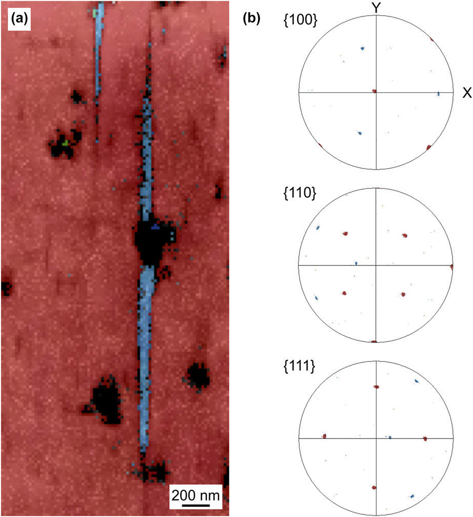
Figure 3: EBSD crystal orientation mapping (a) of the area in front of the notch tip in a deformed 200 nm-thick single-crystalline silver film. Σ3 twin boundaries are found between the domains. (b) Corresponding pole figures, using the same color code.
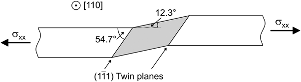
Figure 4: Schematics of the cross-section of a single-crystalline (001) Ag film containing a twin ahead of the crack notch.
The periodic switching of the slope of the steps visible in Fig. 2 is quite reminiscent of the flip-flop failure mechanism evidenced in symmetrically loaded large plates [Reference El-Naaman and Nielsen24, Reference Nielsen and Hutchinson25]. However, the Ag thin films exhibit a new form of this behavior, with an alternation in crystallographic twinning planes replacing the alternation of ductile slant failure zones of opposite slopes found in thicker plates.
In any case, as the transition from the dislocation-based plasticity prevalent in polycrystalline samples [Reference Preiß, Merle and Göken10] to twinning in front of the notch tip in the single-crystalline seems to be pivotal to the fracture behavior of the films, its origins were investigated more thoroughly by a modeling approach.
Atomistic simulations
Figure 5 shows snapshots of the initial deformation mechanisms of a 12-nm-thick single-crystalline Ag thin film with crystal and notch orientation identical to the experimental setup. To characterize the dislocation processes during the deformation at constant uniaxial strain rate, the Thompson tetrahedron notation [Reference Hirth and Lothe26] is employed. At a strain of ε = 1.6%, the first partial dislocation αB(a) was nucleated from the intersection between one notch tip and the bottom surface, see Fig. 5(a). This dislocation produced a stacking fault in its wake, which extended through the height of the thin film. Further partial dislocations αB(a) were nucleated on parallel (a) planes from similar positions. At the other notch tip, a partial dislocation βA(b) was also first nucleated from the bottom surface. Then, a partial dislocation with identical Burgers vector was nucleated on the adjacent (b) plane, forming a micro twin, see Fig. 5(c). Meanwhile, at ε = 1.8%, a dislocation αB(a) was also nucleated from the top surface of the notch tip, see Fig. 5(c). This partial dislocation intersected the micro-twin and left stair-rod dislocation segments at its boundaries. On the other side of the slit, where the partial dislocations had been nucleated on parallel (a) planes, parallel micro twins formed in a similar process, see Fig. 5(c). These micro twins finally coalesced in a large twin, see Fig. 5(e). On the other side, a micro twin formed from the partial dislocation βA(b). This micro twin effectively hindered the further propagation of the larger twin segment, leading to necking, see Fig. 5(f).
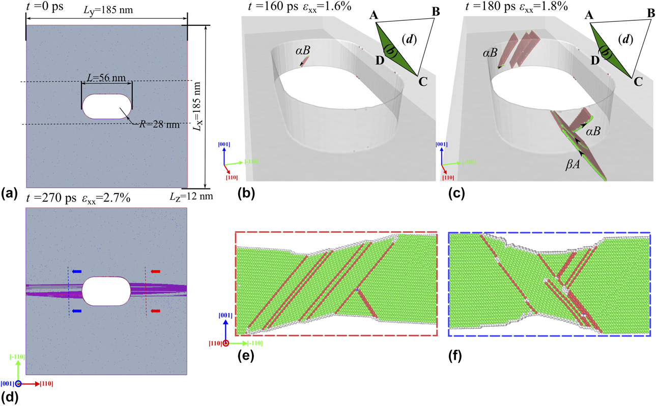
Figure 5: Atomistic simulations showing different deformation stages: (a) Initial sample. (b) Nucleation of the first leading partial dislocation. (c) Nucleation of another leading partial dislocation and formation of a micro-twin. Black arrows denote the line direction. (d) Deformed sample. (e) Cross-section showing twins forming on the right side of the slit. (f) Cross-section showing necking on the left side of the slit. For (a and d), the color denotes the coordination number. 8: gray; 9: magenta; and 11: violet red. For (b), (c), (e), and (f), green atoms are identified as undisturbed FCC structure, red atoms represent stacking faults, and gray atoms correspond to other defects.
Discussion
Twinning behavior
The bulge experiments on the 200-nm-thick single-crystalline Ag specimens as well as the atomistic simulations on the about 16-time thinner samples suggest that the initial deformation of the Ag(001) single-crystalline films with slits along [110] the direction is governed by the nucleation of micro twins instead of full dislocations. The behavior of dislocations around a crack tip can be rationalized by calculating the resolved shear stresses acting on the different slip systems from the anisotropic elastic solution for the stress field of a mode I loaded sharp crack [Reference Liebowitz and Sih27]. For the given orientation, these driving forces were already calculated for an fcc system by Bitzek and Gumbsch [Reference Bitzek and Gumbsch28]. Dislocations on the oblique  $\left( {\bar{1}1\bar{1}} \right)$ and $\left( {1\bar{1}\bar{1}} \right)$ planes with Burgers vector orientations [011], $\left[ {\bar{1}01} \right]$, $\left[ {01\bar{1}} \right]$ and $\left[ {\bar{1}0\bar{1}} \right]$ [DB(a), CB(a), AC(b) and AD(b) in Thompson tetrahedron notation] were shown to experience the highest driving forces [Reference Bitzek and Gumbsch28]. This is in agreement with slip on these planes observed in the experiments and simulations. To understand why twinning rather than full dislocation activity was observed on these planes, the resolved shear stresses on the leading and trailing partial dislocations αB(a) and Dα(a) as well as on the full dislocation DB(a) were calculated and are shown in Figs. 6(a)–6(c). These dislocations are representative of the most highly stressed class of dislocations. The results for the other aforementioned slip systems would be qualitatively and quantitatively identical, with the stress field being mirrored at the crack plane in some cases [Reference Bitzek and Gumbsch28]. As can be seen in Fig. 6(a), the leading partial dislocation αB(a) experiences a large resolved shear stress in the entire region ahead of the crack tip. In contrast, the trailing partial dislocation Dα(a) experiences a change in sign in the region ahead of the crack tip, see Fig. 6(b); i.e., while some parts of the trailing dislocation are repelled from the crack tip, other parts are actually attracted toward the crack tip. The nucleation of a trailing dislocation from the crack tip is, therefore, hindered. However, the full dislocation DB(a) experiences no such drastic change in driving force, see Fig. 6(c). The question then arises: under which conditions are only leading partial dislocations nucleated and when should full dislocations be expected?
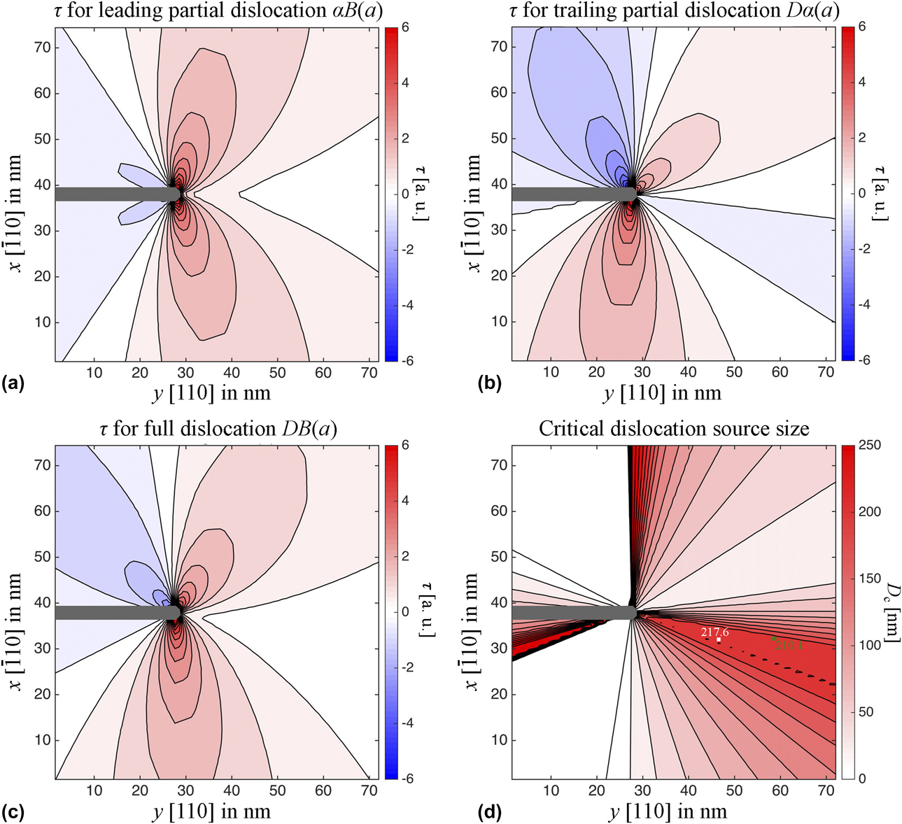
Figure 6: (a–c) Resolved shear stress on (a) the leading partial dislocation; (b) the trailing partial dislocation; and (c) the corresponding full dislocation for a representative dislocation of the most highly stressed slip systems. The values were calculated from the anisotropic elastic solution for the stress tensor around a sharp crack in Ag, using an arbitrary stress intensity factor K I. (d) Shows for this case the critical dislocation source size as estimated by Eq. (1).
It is well known from small-scale investigations that in dislocation nucleation–controlled plasticity, the deformation mode—namely, full dislocation slip versus partial dislocations and twinning-mediated deformation—is related to the crystallite size [Reference Chen, Ma, Hemker, Sheng, Wang and Cheng29, Reference Sedlmayr, Bitzek, Gianola, Richter, Mönig and Kraft30, Reference Kraft, Gruber, Mönig and Weygand31]. Following the approach of Chen et al. [Reference Chen, Ma, Hemker, Sheng, Wang and Cheng29], one can compare the resolved shear stress necessary to generate a full dislocation with Burgers vector b f with the one necessary to form only the leading partial dislocation (Burgers vector b lp) plus the stacking fault (with stacking fault energy γsf) from a source of size D. From that, one can determine the critical source size D c below which the stress to nucleate a leading partial dislocation becomes smaller than the stress to nucleate a full dislocation [Reference Chen, Ma, Hemker, Sheng, Wang and Cheng29]. This is a necessary condition for the plastic deformation of a dislocation-free crystal by the nucleation and propagation of twins. Bitzek et al. [Reference Sedlmayr, Bitzek, Gianola, Richter, Mönig and Kraft30, Reference Bitzek32] adapted this twinning criterion to single crystals under uniaxial deformation. It can, however, be further generalized to arbitrary stress states in single crystals by calculating the resolved shear stress τ = (σ·n)·b/|b| for the full (τf) and leading partial dislocation (τlp) from the (locally varying) stress tensor σ [Reference Hirth and Lothe26]. The critical source size then becomes:
 $${D_{\rm{c}}} = {{2\alpha \mu } \over {{\gamma _{{\rm{SF}}}}}}\left( {{{{\tau _{{\rm{lp}}}}} \over {{\tau _{\rm{f}}}}}{b_{{\rm{lp}}}}{b_{\rm{f}}} - b_{{\rm{lp}}}^2} \right)\quad ,$$
where α is a parameter dependent on the character of the dislocation (α = 0.5 and 1.5 for edge and screw dislocations, respectively) [Reference Chen, Ma, Hemker, Sheng, Wang and Cheng29]. The critical source size, Eq. (1), was estimated for b f = DB and b lp = αB gliding on the (a) plane  $\left( {{\rm{normal}}\;{\rm{vector}}\;{\bi{n}} = {{\left[ {\bar{1}1\bar{1}} \right]} / {\sqrt 3 }}} \right)$. The corresponding map of the critical source size is shown in Fig. 6(d), taking α = 1 [Reference Chen, Ma, Hemker, Sheng, Wang and Cheng29] and using the parameters for Ag from [Reference Williams, Mishin and Hamilton33] to calculate the anisotropic elastic stress field around a semi-infinite crack in an infinite medium for an arbitrary value of stress intensity factor K I [Reference Liebowitz and Sih27]. In a dislocation-free film, the dislocations need to be generated from the crack tip. In this case, the effective dislocation source lies at the intersection of the glide plane and the notch. Only the region ahead of the crack tip is relevant, as dislocations emitted backward would not contribute to an unloading of the crack. In order for a dislocation to form and be emitted from the crack, it should experience a positive driving force throughout the film thickness. The (a) plane is inclined with respect to the film thickness. On this glide plane, the shortest possible straight dislocation line spanning the entire film thickness will be exposed to the stress variation ahead of the crack plotted along the y-axis in Fig. 6. Therefore, the largest D c ahead of the crack will determine whether a partial or a full dislocation is formed. According to Fig. 6(d), this would be D c ≈ 200 nm. The dislocation source must, however, be smaller than the film thickness. Assuming a maximal source size of about half the film thickness, the critical thickness for the emission of a full dislocation from the crack tip should be larger than about 400 nm. In this orientation, twinning is, therefore, expected to be the dominant deformation mechanism in the 200-nm thin films, as evidenced in the bulge test experiments.
This approach can obviously only provide a rough estimate for the critical film thickness at which the transition from twinning to full dislocation slip should occur, as the scaling of dislocation source length with the film thickness as well as the source configurations are not known. Furthermore, effects such as the creation of surface steps are neglected and the stress field around blunt notches will differ from the analytical stress field of sharp cracks. Nevertheless, this approach can be useful to compare different crack orientations and materials. For instance, for notched (001) copper films in [110] loading direction, as studied by Hirakata et al. [Reference Hirakata, Yoshida, Kondo and Minoshima34], one would expect the critical thickness to be reduced by a factor of approximately two, compared with silver (using the materials parameters for Cu from [Reference Mishin, Mehl, Papaconstantopoulos, Voter and Kress35]). This is consistent with the 2- to 3- time larger stacking fault energy of Cu [Reference Liebig, Krauß, Göken and Merle36] compared with Ag [Reference Williams, Mishin and Hamilton33] and in agreement with the experimental observation of full dislocations in ∼300-nm thin films by Hirakata et al. [Reference Hirakata, Yoshida, Kondo and Minoshima34].
Fracture toughness
While the origins of the twinning deformation behavior of the single-crystalline films are now better understood, the question remains how this deformation mechanism can account for the fracture toughness being 40% lower than for their polycrystalline thin film counterparts. Actually, the toughness measured on single-crystalline specimens is only slightly higher than the lower bound of 0.45 MPa m1/2 according to the Griffith theory, that takes into account only the formation of free surfaces (based on a surface energy of 1.22 J/m2 for silver [Reference Tyson and Miller37]). The general validity of this trend is supported by a study by Hirakata et al. on copper thin films, which also reports significantly lower fracture toughness values for single-crystalline films (loaded in both [110] and [100] direction) than for polycrystalline ones [Reference Hirakata, Yoshida, Kondo and Minoshima34]. Interestingly, this trend holds true for specimens above the thickness threshold for full dislocation nucleation, as well as for specimens with pre-existing dislocations close to the notch tip, in which case, plasticity is not nucleation-controlled. For such specimens, Hirakata et al. [Reference Hirakata, Yoshida, Kondo and Minoshima34] observed similar mechanisms of chisel point fracture in both single-crystalline and polycrystalline films. In this case, the difference in fracture toughness is more likely a consequence of a large difference in the respective yield strengths of the specimens, which was previously reported to scale with the fracture toughness in metallic thin films [Reference Preiß, Gannott, Göken and Merle6].
Although their low strength might also contribute to the low fracture toughness of the thin single-crystalline Ag specimens investigated in this study, the AFM micrographs acquired during in situ testing point at the initiation of twinning being the main cause. Because of twinning, a surface step of up to 80 nm height (compare with the total film thickness of 200 nm) was observed before fracture took place, see Fig. 2. This step results in the formation of two kinks of locally thinner cross-section, which also act as stress concentrators. The ragged appearance of the breaking edges of an arrested crack, shown in Fig. 7, suggests that final fracture involves the formation of micro cracks or voids along these kinks, with progressive coalescence. This suggests an interplay of deformation mechanisms different from pure twinning, which is also supported by our atomistic simulation results showing additional necking through, intersecting twins. Similarly, TEM observations by Pashley and Oh et al. showed slip of both full and partial dislocations to be involved in the final deformation stages before fracture in single-crystalline gold films of both (100) and (111) orientations [Reference Pashley38, Reference Oh, Legros, Kiener, Gruber and Dehm39].
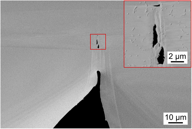
Figure 7: Electron micrograph showing an arrested crack in a 400-nm-thick single-crystalline silver film. Similar to the 200-nm-thick films, voids and cracks are nucleated along the twin steps. However, because of the larger film thickness, the crack nucleation and propagation is retarded.
Because of a limited number of specimens, no in situ tests could be performed on the polycrystalline silver films in the AFM. Nonetheless, it is very likely that they would exhibit a similar crack growth behavior as already reported in detail for polycrystalline gold films of similar microstructure [Reference Preiß, Merle and Göken10]. For both single-crystalline and polycrystalline specimens, a narrow fracture process zone develops ahead of the notch. In the polycrystalline gold case, it was shown that its width is confined by the film thickness because of the initiation of necking [Reference Preiß, Merle and Göken10], which originated from the out-of-plane plastic deformation mediated by dislocations or GBs. In the polycrystalline silver films, twinning might play a more important role than in gold because of the lower stacking fault energy. However, the development of the twins is geometrically limited by the (very small) grain dimension, and not all grains are favorably oriented for twinning, thus making little difference from dislocation-mediated plastic deformation. Twinning is comparatively unconstrained in the single-crystalline specimens so that a stronger local reduction in the effective (projected) thickness will occur at a lower stress level. Furthermore, subsequent twin growth is eased, as it requires only very low stresses, and is less hampered by strain hardening than in a polycrystalline film, as confirmed by the stress–strain curves presented in Fig. 1. This—together with the more effective thickness reduction by twinning—is the likely reason for the significantly lower fracture toughness of the single-crystalline films. Another reason is that the crack formation and propagation is straight in the single-crystalline samples, while it mostly follows pre-existing GBs in the polycrystalline case [Reference Preiß, Merle and Göken10]. Such a meandering propagation is known to increase the effective fracture toughness of the specimens [Reference Sutton and Balluffi16]. Granted, this increase is somehow counterbalanced by the lower toughness of GBs, compared with the lattice of a single crystal. However, a simple consideration of the ratio between free energy of common GBs and surface energy evidences that the latter effect is minimal. For instance, the value of 0.21 J/m2 reported by Barg et al. for an incoherent Σ3 grain boundary [Reference Barg, Rabkin and Gust40]—which should fall close to the energy of most large angle GBs—amounts for less than 9% of the energy required to form two free surfaces from the bulk [Reference Tyson and Miller37] so that the toughness should only be marginally lower. Furthermore, intercrystalline crack growth is preceded by plastic dissipation inside a small but not negligible fracture process zone, which increases the overall energy consumption compared with the sole bond-breaking fracture process. It is, therefore, likely that crack meandering and GBs, in general, have a strong positive net effect on the fracture toughness of the polycrystalline samples.
Conclusions
Bulge tests revealed that the fracture toughness of 200-nm thin single-crystalline silver films with (001) surfaces and notches along [110] is even lower than that of their polycrystalline counterparts and barely exceeds the energy required for the creation of free surfaces. This was mostly accounted for by the transition to a different deformation mechanism than classical full dislocation plasticity at the notch tip, which consisted in the nucleation, extension, and intersection of twins. By deriving a generalized, size- and orientation-dependent twinning criterion, it was shown that for single-crystalline silver films with this crystal orientation, twinning is expected to be the dominant mechanism of crack tip plasticity for film thicknesses less than approximately 400 nm. Atomistic simulations furthermore suggest that intersecting twins significantly contribute to localized necking and failure. In such a single-crystalline specimen, twins emitted from the notch tip create a straight path where the stress is magnified, which promotes the extension of the crack. In comparison, the GBs of the polycrystalline samples provide a meandering path for the crack to propagate, which extends the effective crack length and increases the fracture toughness of these specimens. Owing to the occurrence of full dislocation plasticity in the polycrystalline films, the crack extension is preceded by the formation of a small plastic fracture process zone, which also contributes to an overall tougher behavior than for single-crystalline films.
Materials and methods
Samples
Single-crystalline silver films
The single-crystalline films were produced by heteroepitaxial growth onto a sacrificial 10-µm-thick Si(100) membrane held inside a thicker 4 × 1-mm Si frame, produced by Nanoworld GmbH (Erlangen, Germany). Combining silver with silicon might appear paradoxical, as their lattice misfit is very high (33%). Nevertheless, epitaxial growth of silver on Si(100) has often been observed under moderate to high sputtering deposition rates [Reference Hanawa and Oura41, Reference Hanbücken and Neddermeyer42, Reference Khare, Gerlach, Patzig and Rauschenbach43, Reference Nason, You and Lu44, Reference Je, Kang and Noh45, Reference Yang, Lambeth, Tang and Laughlin46]. This is usually ascribed to the fact that the length of three unit cells of silicon agrees well with that of four unit cells of silver [Reference Nason, You and Lu44, Reference Je, Kang and Noh45, Reference Yang, Lambeth, Tang and Laughlin46], leading to an Ag(100)//Si(100) orientation relationship with Ag〈110〉//Si〈110〉. The single-crystalline silver films were deposited using a magnetron sputtering system (DCA Instruments Oy, Turku, Finland) with a base pressure of 1 × 10⁻⁹ mbar. To remove contamination and to reduce potential defects at the silicon surface, the samples were first sputter-cleaned for 5 min at 200 eV and heated to 1000 °C for 1 h under ultra-high vacuum conditions. Silver was deposited to a thickness of 200 nm at a deposition rate of 7.6 Å/s, under an argon pressure of 2.8 × 10⁻³ mbar and a constant substrate temperature of 300 °C. The membranes were subsequently released by wet etching the sacrificial silicon substrate, yielding nine freestanding samples.
As expected from the literature, the epitaxial growth resulted in the surface normal of the film being aligned with the [001] crystal direction, whereas the long and short axis of the membrane match the  $\left[ {\bar{1}10} \right]$ and the [110] crystal directions, see Fig. 8(a). Consequently, the close-packed {111} planes are parallel to the membrane axes and cut the surface of the film at an angle of 54.74°. Electron channeling contrast imaging (ECCI) [Reference Zaefferer and Elhami47] evidenced the presence of a network of stacking faults running along the 〈110〉 directions, see Fig. 8(b). This is presumably a consequence of the aforementioned lattice constant mismatch between silicon and silver.
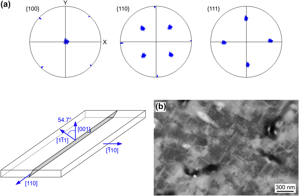
Figure 8: Single-crystalline silver thin films (200 nm thickness): (a) Pole figures showing the orientation of the crystallographic planes as obtained from a 50 × 85-µm2 EBSD mapping of a 200-nm-thick single-crystalline Ag film—(b) ECCI micrograph of a single-crystalline Ag film. The perpendicularly oriented straight features are stacking faults along the 〈110〉 directions of the film. An oxide layer was partially covering the surface at the time of imaging.
Polycrystalline silver films
One batch of polycrystalline silver films was prepared to serve as a reference. The films were obtained by thermal evaporation on a sacrificial 1 × 4-mm, 100-nm-thick SiNx substrate membrane (Silson Ltd., Southam, Warwickshire, U.K.), using a custom-built setup (see Refs. Reference Merle, Cassel and Göken48 and Reference Merle49 for details). The deposition was performed at a rate of 8 Å/s, while the substrate was heated at 85 °C and rotated at 10 rpm. These parameters were mainly selected because they yield a low sample surface roughness (R a < 4.5 nm).
The resulting microstructure corresponds to the T zone of the Grovenor model [Reference Grovenor, Hentzell and Smith50], see Fig. 9. From the plan view micrographs, a mean grain size of 110 nm is evidenced, which is only about half of the film thickness (220 nm). These polycrystalline samples were subsequently made freestanding by CF4 reactive ion etching (see Ref. Reference Preiß, Gannott, Göken and Merle6 for details).
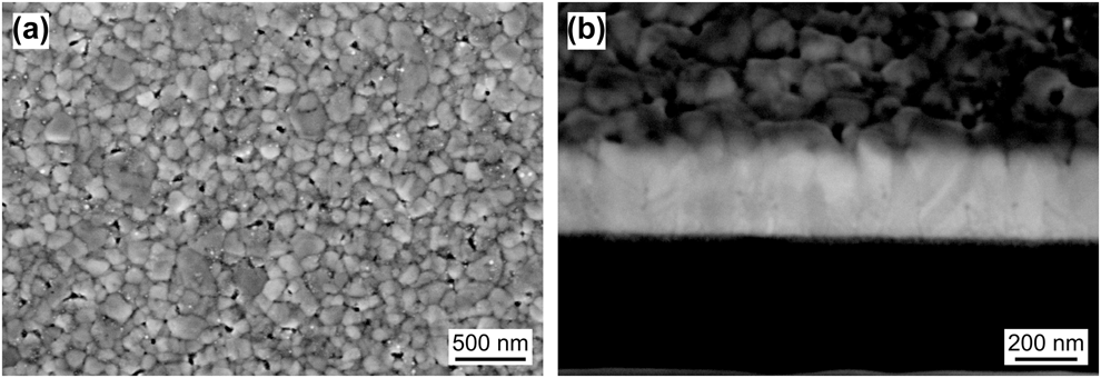
Figure 9: Electron micrograph of the 220-nm-thick polycrystalline Ag film (a) The average in-plane grain size is 110 nm. (b) Focused ion beam (FIB)–milled cross-section of the same film revealing mostly columnar grains with partly inclined GBs and some smaller grains on the bottom surface of the film. Some inclined twins can also be observed.
Bulge testing
The samples were mechanically tested using a custom-built bulge setup, which relies on gaseous nitrogen to pressurize the membranes (see description in Ref. Reference Merle49). To perform fracture testing, the same technique was used as in Ref. Reference Preiß, Merle and Göken10: a 10- to 20-µm long slit, with a notch radius of approximately 100 nm, was introduced at the center of each membrane by focused ion beam milling (Crossbeam 1540, Zeiss, Oberkochen, Germany), and the sample was subsequently pressurized until failure. Using the analytical model of Vlassak et al. [Reference Vlassak and Nix51], the long-range lateral stress present in the 1 × 4-mm membranes was derived from the experimental pressure-deflection data until final failure. As in Refs. Reference Preiß, Gannott, Göken and Merle6, Reference Preiß, Merle and Göken10, Reference Merle and Göken21, and Reference Xiang, McKinnell, Ang and Vlassak22, the fracture toughness K IC was calculated from the fracture stress σxx,fracture and the half length of the notch a notch using Irwin’s definition [Reference Irwin52]:
 $${K_{{\rm{IC}}}} = {\sigma _{xx{\rm{,fracture}}}}\sqrt {\pi {a_{{\rm{notch}}}}} \quad .$$
For selected specimens, the custom-built bulge tester was operated in situ in a Dimension 3100 AFM (Bruker Nano Analytics, Berlin, Germany), which allowed for the observation of the crack propagation. This operation mode is described in detail in Ref. Reference Preiß, Merle and Göken10.
Simulations
Atomistic simulations were performed using the embedded atom method (EAM) potential for silver developed by Mishin et al. [Reference Williams, Mishin and Hamilton33]. The relevant properties of this potential, which are also used in the determination of resolved shear stresses and critical source size, are b f = 0.29 nm, b lp = 0.17 nm, γSF = 17.8 mJ/m2, c 11 = 124.2 GPa, c 12 = 93.9 GPa, c 44 = 46.4 GPa, and μ = (c 11 − c 12 + c 44)/3 = 25.6 GPa.
The thin film was modeled as a rectangular cuboid of 185 × 185 nm side lengths and 12 nm height. It contained a central slit of 56 nm length and 28 nm width, with a tip radius of 14 nm, see Fig. 5(a). The setup was designed with the same crystallographic orientations as the single-crystalline specimens used in the experiments, with a slit parallel to the y = [110] direction. The surfaces in z direction were free, while 2D dynamic boundary conditions were used for atoms within 1.2 nm of the x and y boundaries of the cuboid. After relaxation by the FIRE algorithm [Reference Bitzek, Koskinen, Gähler, Moseler and Gumbsch53], the sample was scaled to the lattice constant a 0 = 0.41155 nm at 300 K and equilibrated at 300 K for 20 ps using the Nosé–Hoover thermostat and barostat to relieve stresses in the axial directions [Reference Hoover54]. Uniaxial tensile tests were performed in x direction at a constant strain rate of 108 s−1, while maintaining zero stress in the y direction and a constant temperature of 300 K. Dislocations were identified and visualized by the dislocation analysis (DXA) tool in OVITO [Reference Stukowski55].
Acknowledgments
The support from Thomas Sulzbach and Christoph Richter from Nanoworld Services GmbH Erlangen for structuring the silicon substrates is gratefully acknowledged. The authors would like to thank Ilse Lakemeyer from MPI Stuttgart for her dedicated support with the deposition of the films and Mark Wobrock for preliminary work at MPI related to SX-Ag deposition. L.H. thanks Zhuocheng Xie for helpful discussions. This research used resources from the ‘Center for Nanoanalysis and Electron Microscopy’ (CENEM) at FAU Erlangen. B.M., H.L., and M.G. also acknowledge financial support by the Deutsche Forschungsgemeinschaft (DFG) within the Cluster of Excellence “Engineering of Advanced Materials” (Project EXC 315, including Bridge Funding) and the research training group GRK1896 ‘In situ Microscopy with Electrons, X-rays and Scanning Probes’. E.B. gratefully acknowledges the funding from the European Research Council (ERC) under the European Union’s Horizon 2020 research and innovation program through the project “microKIc—Microscopic Origins of Fracture Toughness” (grant agreement No. 725483). Computing resources were provided by the Regionales RechenZentrum Erlangen (RRZE).


 Open access