


Introduction
Scanning electron microscopy (SEM) based systems are major inspection and metrology tools to measure critical dimensions (CDs) in nanofabrication because they provide optimal functionality by combining high-resolution with high-speed, and non-destructive imaging (Solecky et al., Reference Solecky, Rasafar, Cantone, Bunday, Vaid, Patterson, Stamper, Wu, Buengener, Weng and Dai2017; Orji et al., Reference Orji, Badaroglu, Barnes, Beitia, Bunday, Celano, Kline, Neisser, Obeng and Vladar2018). However, information from 3D samples reduces to a gray-scale value in SEM micrographs, where one cannot easily measure the structure height.
To obtain structure height, or a 3D map of the surface in general, combinations of tools and techniques are being employed such as stereo vision, structure from motion, or stereo-photogrammetry (Faber et al., Reference Faber, Martinez-Martinez, Mansilla, Ocelík and De Hosson2014; Eulitz & Reiss, Reference Eulitz and Reiss2015; Tafti et al., Reference Tafti, Kirkpatrick, Alavi, Owen and Yu2015; Shanklin, Reference Shanklin2016). In these methods, a sample is illuminated and/or viewed at different angles by introducing extra sources, detectors, and/or tilting the sample such that feature height is measured as a lateral distance, or at least can be calculated from the projection. However, this is not practical or even possible in many scenarios, especially in wafer-scale production (Frase et al., Reference Frase, Gnieser and Bosse2009). Furthermore, the accuracy of state-of-the-art commercial software packages is disputed in the literature (Marinello et al., Reference Marinello, Bariani, Savio, Horsewell and De Chiffre2008; Tondare et al., Reference Tondare, Villarrubia and Vladár2017). Although the aforementioned reconstruction methods have been in use for a few decades, height information embedded in top-down SEM images itself is not studied well enough. Extraction of the embedded information can improve the efficiency of available techniques and also lead to measuring the height directly from top-down (0° tilt angle) SEM images, which are already available for CD measurements.
In this work, we studied the relation between step height and the emission of secondary electrons (SEs) resulting from exposure with primary electrons (PEs) at different energies. The material of choice is silicon (Si). As visualized in Figure 1, the SE emission on the sidewall of the step depends on the PE energy and the step height. By using this phenomenon, we present a method to determine the height of structures from top-down SEM images.
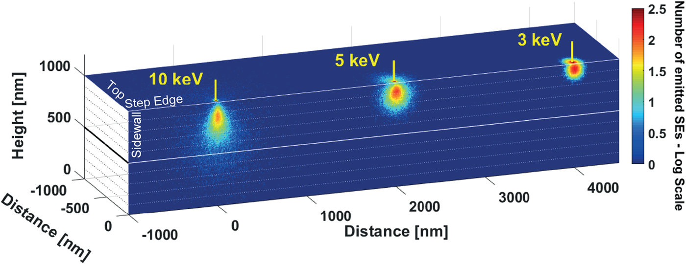
Fig. 1. SE emission sites on the top and the sidewall of a (1 µm high) step are shown for three acceleration voltages (10, 5, and 3 keV). The zero-diameter electron beam (with 104 electrons) lands on top of the step, 50 nm away from the edge. The white dashed lines on the sidewall aid in judging how many electrons can actually be emitted from a particular depth of the step.
Theory and Simulations
When a sample is exposed by using an electron probe, the size of the electron interaction volume inside the material is a function of material properties and beam energy. The number of electrons emitted from the sample is proportional to the intersection of the interaction volume and the sample surface.
Consider two step heights, formed by the sidewall of the Si step shown in Figure 1, one bounded by a horizontal plane (Si) at 200 nm depth from the top surface, and the other bounded by a plane (Si) at 500 nm depth. The cross-sections of these steps are illustrated in Figures 2a–2d.
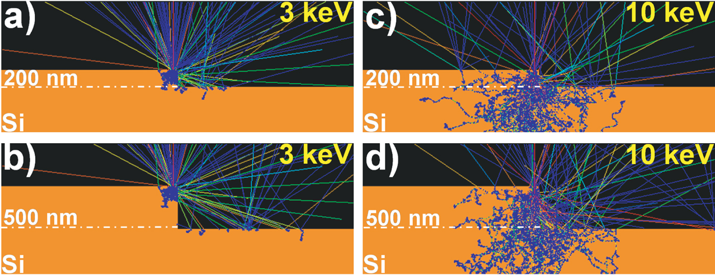
Fig. 2. Cross-sectional view of the interaction volume with respect to step height and beam energy. The horizontal FoV is 4 µm and a zero diameter beam is focused 50 nm left from the step edge.
At low energy (e.g., 3 keV as in Figs. 2a, 2b), electrons do not penetrate deeper than the height of the steps. Therefore, the same number of electrons will be emitted, even though the steps are different in height. In other words, at this beam energy the emission is insensitive to step height.
If the beam energy is increased, the interaction volume becomes larger and effectively shifts down. At a certain energy, some of the electrons penetrate deeper than the height of the smaller step and are buried in the sample. However, those electrons can still escape from the lower part of the sidewall of the higher step and contribute to the detected signal, as illustrated in Figures 2c and 2d.
The increase in the SE-signal intensity when scanning over an edge is a well-known phenomenon (topographic contrast) (Reimer, Reference Reimer1998), and frequently used to measure lateral sizes from SEM images, but its connection with the height, as described above, has not yet been exploited in a quantitative way. To establish this connection, we use Monte Carlo simulations.
A simulator, e-scatter* (Verduin et al., Reference Verduin, Lokhorst and Hagen2016) models the elastic scattering using Mott cross-sections for energies higher than 200 eV, including solid-state effects using a muffin-tin potential, as calculated using ELSEPA (Salvat et al., Reference Salvat, Jablonski and Powell2005). For energies lower than 100 eV, electron–phonon scattering is taken into account (Fitting et al., Reference Fitting, Schreiber, Kuhr and Von Czarnowski2001; Schreiber & Fitting, Reference Schreiber and Fitting2002). For energies in between, the scattering cross-sections of the two mechanisms are interpolated (Verduin, Reference Verduin2016). The inelastic scattering and the generation of SEs are based on dielectric function (Kieft & Bosch, Reference Kieft and Bosch2008). Boundary crossing is modeled based on momentum conservation and extended with the quantum mechanical transmission probability (Shimizu & Ze-Jun, Reference Shimizu and Ze-Jun1992). The simulator traces all electrons until they either reach the flat detector at the top of the sample or end up with energy too low to escape from the material. Moreover, the simulator runs on a graphics processing unit such that it benefits from massive parallelism (Verduin et al., Reference Verduin, Lokhorst and Hagen2016).
Now, we extend the analysis from single spot exposure mode, as shown in Figure 2, to line scan mode. Figure 3 compares the simulated line scans, using 20,000 electrons per 1 nm × 1 nm pixel (these are default values, unless stated otherwise) over the 200 and 500 nm steps shown in Figure 2. In Figure 3a the topographic contrast is clearly seen, but the SE-signal resulting from exposure with a 3 keV beam is the same for both step heights.
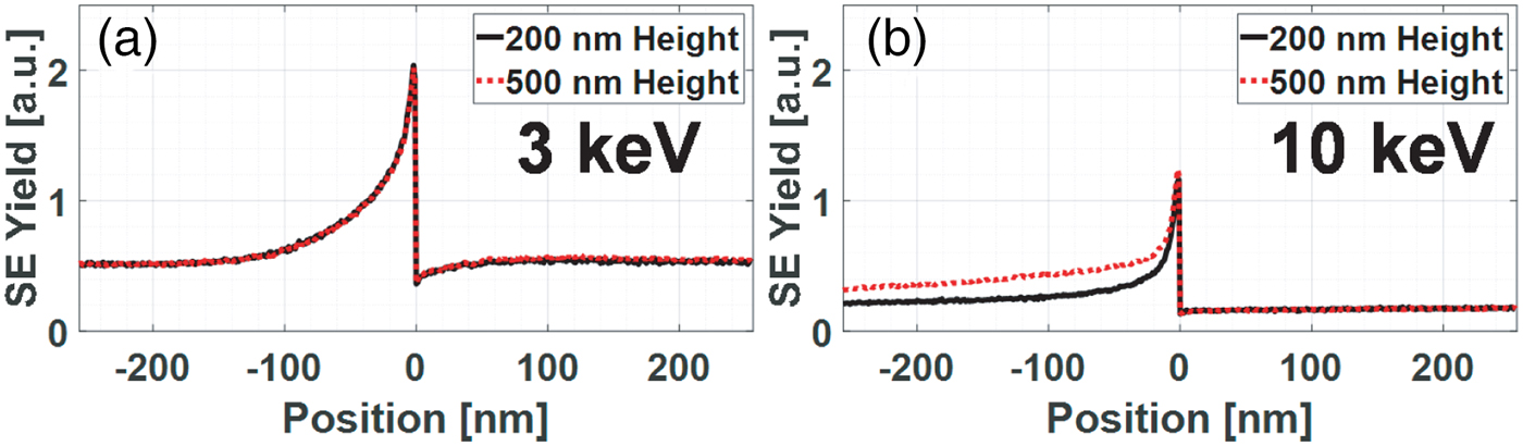
Fig. 3. SE-signal when scanning a PE beam of 3 and 10 keV over two step edges of 200 and 500 nm. a: The depth of the interaction is within the range of the step height at 3 keV and (b) more electrons intersect with the sidewall of the 500 nm step edge, leading to a larger signal intensity at 10 keV.
At 10 keV, electrons penetrate more than 200 nm in the material, where they intersect with a larger surface area on the sidewall of the 500 nm step (Figs. 1, 2c, 2d) than the 200 nm step. Therefore, the SE-signal for the two step heights will be different (Fig. 3b) and that difference allows for the determination of the height difference. It is seen that the signal difference extends quite a distance away from the edge. Close to the edge, the signal may be influenced by the actual topography of the step edge, i.e., sidewall angle or edge rounding. To judge which portion of the signal is rather insensitive to such influences, and can therefore be used for the height determination, a few realistic step topographies are simulated first.
First, the effect of sidewall angle on line scans is investigated, with −5° and +5° deviations of a 90° sidewall. Figure 4a shows the 90° sidewall. Figure 4b has a negative sidewall angle and the dip at the foot of the steep signal drop disappears. Figure 4c has a positive sidewall angle, and an additional feature appears in the peak of the signal. The comparison shows that the signal intensities in the peak and at the foot are very sensitive to variation in the sidewall angle. Therefore, the signal around the peak is to be avoided in the height analysis.
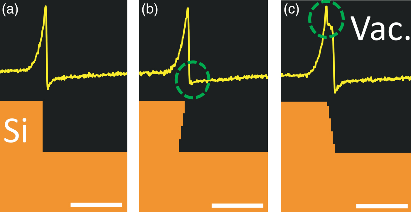
Fig. 4. Effect of sidewall angle of a Si step edge on the SE line scan signal: (a) 90° sidewall, the signal has a peak and a dip at the foot; (b) −5° sidewall angle, creating an undercut, the dip at the foot disappears; and (c) +5° sidewall angle, an additional feature shows up in the peak. The scale bar is 100 nm and the beam energy is 1 keV.
It is also expected that the beam spot size will influence the scan signal near the step edge. Figure 5 shows the simulated line scan over the 500 nm step height for four different spot sizes. The peak and the dip at the foot of the signal are both very sensitive to the beam spot size. However, the lateral region between −64 and −4 nm shows the same intensity for spot sizes smaller than 3 nm (full width at half maximum; FWHM), i.e., step height analysis in this region is insensitive to spot size variations. The 10 nm spot, however, provides so much blur that height information and spot-size effects will be difficult to separate.
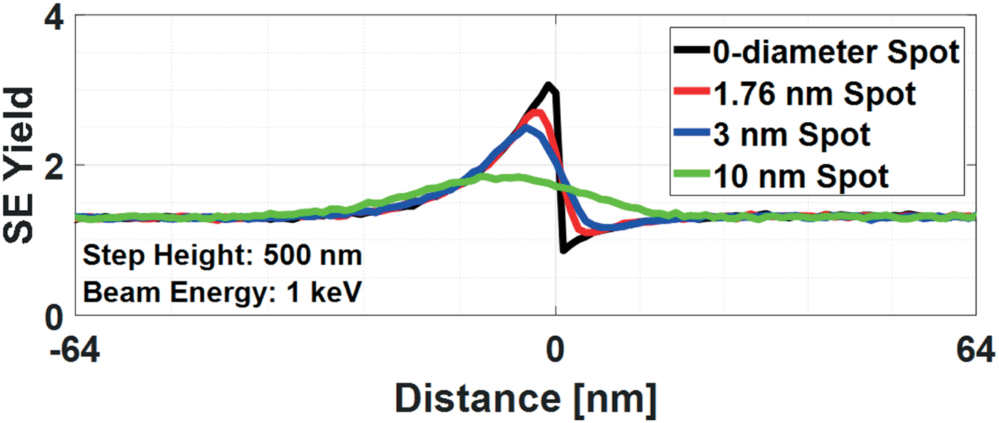
Fig. 5. Spot size effect: the intensity and the position of the peak and the dip of the signal change with the incident beam diameter (FWHM).
Finally, the effect of slightly more realistic edge shapes on the line scan signals was simulated. Two infinitely long lines of different heights are placed at a pitch of 2 µm. Figure 6 shows the cross-sectional view of these lines. The left edges of the lines have perfectly sharp edges with a 90° sidewall. The right-hand side edges have different curvatures.
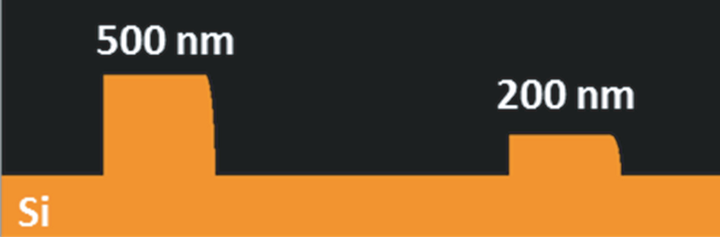
Fig. 6. Cross-section of lines of 500 and 200 nm in height. The top and the bottom widths of the lines are 500 nm, resp. 550 nm. The pitch is 2 µm. The left sidewalls of the structures are sharp vertical edges. The right edges are rounded and the sidewalls follow the curvature of the edge.
Line scans were simulated at two different energies, 3 and 10 keV, and shown in Figure 7. The signals were aligned in order to clearly see the differences. In Figure 7a, the signals are identical for the left edge, but not for the right edge. At 3 keV, the effect of the edge shape and the sidewall angle is seen, but not the effect of the height difference. In Figure 7b, when the energy is increased to 10 keV, the signal for the 500 nm step at the left side edge becomes different. This difference is even more visible all the way into the valley between both edges. Although the peak (intensity and shape) of the signal is very sensitive to the height, as well as all other imperfections close to the edge, fortunately the region in between the edges is less sensitive to the position of the edge and the shape of the sidewall, and still sensitive to the step height difference.

Fig. 7. Line scan signal sensitivity to height differences and sidewall shape differences. The line scans are simulated for the structures in Figure 6 at (a) 3 keV and (b) 10 keV, and a zero-diameter beam. In total, 104 electrons were used per pixel.
The analysis from simulations above demonstrates that there is a region in the line scan signal that is sensitive to height but not sensitive to the electron beam size and the actual edge shape. To make the height determination analysis more quantitative and less sensitive to the noise level, the area below the scan signal in the height sensitive region will be determined. Even if the noise level is high in SEM, integration over the signal (area) is a powerful noise suppression technique and will allow us to differentiate the step heights. This requires, first of all, the determination of the edge position as a reference point. This problem has also been addressed in the literature concerning CD measurements (Karabekov et al., Reference Karabekov, Zoran, Rosenberg and Eytan2003; Tanaka et al., Reference Tanaka, Villarrubia and Vladár2005; Villarrubia et al., Reference Villarrubia, Vladár and Postek2005Reference Villarrubia, Vladár and Posteka, Reference Villarrubia, Vladár and Postek2005b; Shishido et al., Reference Shishido, Tanaka and Osaki2009). Although the model-based-library approach (Shishido et al., Reference Shishido, Tanaka and Osaki2009) is a more accurate method, for practical reasons here the maximum intensity method is preferred, i.e., the edge position is assumed to be at the location where the signal attains a maximum. An example line scan signal, f s, is shown in Figure 8, where the peak indicates the edge position. The vertical dashed lines a 1 and a 2 indicate the left and right boundaries, respectively, between which the area below the signal is to be determined by integration. The right boundary a 2 needs to be chosen sufficiently far from the edge to avoid edge topography influences, as discussed above. The baseline level, f b, determined by the SE yield at the beam energy used and by the brightness settings of the microscope, is subtracted from the signal.
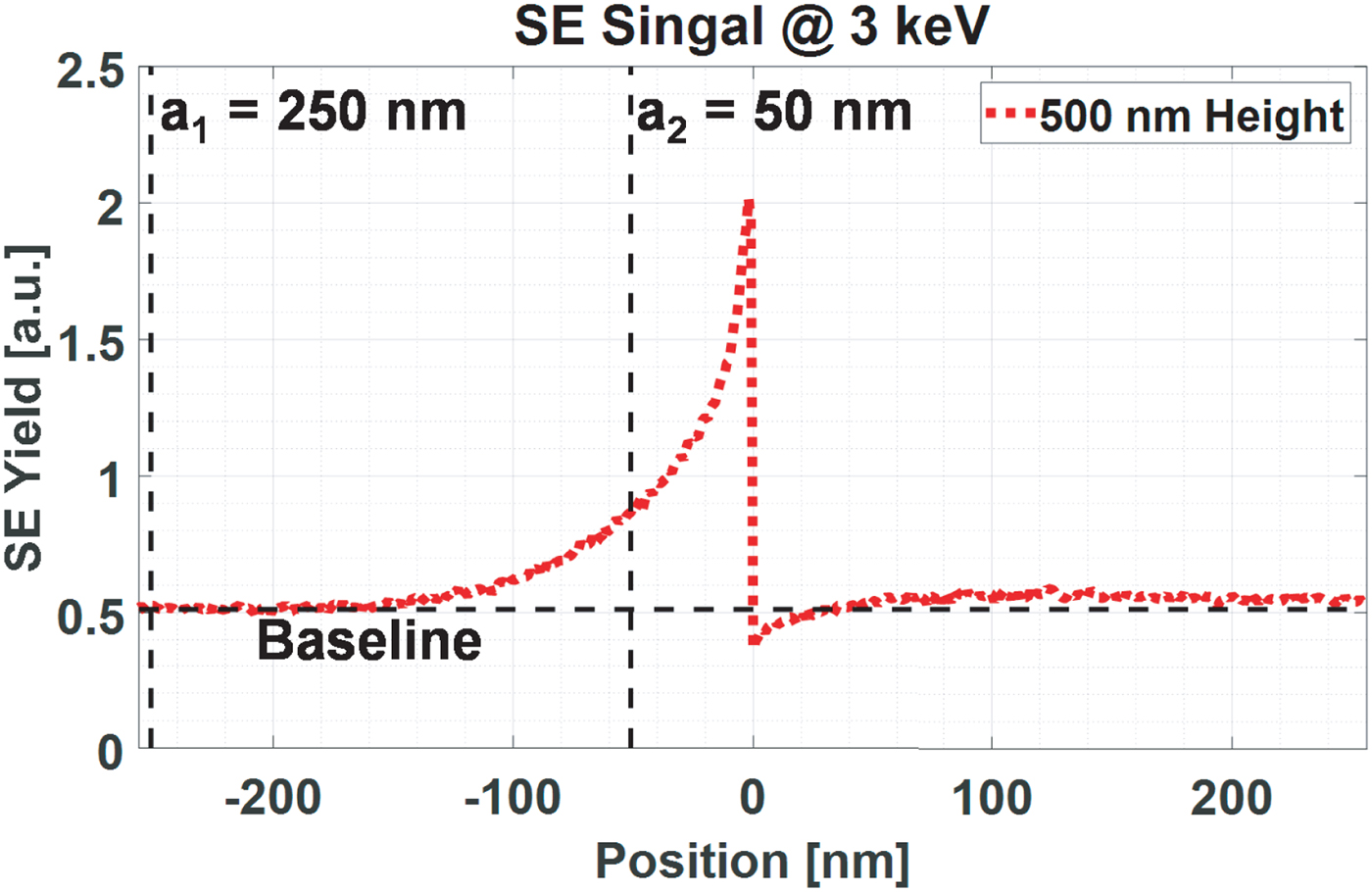
Fig. 8. Illustration of the signal integration method. A simulated line scan signal of a 500 nm high step is shown as the red dotted line; the edge position is taken where the intensity is maximum; the integration boundaries are drawn by the two vertical dashed lines at a 1 (250 nm) and a 2 (50 nm) from the edge.
In brief, the height sensitive information, I h is given by
 $$I_{\rm h} = \int_{a_2}^{a_1} {[\,f_{\rm s}(x)-f_{\rm b}]dx} $$
Figure 9 shows the integrated area, I h for simulated scan signals over different step heights integrated between 250 and 50 nm away from the edge and for beam energies ranging from 100 eV to 20 keV.
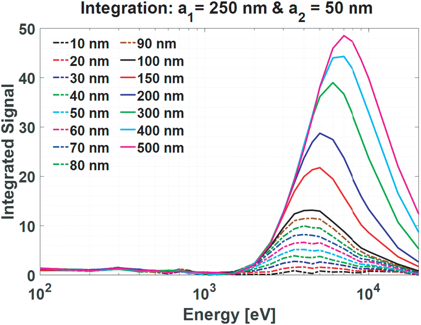
Fig. 9. Integrated area below the line scan signals over step edges of various step heights and as a function of incident electron energy.
Initially the integrated signal increases with energy, as the interaction volume increases as well as its intersection with the sidewall of the step edge. When the interaction volume reaches depths larger than the step height, the integrated signal reaches a maximum, and decreases for even higher energies where less and less electrons can escape from the sample. The overlapping curves at low energies prevent resolving step heights at low energies. But at higher energies the curves are well separated.
For instance, at 1 keV one cannot distinguish the height difference between a 200 and a 500 nm step, but at 8 keV one easily can. To determine the best energy to distinguish step heights Figures 10a and 10b show the integrated signals of Figure 9 plotted versus step height for various primary energies. It is clearly seen that energies lower than 2 keV are not useful to distinguish step heights between 10 and 500 nm.
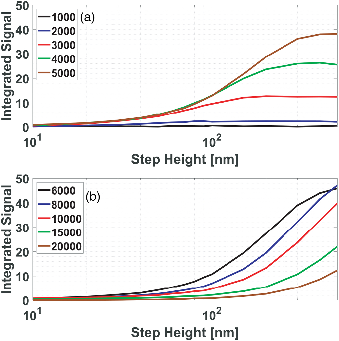
Fig. 10. Integrated signal versus step height for primary energies between 1,000 eV and 20 keV.
Only at higher energies do the curves start to increase with step height. At 5 keV heights up to 300 nm can be distinguished, although the height difference between 10 and 20 nm steps is better detected at lower energy, e.g., 3 keV. Figure 10b shows that at 6 keV larger step height differences up to 500 nm can be detected, but at even higher energies the sensitivity decreases.
From Figure 9 it is clear that to distinguish steps from each other in a set of step heights, the best energy to use is the energy where the integrated signal of the largest step height in the set attains its maximum. Figure 11 shows the step height versus the energy, where the integrated signal is at maximum for that particular step height. It needs to be pointed out that the simulation results shown so far are affected by the particular choice of the integration boundaries. Figure 11 also shows results for other choices of the integration boundaries. If the integration window is narrowed from the left (a 1) the maxima of the step height curves in Figure 9 are pushed to lower energies for higher steps. If the integration window is narrowed from the right (a 2) the smaller step height curves are pushed to higher energies. But in both cases, it remains possible to find a best energy to distinguish between step heights.
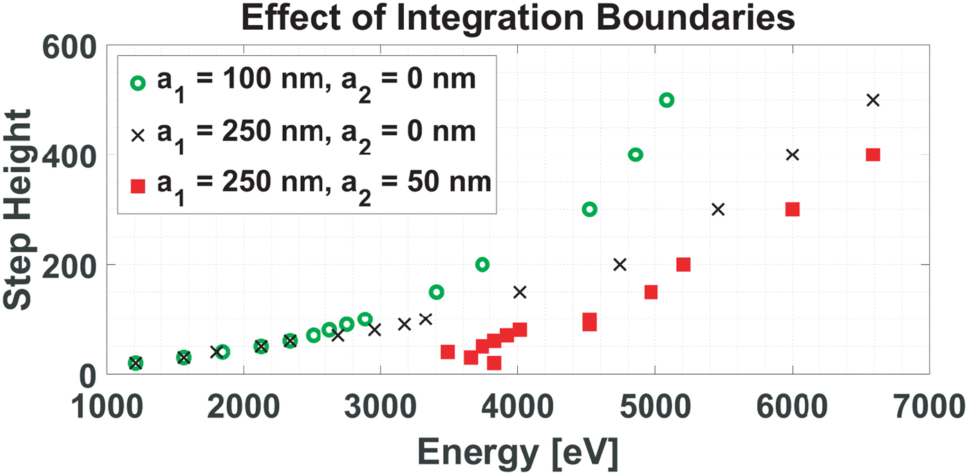
Fig. 11. The effect of the integration boundaries on the step height versus energy where the integrated signal is at maximum. Crosses (×) are for boundaries 250 nm to edge (50 nm); squares (■) indicate that the area is narrowed from the right (boundary a 2) and circles (●) indicate that the area is narrowed from the left (boundary a 1).
Experiments
To validate the technique, we have performed experiments on two available samples: (i) a grating coupler of a photonic integrated circuit (smaller step heights) and (ii) an inverted pyramid (larger step heights).
In Figure 12, a cross-sectional view along the center of the device is sketched. The device consists, from bottom to top, of a 2 µm thick silicon dioxide (SiO2) slab and a 55 nm thick Si slab. These are supported by a Si substrate (not shown). There are three different structures: (i) the waveguide (on top of the Si slab), thickness ~165 nm; (ii) the grating couplers (trenches in the top surface), trench depth ~70 nm; and (iii) the trenches in the 55 nm thick Si slab, all the way down to the SiO2 (the bright rectangles in Fig. 13), trench depth ~55 nm. The latter one is not included in this study due to possible charging effects around the oxide.
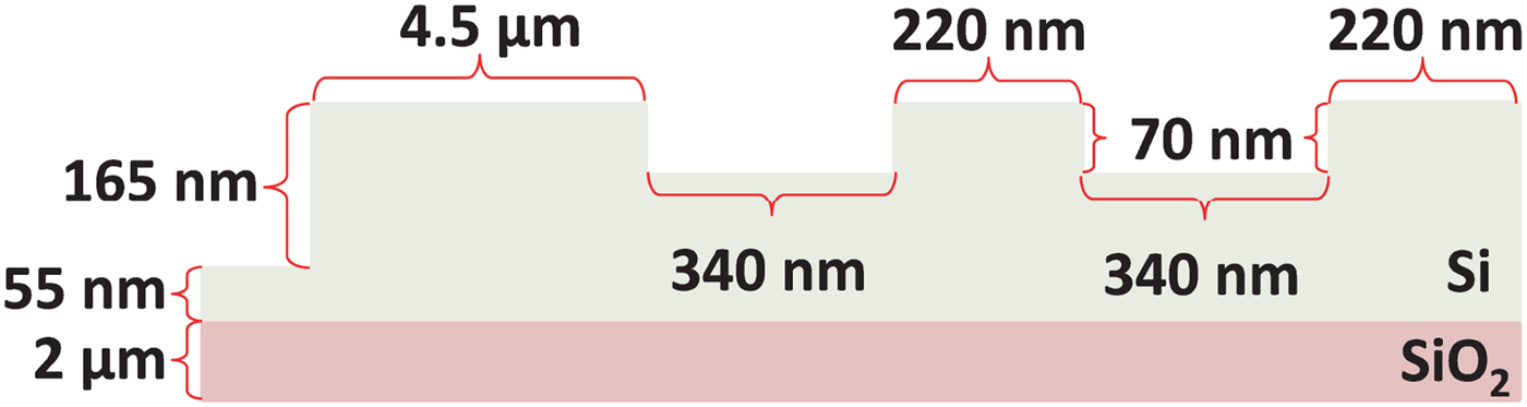
Fig. 12. Description of the grating coupler geometry: the step height determination was performed for the 165 and 70 nm steps only.
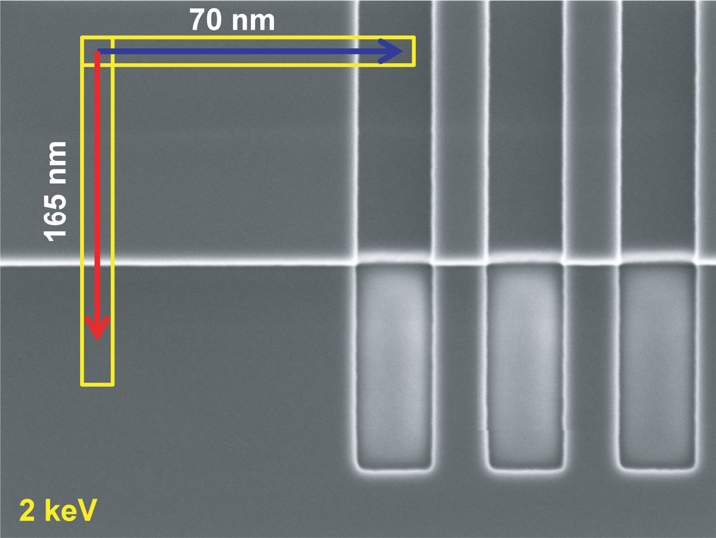
Fig. 13. Top-down SEM image of the grating coupler at 2 keV. HFW: 2.969 µm. Regions are indicated where the line scans are made. Line scans are averaged over the yellow frames along the corresponding arrows. The arrows point from a higher to a lower position.
Several SEM images of the grating coupler were acquired, at the AMO cleanroom facility, at energies ranging from 0.5 to 20 keV, using a Zeiss Supra 60 VP SEM (Oberkochen, BW, Germany) with an in-lens detector. The beam was manually re-focused for each acceleration voltage. All other parameters were kept constant (pixel size = 2.9 nm, working distance = 3.0 mm, contrast = 35.6%, brightness = 49.9%).
In Figure 14, the line scan signals are aligned by their peak positions and plotted on top of each other for demonstration purposes. As the beam energy is increased, the signals start to differ from each other. This very first comparison qualitatively illustrates that the step heights are different and it shows which step is the larger one of the two.
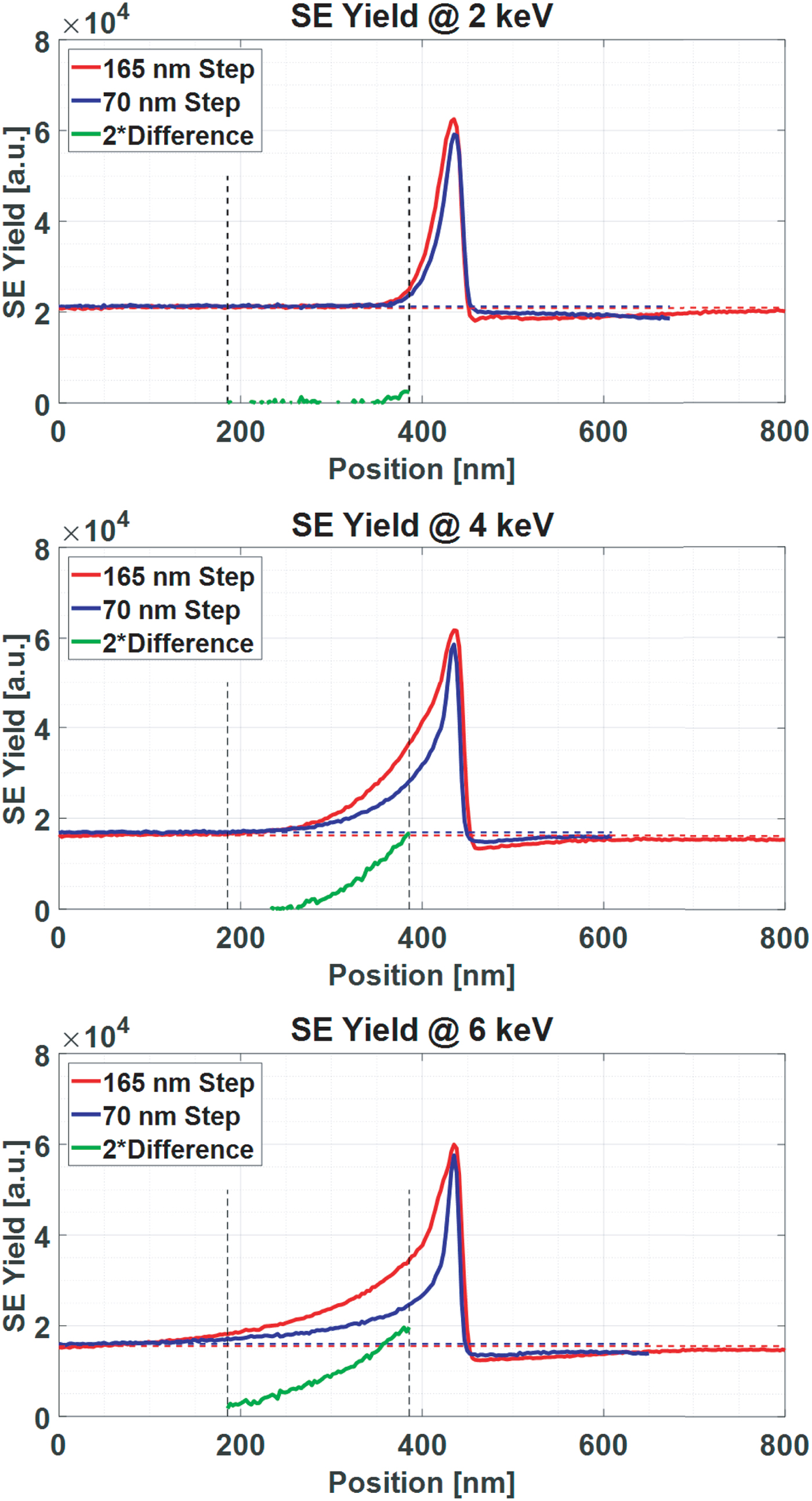
Fig. 14. Experimental step height comparison for the grating coupler sample. Two different step heights are compared at different beam energies. The vertical dashed lines indicate the region where the signal is less sensitive to geometric imperfections. The green curve “2x Difference” indicates the difference signal, i.e., “70 nm Step” subtracted from “165 nm Step” and then multiplied by 2.
Next, the signal integration method is applied with the same integration boundaries as used in the simulations, and the result is shown in Figure 15. The integrated signal for the lower step (70 nm) reaches its maximum at 5.6 keV. Using the simulation results in Figure 11 this maximum energy corresponds to a step height of ~251 nm. Similarly, the integrated signal for the higher step (165 nm) reaches its maximum at 6.48 keV, which corresponds to a simulated step height of ~393 nm. Both values are overestimated. However, 50 nm as the upper integration boundary a 2 is a large value for a small step height (70 nm). If a 2 is lowered to 10 nm, the method estimates the 70 nm step height as 189 nm. As expected, this change does not influence the larger step (398 nm). The ratio of the estimated heights becomes 2.10 (398 nm /189 nm), compared with the actual ratio of 2.35 (165 nm /70 nm).
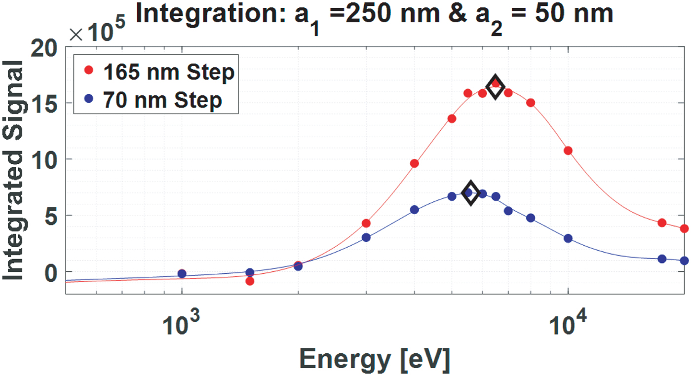
Fig. 15. Integrated signal analysis for the grating couplers. The signals reach a maximum at 5,600 eV (70 nm) and 6,480 eV (165 nm), which are marked by diamonds (◊).
The second sample is a staircase-like sample with a cross-section that looks like an inverted pyramid (see Fig. 16). The structures were fabricated using optical lithography and dry etching. A regular pattern of lines and spaces was first defined on the sample and then etched ~500 nm deep into the silicon. Next, the sample was cleaned and, using the same mask, shifted by 700 nm, and with an identical etching process a second etch depth was realized. The same cycle was repeated three more times to create an inverted step pyramid with five steps, each step ~500 nm deep and 700 nm wide.
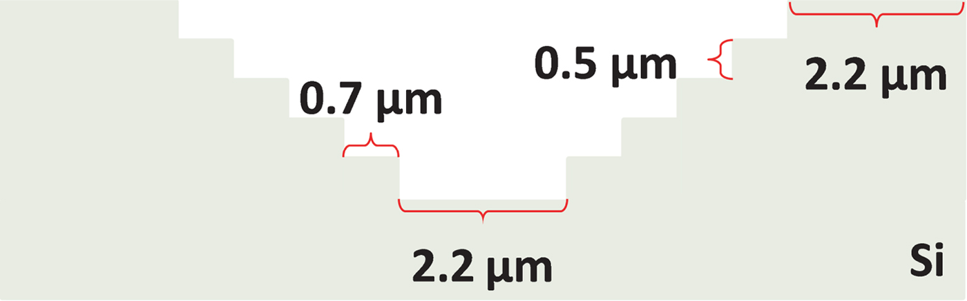
Fig. 16. Cross-section of the inverted pyramid Si sample: from top to bottom five steps are present at each side. Nominally, each step height is 500 nm and the step width is 700 nm. Top and bottom widths are 2.2 µm.
Atomic force microscopy (AFM) measurements were performed to measure the step heights at two different locations on the same set of lines. The line scans shown in Figure 17 show the same step height but the step heights deviate from the nominal value (500 nm) and are also different from each other. The maximum difference is 135 nm and the minimum difference is 26 nm.
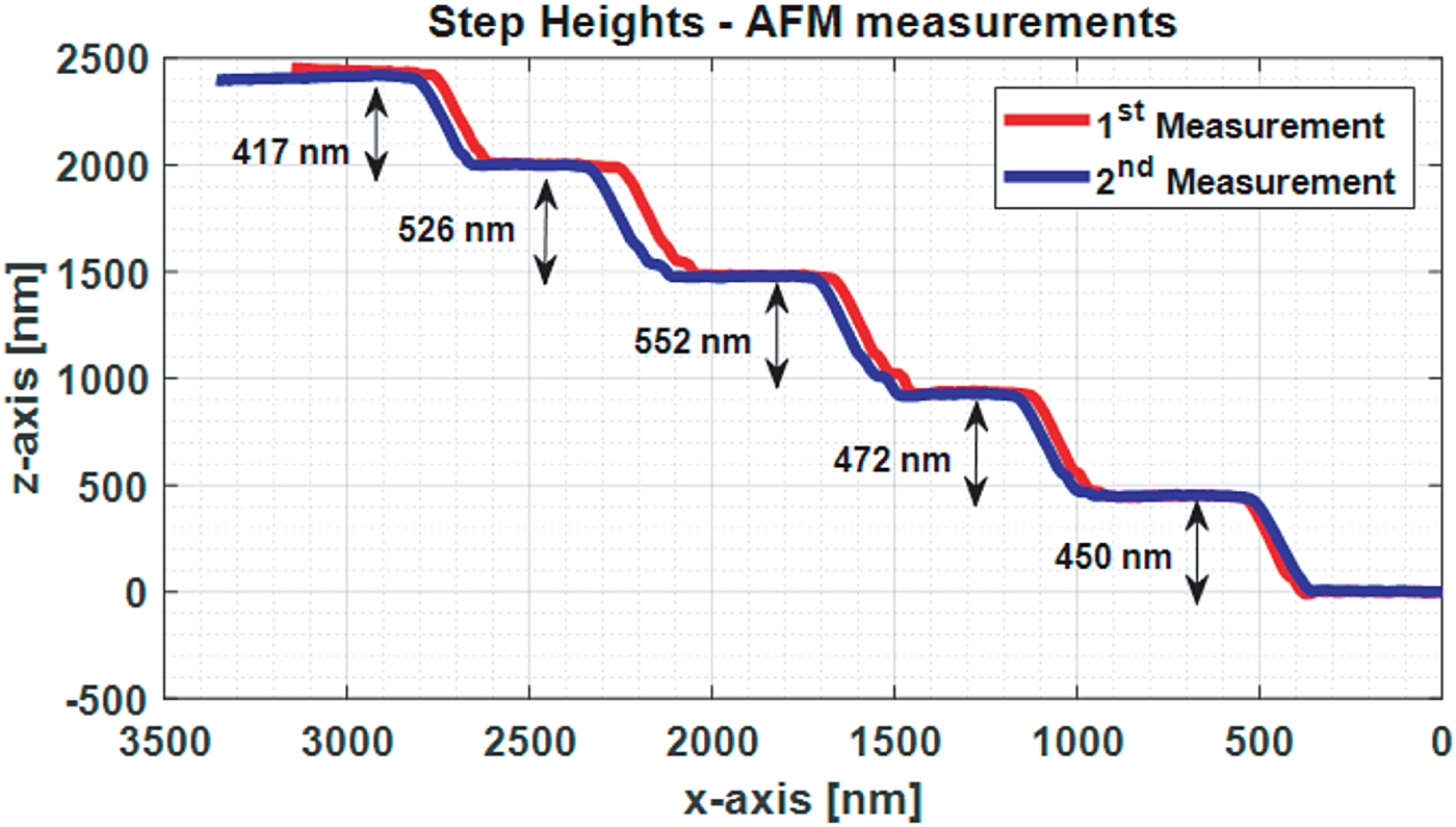
Fig. 17. AFM measurements of the step heights in the inverted pyramid sample.
A top-down SEM image is shown in Figure 18. The SEM images were acquired at the AMO cleanroom facility with the same instrument in which the grating coupler was imaged. Images were taken at 42 different energies between 0.5 and 20 keV. For each acceleration voltage the beam was manually refocused. Moreover, inspection was performed at a new region along the same line in order to minimize potential contamination from the previous acquisition. The entire acquisition process took approximately 30 min. All other parameters were kept constant [horizontal field width (HFW) = 10.035 µm, pixel size = 9.8 nm, working distance = 2.8 mm, contrast = 32.4%, brightness = 50.6%].
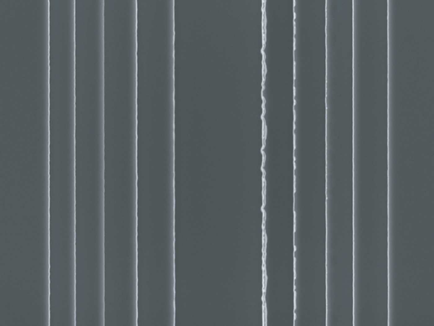
Fig. 18. Top-down SEM micrograph of the inverted pyramid at 4 keV.
In the analysis the right-hand side stairs in Figure 18 are not included because of the irregularities seen in the fourth and fifth edges from the right. Also, it should be noted that the left most (the first) step is geometrically not quite identical to the others. All other steps have an obstacle (another step) to their left-hand side, which may prevent emitted electrons from reaching the detector. Therefore, the first step cannot be compared well with the other steps and is excluded from the analysis. The line scan plots can be found in the supplementary document. The integrated signals are plotted versus energy for all steps in Figure 19.
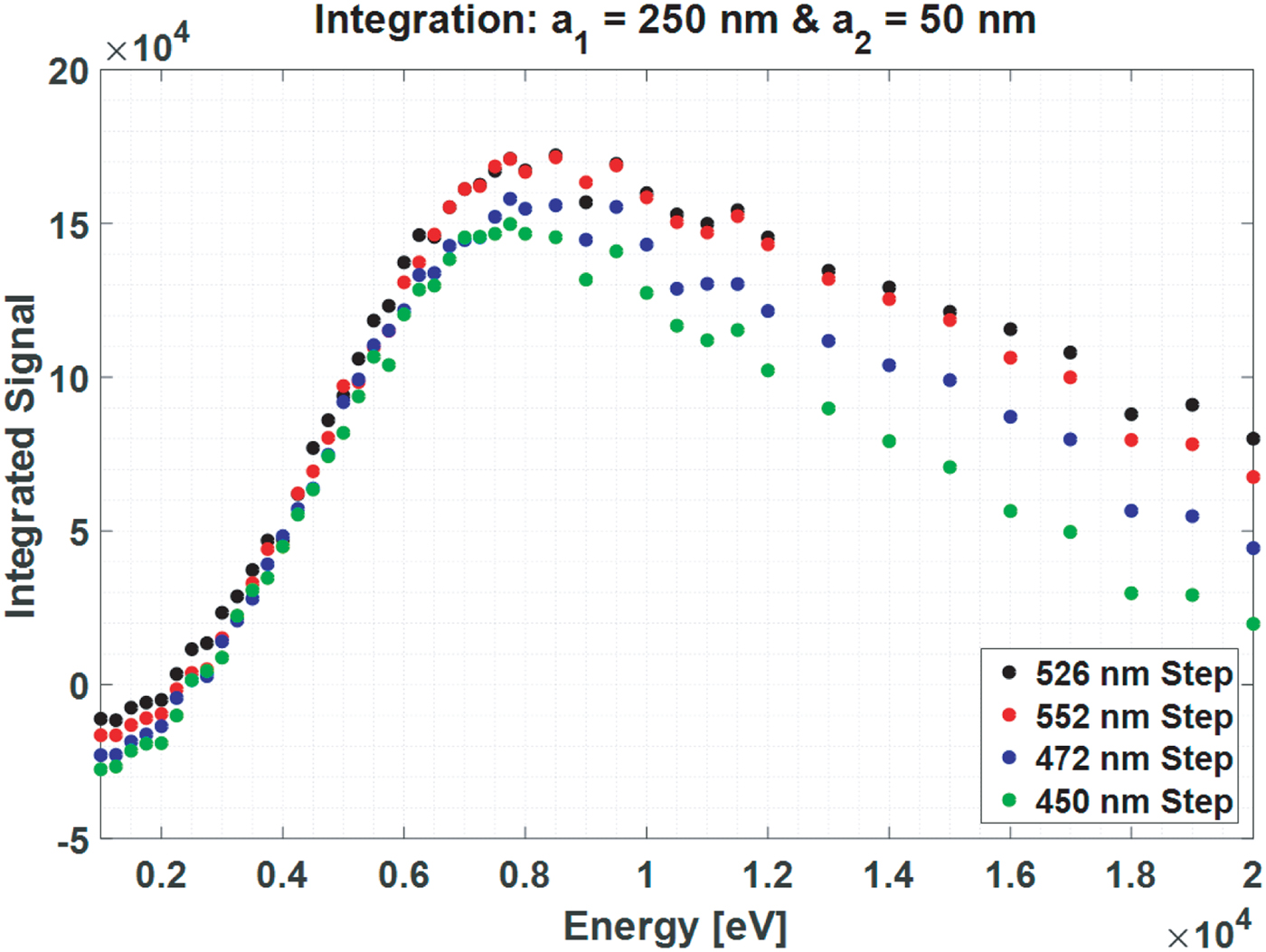
Fig. 19. Integrated signal analysis of the inverted pyramid for the images acquired with a Zeiss Supra SEM (a 1 = 250 nm and a 2 = 50 nm).
There is some general agreement between the experiments and the simulations: the integrated signals coincide at low energies and at higher energies the higher step gives a larger signal. Only at very high energies (~20 keV) deviation is observed: the 526 nm step gives a larger signal than the 552 nm step.
To learn how the result of this analysis depends on the specific imaging tool used and the experimental conditions, a sister sample from the same wafer was imaged using a Raith eLINE Plus system (Dortmund, NRW, Germany). At Raith's cleanroom facility the same procedure was followed as used at AMO and subsequently plasma cleaning was applied for 15 min before inspection to minimize carbon deposition. For all energies the following parameters were kept constant: Field of view (FoV) = 6.0 µm, pixel size = 2.0 nm, working distance = 6.6 mm, contrast = 25.1%, and brightness = 49.3%. Figure 20 shows an SEM image of the left stairs of the sample at 4 keV.
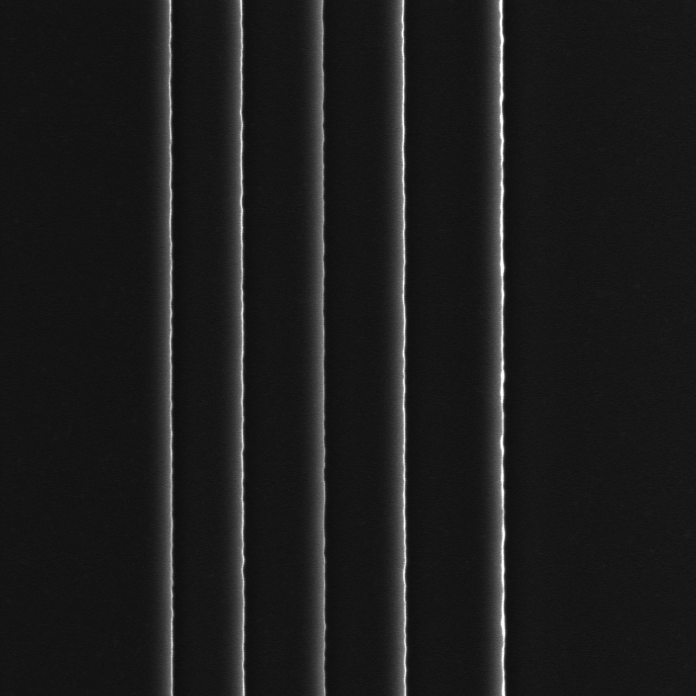
Fig. 20. Top-down SEM image of the steps (only left-side) at 4 keV. FoV = 8.0 µm, taken with the RAITH eLINE Plus SEM.
The integrated signals of the line scans over these steps are shown in Figure 21. At higher energies (20 keV), the results are in conflict with the AMO results of Figure 19, but agree with the simulation results. However, at lower energy (<10 keV), deviations from the simulations are observed: the signal of the 450 nm step is larger than the signal of the 526 nm step.
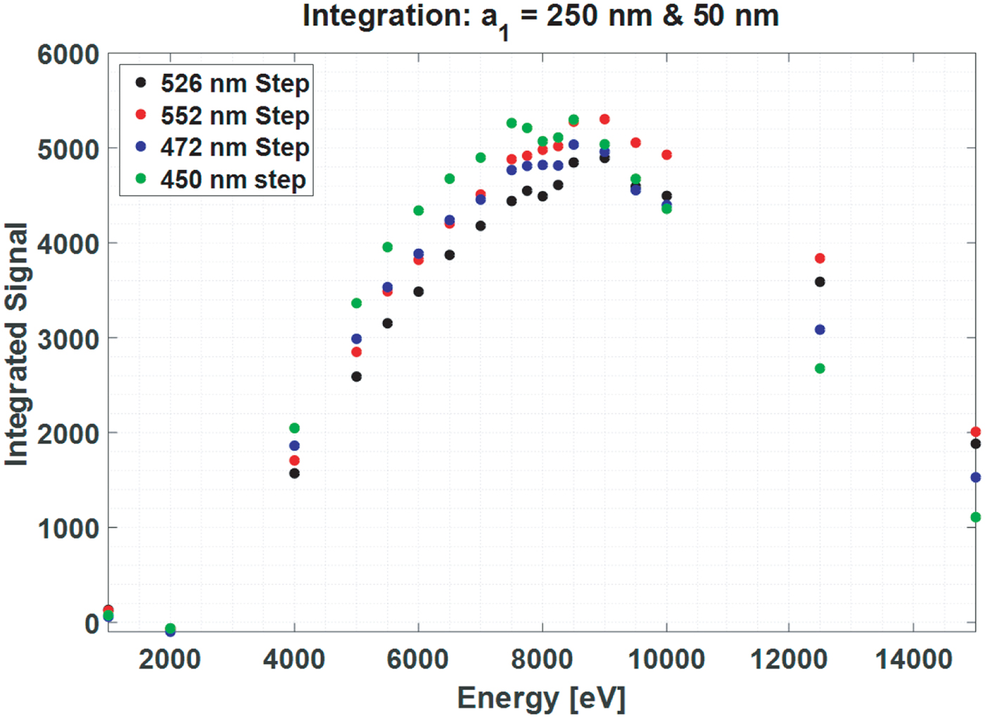
Fig. 21. Integrated signal analysis of the inverted pyramid using images acquired with the Raith eLine plus SEM (a 1 = 250 nm and a 2 = 50 nm).
Similarly, as was done with the simulation results, in Figure 21 the height of each step, analyzed in the AMO and Raith experiments, is plotted versus the energy where the integrated signal of the line scan over that step is maximum. The simulation data are also replotted.
The experimental results show a similar trend to the simulation results, i.e., for larger step heights the peak of the integrated signal versus energy curve shifts to higher energy. The simulated integrated signals peak at energies about 1.5 keV lower than the experimental signals, which all seem to lie close to a universal curve.
Discussion
The results show that by using the proposed method, height differences in step-like structures can be easily distinguished from top-down SEM images. This gives metrologists a quick impression of height differences in structures in a very early stage of the inspection. But the quantification of the actual step heights still leaves something to be desired. The simulation results being shifted to lower energies than the experimental data in Figure 22 is something that needs an explanation. Possible causes could be:
(1) The scattering models in the simulator do not sufficiently well describe the reality yet.
(2) The sample that is being simulated is likely to be an idealized version of the real sample, which is probably covered with surface oxides, contamination layers, layers of water, etc. Specifically in the case of the grating coupler, at higher energies (3 keV) electrons will penetrate into the underlying silica layer, thereby influencing the size of the interaction volume, where in the simulation the sample consisted of Si only. And the results of the staircase-shaped-inverted pyramid sample may very well be influenced by extra emission or absorption, that is not present in the simulated isolated step edge.
(3) Operation and tool effects (Postek & Vladár, Reference Postek and Vladár2013) such as the detection efficiency, which is not taken into account yet in the simulation. It is interesting to see that, although the trends in the experimental results qualitatively agree with each other, the two different AMO experiments are located at lower energies (Fig. 22), but the Raith experiments are shifted toward higher energies. Furthermore, having automated acquisition systems such as an automated focusing function would decrease possible operator influence on the results. However, brightness and contrast values should be fixed.
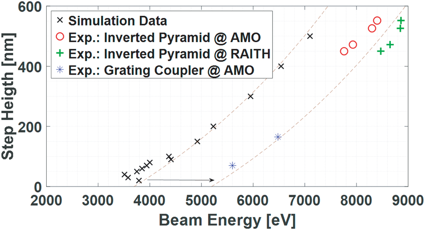
Fig. 22. Simulations and experiments compared: step height versus energy where the integrated signal attains its maximum (a 1 = 250 nm and a 2 = 50 nm). The shift shown between the dashed lines is 1.5 keV.
The method was demonstrated using step edges, but is not limited to step edges only. It can also be applied to narrow lines. This could even give a better contrast because the emission difference will originate from two sidewalls instead of one. However, one needs to consider the region omitted from the signal in the analysis. In this study 50 nm near the peak in the scan signal was omitted, which can clearly not be done for lines narrower than 50 nm. In that case a smaller region needs to be omitted, meaning that a better knowledge of the edge geometry is required.
Unfortunately, the method presented cannot be used in CD-SEMs as it is, which are mostly operated at low voltages 300–800 eV (Orji et al., Reference Orji, Badaroglu, Barnes, Beitia, Bunday, Celano, Kline, Neisser, Obeng and Vladar2018). Figures 9 and 10 show that 300 eV cannot resolve height information above 10 nm.
The method explained here, to find the energy that gives the maximum integrated signal, can be laborious in case there is no auto-focus function of the tool. In that case, it would suffice to take images at three different energies and apply a Gaussian-type fit to find the maximum.
Conclusions
In this study step heights were determined from top-down SEM images, using Monte Carlo simulations and experiments. It was shown that the SE signal, when scanning over an edge, is very sensitive to various factors such as the actual edge shape, sidewall angle, beam spot size, but also the height of the structure. Using Monte-Carlo simulations it was discovered that part of the scan line signal is sensitive to height but not sensitive to the other parameters stated above. This enables the use of standard top-down SEM images for the height measurement of step-like features. A practical method has been introduced to quantify the heights from top-down images. The method has been applied on three different samples that were imaged in two different SEMs. The step heights of samples were measured using AFM. The method consists of acquiring a series of top-down SEM images at a range of PE energies. The integrated scan line signals, when scanning over a step edge, show a maximum for a specific energy (E max). The step heights, as determined from the AFM measurements, are found to lie close to a universal curve when plotted versus the experimentally determined E max. Furthermore, this curve is in qualitative agreement with the simulation results. More data, on various samples, and in various tools, may provide more confidence in the method proposed, and will aid in making the method more quantitative.
Finally, this work is a nice example of how Monte-Carlo simulations can be used to analyze a complex scenario. Without the insight obtained by the simulations it would be very difficult to deduce such knowledge from experiments.
Supplementary material
The supplementary material for this article can be found at https://doi.org/10.1017/S143192761900062X.
Author ORCIDs
Kerim Tugrul Arat, 0000-0002-5446-3006.
Acknowledgments
We are grateful to Gaudhaman Jeevanandam and Luc van Kessel for reading and correcting the manuscript. We are thankful to Martin Kamerbeek for AFM measurements. We also acknowledge GenISys-GmbH and Raith B.V. for funding the research project on modeling of electron–matter interactions.


 Open access