Hostname: page-component-76fb5796d-dfsvx Total loading time: 0 Render date: 2024-04-26T13:54:03.421Z Has data issue: false hasContentIssue false

Electrical and optical characteristics of solution-processed MoOx and ZnO QDs heterojunction

Published online by Cambridge University Press:  10 August 2017

Hemant Kumar*
Affiliation:
Department of Electronics Engineering, Indian Institute of Technology (Banaras Hindu University), Varanasi 221005, India
Yogesh Kumar
Affiliation:
Department of Electronics Engineering, Indian Institute of Technology (Banaras Hindu University), Varanasi 221005, India
Gopal Rawat
Affiliation:
Department of Electronics Engineering, Indian Institute of Technology (Banaras Hindu University), Varanasi 221005, India
Chandan Kumar
Affiliation:
Department of Electronics Engineering, Indian Institute of Technology (Banaras Hindu University), Varanasi 221005, India
Bratindranath Mukherjee
Affiliation:
Department of Metallurgical Engineering, Indian Institute of Technology (Banaras Hindu University), Varanasi 221005, India
Bhola N. Pal
Affiliation:
School of Material Science and Technology, Indian Institute of Technology (Banaras Hindu University), Varanasi 221005, India
Satyabrata Jit*
Affiliation:
Department of Electronics Engineering, Indian Institute of Technology (Banaras Hindu University), Varanasi 221005, India
*
Address all correspondence to Hemant Kumar, Satyabrata Jit at hkumar.rs.ece13@iitbhu.ac.in, sjit.ece@iitbhu.ac.in
Get access

Abstract

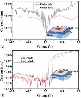
In this work, effects of heat treatment on the heterojunction between MoOx and ZnO quantum dots (QDs) are analyzed possibly for the first time. Solution-processed and thermal deposition technique is used for the growth of MoOx over the ZnO QDs and compared for the electrical analysis. The absorption and photoluminescence properties of ZnO QDs and MoOx have been analyzed for the optical behavior. Further, the heat-treated heterojunctions are analyzed for built-in potential (0.25 V), carrier density (~2.9 × 1018 cm−3), and responsivity (3.93 mAW−1). The heterojunction of solution-processed MoOx and ZnO QDs shows better stability after heat treatment compared with other devices.

Type
Research Letters
Copyright
Copyright © Materials Research Society 2017 

Access options

Get access to the full version of this content by using one of the access options below. (Log in options will check for institutional or personal access. Content may require purchase if you do not have access.)

References

1.Litzov, I. and Brabec, C.J.: Development of efficient and stable inverted bulk heterojunction (BHJ) solar cells using different metal oxide interfaces. Materials (Basel) 6, 5796 (2013).Google Scholar
2.Lattante, S.: Electron and hole transport layers: their use in inverted bulk heterojunction polymer solar cells. Electronics 3, 132 (2014).Google Scholar
3.Baeg, K.-J., Binda, M., Natali, D., Caironi, M., and Noh, Y.-Y.: Organic light detectors: photodiodes and phototransistors. Adv. Mater. 25, 4267 (2013).Google Scholar
4.Pal, B.N., Robel, I., Mohite, A., Laocharoensuk, R., Werder, D.J., and Klimov, V.I.: High-sensitivity p-n junction photodiodes based on PbS nanocrystal quantum dots. Adv. Funct. Mater. 22, 1741 (2012).Google Scholar
5.Liao, H.H., Chen, L.M., Xu, Z., Li, G., and Yang, Y.: Highly efficient inverted polymer solar cell by low temperature annealing of Cs2CO3 interlayer. Appl. Phys. Lett. 92, 2006 (2008).Google Scholar
6.Wiranwetchayan, O., Liang, Z., Zhang, Q., Cao, G., and Singjai, P.: The role of oxide thin layer in inverted structure polymer solar cells. Mater. Sci. Appl. 2, 1697 (2011).Google Scholar
7.Ionescu-Zanetti, C., Mechler, A., Carter, S.A., and Lal, R.: Semiconductive polymer blends: correlating structure with transport properties at the nanoscale. Adv. Mater. 16, 385 (2004).Google Scholar
8.Kemerink, M., Timpanaro, S., de Kok, M.M., Meulenkamp, E. A., and Touwslager, F.J.: Three-dimensional inhomogeneities in PEDOT: PSS films. J. Phys. Chem. B 108, 18820 (2004).Google Scholar
9.Girotto, C., Voroshazi, E., Cheyns, D., Heremans, P., and Rand, B.P.: Solution-processed MoO3 thin films as a hole-injection layer for organic solar cells. ACS Appl. Mater. Interfaces 3, 3244 (2011).Google Scholar
10.Caruge, J.M., Halpert, J.E., Bulović, V., and Bawendi, M.G.: NiO as an inorganic hole-transporting layer in quantum-dot light-emitting devices. Nano Lett. 6, 2991 (2006).Google Scholar
11.Zilberberg, K., Trost, S., Meyer, J., Kahn, A., Behrendt, A., Lützenkirchen-Hecht, D., Frahm, R., and Riedl, T.: Inverted organic solar cells with sol-gel processed high work-function vanadium oxide hole-extraction layers. Adv. Funct. Mater. 21, 4776 (2011).Google Scholar
12.Tsay, C.-Y., Fan, K.-S., Chen, S.-H., and Tsai, C.-H.: Preparation and characterization of ZnO transparent semiconductor thin films by sol–gel method. J. Alloys Compd. 495, 126 (2010).Google Scholar
13.Liu, K., Sakurai, M., and Aono, M.: ZnO-based ultraviolet photodetectors. Sensors (Basel) 10, 8604 (2010).Google Scholar
14.Wang, Z.L.: ZnO nanowire and nanobelt platform for nanotechnology. Mater. Sci. Eng. R, Rep. 64, 33 (2009).Google Scholar
15.Kumar, Y., Kumar, H., Rawat, G., Kumar, C., Sharma, A., Pal, B.N., and Jit, S.: Colloidal ZnO quantum dots based spectrum selective ultraviolet photodetectors. IEEE Photonics Technol. Lett. 29, 361 (2017).Google Scholar
16.Kumar, Y., Kumar, H., Mukherjee, B., Rawat, G., Kumar, C., Pal, B.N., and Jit, S.: Visible-blind Au/ZnO quantum dots based highly sensitive and spectrum selective. IEEE Trans. Electron Devices 64, 2874 (2017).Google Scholar
17.Rawat, G., Somvanshi, D., Kumar, H., Kumar, Y., Kumar, C., and Jit, S.: Ultraviolet detection properties of p-Si/n-TiO2 heterojunction photodiodes grown by electron-beam evaporation and sol-gel methods: a comparative study. IEEE Trans. Nanotechnol. 15, 193 (2016).Google Scholar
18.Rawat, G., Somvanshi, D., Kumar, Y., Kumar, H., Kumar, C., and Jit, S.: Electrical and ultraviolet-A detection properties of E-beam evaporated n-TiO2 capped p-Si nanowires heterojunction photodiodes. IEEE Trans. Nanotechnol. 16, 49 (2017).Google Scholar
19.Chambon, S., Derue, L., Lahaye, M., Pavageau, B., Hirsch, L., and Wantz, G.: MoO3 thickness, thermal annealing and solvent annealing effects on inverted and direct polymer photovoltaic solar cells. Materials (Basel) 5, 2521 (2012).Google Scholar
20.Yadav, A.B., Pandey, A., and Jit, S.: Effects of annealing temperature on the structural, optical, and electrical properties of ZnO thin films grown on n-Si<100> substrates by the sol-gel spin coating method. Acta Metall. Sin. (English Lett.) 27, 682 (2014).+substrates+by+the+sol-gel+spin+coating+method.+Acta+Metall.+Sin.+(English+Lett.)+27,+682+(2014).>Google Scholar
21.Yadav, A.B., Shankar, R., Kumar, R., Pandey, A., and Jit, S.: Analysis of temperature dependent I–V characteristics of Pd/ZnO/n-Si Schotky diode by sol-gel method. International Conference on Microelectronics, Communication and Renewable Energy (ICMiCR-2013), Koovappally, Kerala, India (2013, pp. 8–11).Google Scholar
22.Yadav, A.B., Singh, K., Pandey, A., and Jit, S.: Annealing-temperature effects on the properties of ZnO thin films and Pd/ZnO Schottky contacts grown on n-Si (100) substrates by vacuum deposition method. Superlattices Microstruct. 71, 250 (2014).Google Scholar
23.Yadav, A.B., Periasamy, C., and Jit, S.: Study of post annealing effects on structural and optical properties of sol-gel derived ZnO thin films grown on n-Si substrate. IOP Conf. Ser. Mater. Sci. Eng. 73, 12060 (2015).Google Scholar
24.Kumar, H., Kumar, Y., Mukherjee, B., Rawat, G., Kumar, C., Pal, B.N., and Jit, S.: Electrical and optical characteristics of self-powered colloidal CdSe quantum dot-based photodiode. IEEE J. Quantum Electron. 53, 1 (2017).Google Scholar
25.Klimov, V.I.: Nanocrystal Quantum Dots, second edn. (CRC Press, Boca Raton, 2010).Google Scholar
Supplementary material: File

Kumar supplementary material

Figures S1-S6

Download Kumar supplementary material(File)
File 9.1 MB