


1. Introduction
Since the first laser with a solid-state flashlamp-pumped synthetic ruby crystal was demonstrated successfully by Theodore H. Maiman in May 1960[Reference Maiman1], laser technology made great progress in the last half century. The coherency, high monochromaticity, and ability to reach extremely high powers are suitable for specialized applications, such as scientific research, medical treatment, and commercial fabrication. The intensity of the lasers has been increased by many orders of magnitude, up to  $1{0}^{22} ~\mathrm{W} / {\mathrm{cm} }^{2} $[Reference Bahk, Rousseau, Planchon, Chvykov, Kalintchenko, Maksimchuk, Mourou and Yanovsky2], and the pulse duration decreased by more than 15 orders of magnitude, down to
  $6. 7\times 1{0}^{- 17} ~\mathrm{s} $, as well[Reference Zhao, Zhang, Chini, Wu, Wang and Chang3]. The National Ignition Facility (NIF)[Reference Miller, Lane and Wuest4] and Laser Mégajoule (LMJ)[Reference Ebrardt and Chaput5], among the world’s most powerful and complex arrangements of multiple lasers, are used to produce extremely high intensity pulses of light with extremely short duration. Optical components, such as high-reflectance mirrors, windows/lenses with antireflection coatings, and polarizers, are widely used for beam steering, surface reflectance reducing, and pulse switching. Due to the involvement of defects during the deposition of thin films and enhanced interference effects, the optical coating is generally the limiting factor in the output energy of a high-power laser system in recent decades. Besides, the surface figure distortion of optical components with coating is another limiting factor for the laser beam focus. The extensive applications of lasers, especially for high-power laser facilities in recent years, have increased the demand for high-performance optical coatings with matched stress for minimum wavefront distortion, high reflectivity or transmission for low energy loss, and high laser resistance for maximum energy output. In this paper, the development of high-power laser coatings by our group is summarized. Section 2 deals with the design of thin films, including the spectral specification, and the temperature field and stress field. Section 3 investigates the deposition process of a laser-resistant coating, including the sub-surface defect control, substrate cleaning, the optimization of deposition parameters and electric field distribution, and post treatment. In Section 4, the stress of optical component is discussed, including the stress match of high and low refractive index materials in multilayer and in situ stress measurement.
2. Design of a high-power laser coating
The design of an optical multilayer coating for a particular application is a rather complicated task, especially for optical coatings in a high-power laser facility. Here, spectral requirements involve the main laser, the alignment laser, and stimulated Brillouin scattering light. With commercial design software, it is now not a challenge to obtain the qualified design to meet the spectral requirements. However, the available laser-resistant materials are limited, and the optical constants of the materials depend on the available coating equipment and deposition process. Furthermore, one must consider the temperature field to show perfect laser resistant capability and the stress field to meet the wavefront requirement. In the 1990s, Fan in our group first proposed a calculation method of the temperature field, and calculated the temperature distribution of a high-reflectance coating due to interface absorption, as shown in Figure 1. Interface absorption plays a great role in the temperature rise in multilayer thin films[Reference Fan and Tang6].

Figure 1. Temperature and electric field distribution in a high-reflectance coating with and without interface absorption.
During the design of a coating, the process tolerance must be considered. Too thin or too thick a layer is not good for the deposition of a thin film. A design with larger tolerance may simplify the production of the coating. Four kinds of polarizer were designed and manufacturing tolerances were evaluated with experiments, as shown in Figure 2. Comparing the theoretical and measured spectrum, it is obvious that the design with larger tolerance can obtain a spectrum closer to the theoretical design[Reference Zhu, Yi, Fan and Shao7].
Figure 2. Designed and measured transmittance spectra of polarizer.
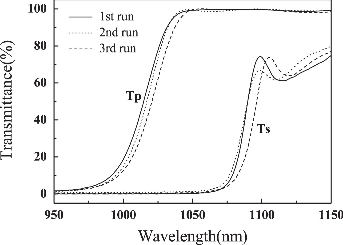
In order to obtain the desired spectral performance, it is essential to precisely control the layer thickness. An automatic thickness monitoring system, combining the optical monitor and the crystal monitor, has been developed in our group. In order to test the control precision of the developed monitoring system, three successive runs for the polarizer were made, as shown in Figure 3. The measured results show nice repeatability of the process[Reference Zhu, Yi, Zhang, Fan, He and Shao8].
Figure 3. Measured transmittance spectra of polarizer for three runs.
3. Deposition of a laser-resistant coating
Under irradiation of high-power laser, the most common failure case of optical coatings results from the absorption defects within the coating or on the coating’s interface with the substrate or air. These absorption defects absorb laser energy, resulting in heat generation that causes localized melting or stress-induced fracture. Therefore, decreasing the defect density and improving the damage performance of the defects are two effective ways to improve the laser-induced damage threshold (LIDT) of the coating. As is well known, the involvement process of defects in multilayer coatings is complicated, and is related to surface and sub-surface defects of the substrate, the cleaning process of the substrate, deposition parameters, post-treatment process, and even the packing process and application environment. Besides, optimization of the electric field distribution can minimize the negative effect of defects on laser-induced damage (LID) of thin films. Therefore, the deposition of laser-resistant optical coatings is systematic engineering. One needs to thoroughly understand the defect source, and take effective measures to tightly control every aspect of the production process.
Sub-surface defect
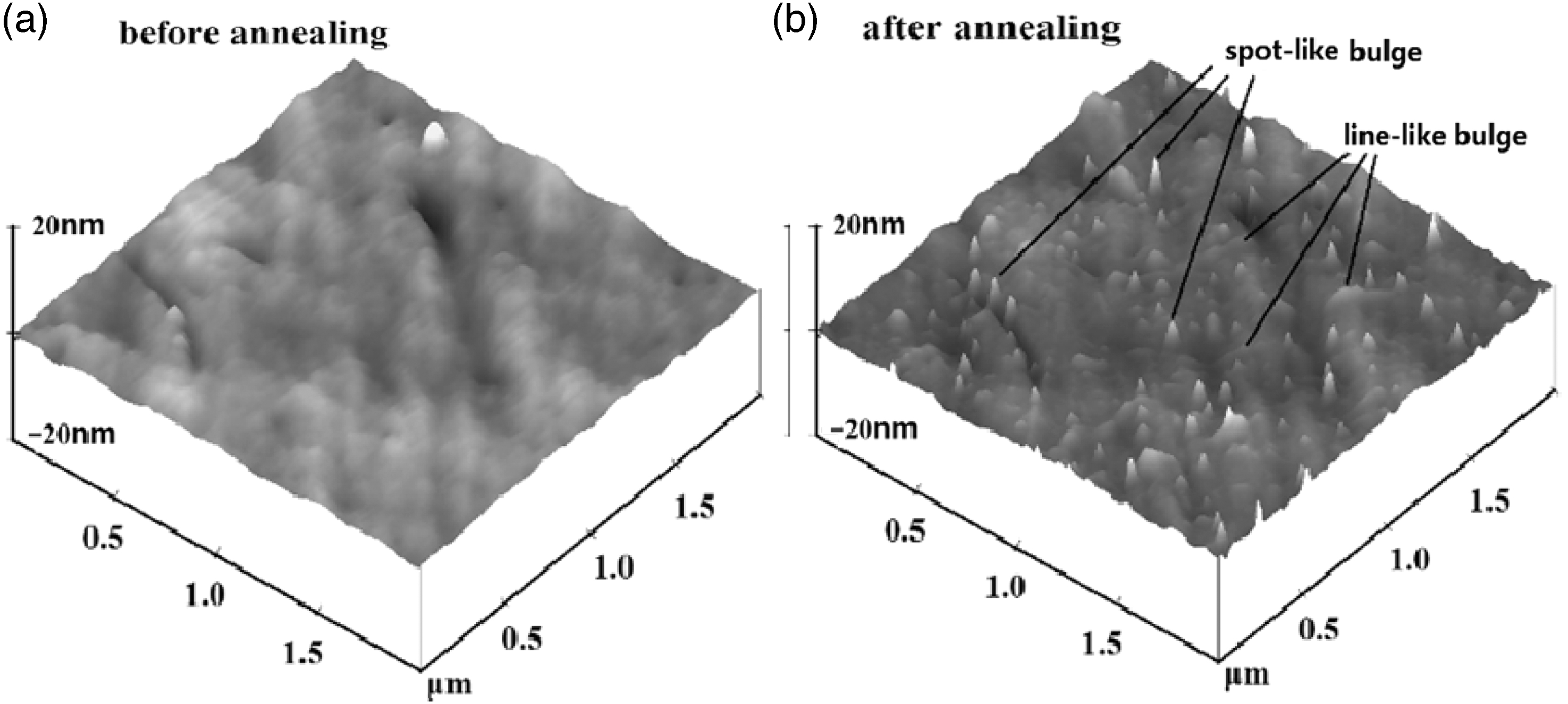
Although the density and size of sub-surface defects decrease rapidly after optimization of the machining, grinding, and polishing process, it is difficult to guarantee that substrates are all free of sub-surface defects. Therefore, the inspection of sub-surface defects of the substrate is an important step before deposition of the coating. In our group, a heat treatment method is used to characterize the sub-surface defects. Examined with an atomic force microscope (AFM), the surface morphology of fused silica substrates can be obtained before and after the annealing process, as shown in Figure 4. It can be seen that a high density of protrusive points, induced by the sub-surface defects, appears on the surface of the substrate after the annealing process[Reference Yang, Zhao, Shan, Yi and Shao9].
Figure 4. Surface morphology of fused silica before and after annealing treatment  $(40{0}^{\circ } / 18~\mathrm{h} )$.
Substrate cleaning process
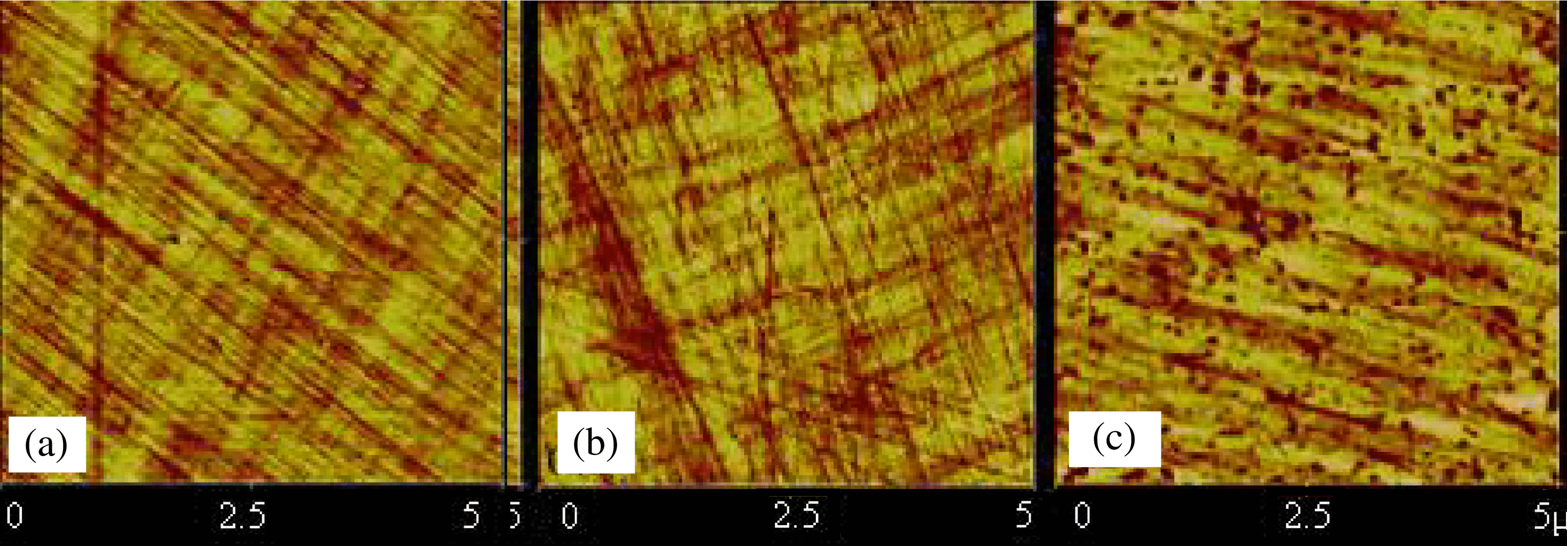
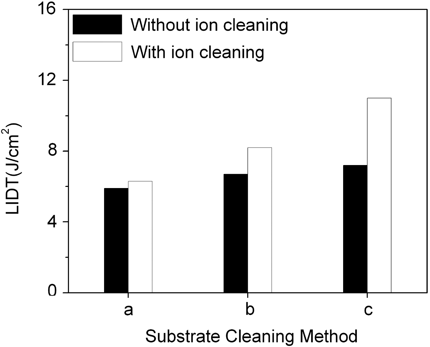
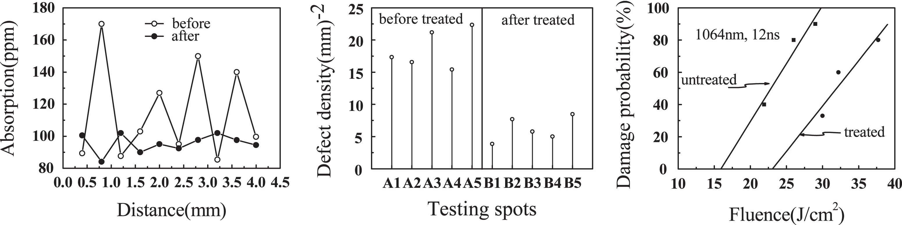
To remove the organic or particulate residue on the surface of the substrate, the substrate cleaning process must be thoroughly investigated. Three different methods, namely manually swabbing with lint-free wipes immersed in an organic solvent, ultrasonic cleaning, and acid solvent etching, were used to clean the substrate. The cleaning effect was evaluated with the AFM technique, as shown in Figure 5. The results show that cleaning with acid solvent is the most efficient way to remove the surface defects, while organic solvent swabbing is the worst. Then, the second harmonic antireflection coatings were deposited on substrates cleaned by the above methods, and the laser resistance was evaluated with a measurement facility developed in our group according to ISO21254[10]. The results show that the more the surface defects are removed, the higher the damage threshold value that is yielded, as shown in Figure 6.
Figure 5. Surface morphology of BK7 glass cleaned by different methods examined by an AFM: (a) manually swabbing with lint-free wipes, (b) ultrasonic cleaning, (c) acid solvent etching.
Figure 6. LIDT of antireflection coating with different cleaning methods (532 nm,  ${0}^{\circ } $, 10 ns).
Contaminants from the fixtures to hold the substrate and the vacuum chamber walls can also contribute to contamination of the substrate to be coated. Therefore, plasma ion cleaning is introduced to remove the surface contaminants of the substrate in a vacuum chamber before deposition. The LIDT results are also shown in Figure 6. It can be seen that the plasma ion cleaning process can efficiently improve the LIDT of the second harmonic antireflection coating.
Deposition technique
With the development of a deposition technique, there are many methods available for deposition of a coating, such as electron-beam evaporation, ion-beam sputtering, and magnetron sputtering. Although electron-beam evaporation coatings have the disadvantages of scattering and humidity-related spectral and stress shifts due to the columnar microstructure of the films, it is still the most widely researched deposition technique for laser coating at  $1\omega $ in the nanoscale pulse length regime. Besides laser-resistant source materials (
 ${\mathrm{HfO} }_{2} $ and
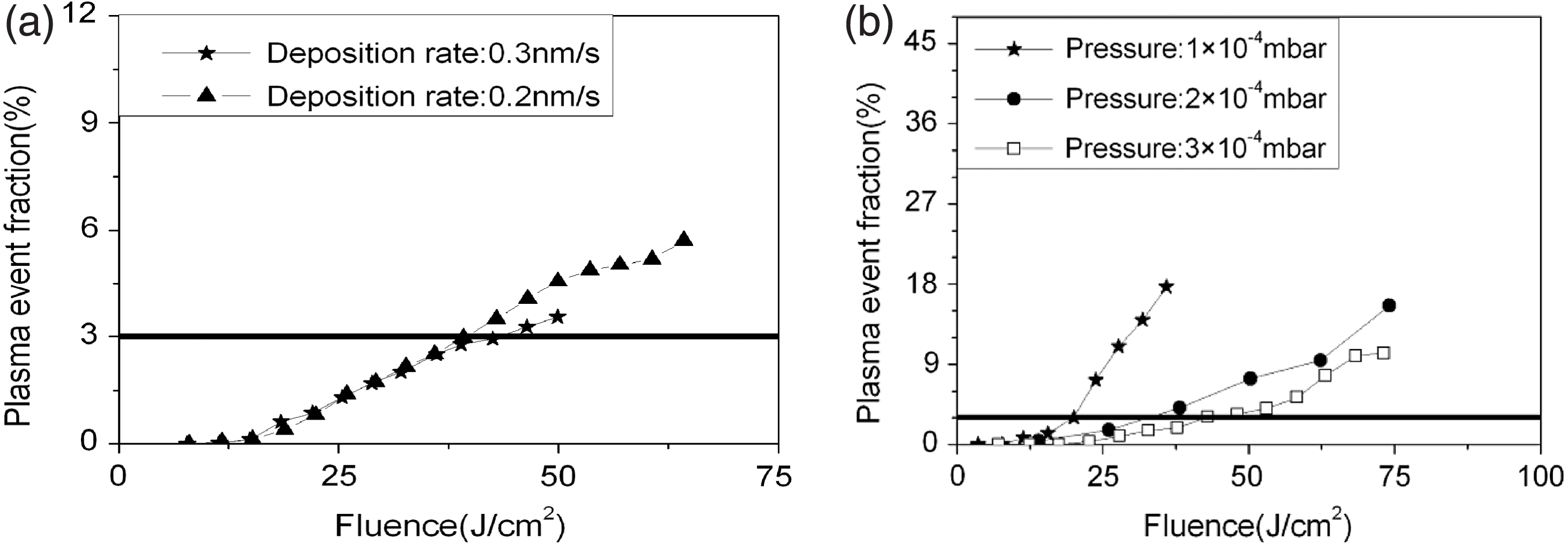
  ${\mathrm{SiO} }_{2} $), many parameters play great roles in the deposition of a high-power laser coating, including the deposition rate, substrate temperature, vacuum pump type, oxygen partial pressure, pre-melting process, and electron-gun sweep. Generally, the stoichiometry of the growing film depends on the rate of deposition, substrate temperature, and oxygen partial pressure, and significantly affects the intrinsic damage behavior. These parameters must be optimized to produce a homogeneous layer with the desired contents and structure. The effect of deposition rate and oxygen partial pressure on the damage behavior of mirror was investigated, as shown in Figure 7. The experimental results show that a relatively higher oxygen flow and lower deposition rate will benefit the coating oxidization, and thus have a positive impact on the laser-induced damage threshold.
Figure 7. Optimization of deposition process.
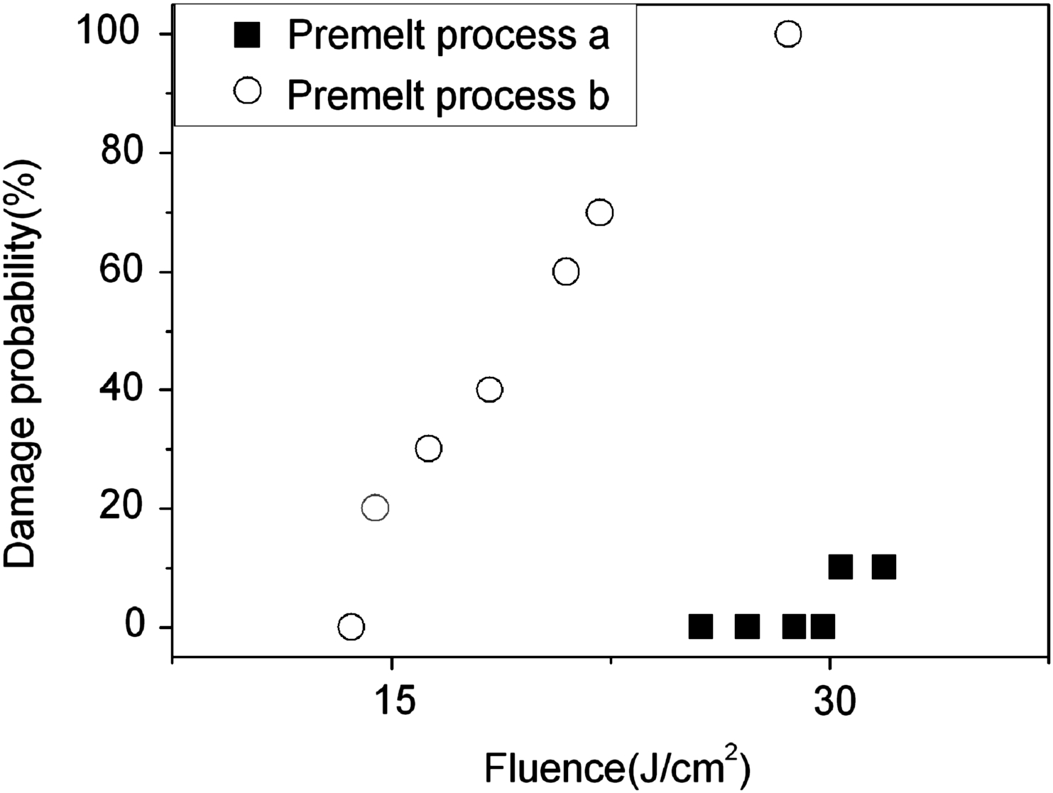
Besides the intrinsic absorption of non-stoichiometric material, one must strictly control the involvement of defects during the deposition process. The ejection of coating material is also an important source of nodular defects. For the high-index material, optimizing the pre-melting process of the source material is efficient in suppressing the material ejection. Figure 8 shows the measured LIDT of high-reflectance coatings with different pre-melting processes. It can be seen that optimization of the pre-melting process may rapidly decrease the probability of damage to the coating.
Figure 8. Measured LIDT of high-reflectance coating with different pre-melting processes.
Post treatment
Although optimization of the deposition process can decrease the defect density and improve the stoichiometry of coatings, it is difficult to get a perfect coating with no defects and good stoichiometry. Post treatment is another effective technique to improve the LIDT of the coating, including post annealing and laser conditioning, as well as post-plasma treatment.
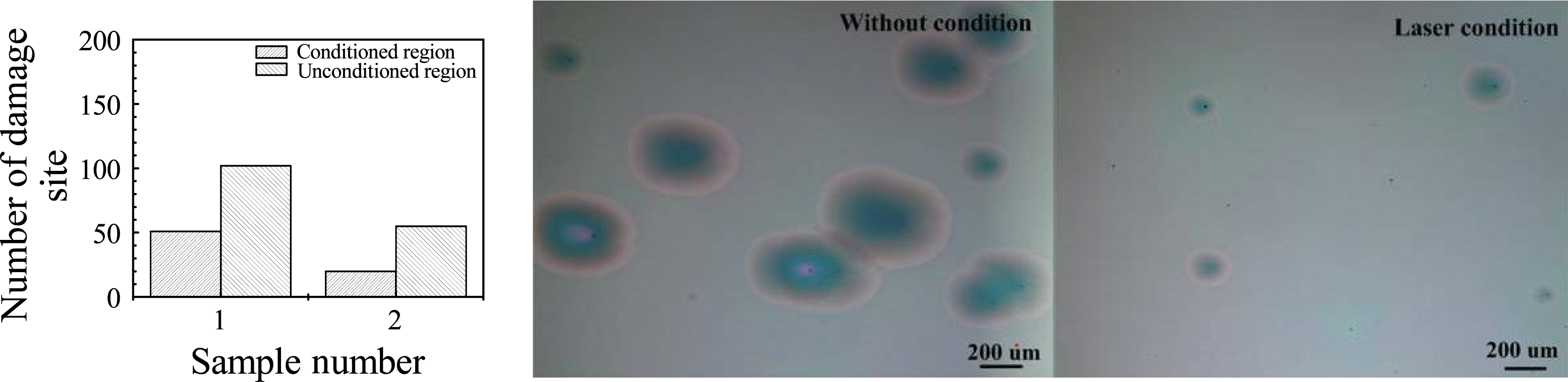
Laser conditioning is the process where the sample is irradiated at low fluence and then ramped in fluence until the sample has been exposed to the peak operating fluence[Reference Stolz, Sheehan, Maricle, Schwartz, Hue, Exarhos, Guenther, Kozlowski, Lewis and Soileau11]. A laser conditioning platform was built in our group, and the laser conditioning of the  $1\omega $ HR coatings was investigated on this platform, as shown in Figure 9. It is clear that laser conditioning could effectively reduce the number and size of the plasma scalds, and consequently increase the functional LIDT of the coating.
Figure 9. Number of damage site and damage morphology without and with laser conditioning.
 ${\mathrm{ZrO} }_{2} $ single-layer coatings were deposited to investigate the effect of the post-plasma treatment. The results show that post-plasma treatment reduces the average micro-defect density and film absorption, which consequently increases the LIDT of the single-layer coating, as shown in Figure 10[Reference Zhang, Shao, Zhang, Fan, Tan and Fan12,Reference Zhang, Wang, Fan, Cai, Zheng, Shao and Fan13] .
Figure 10. Absorption, defect density, and LIDT of  ${\mathrm{ZrO} }_{2} $ coating with and without post-plasma treatment.
Electric field distribution
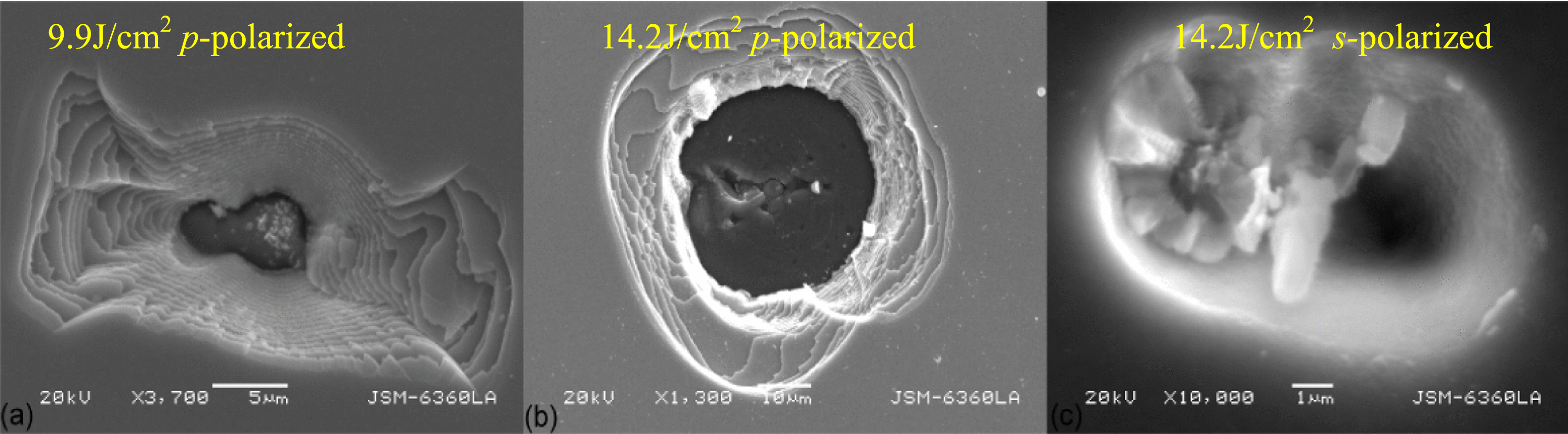
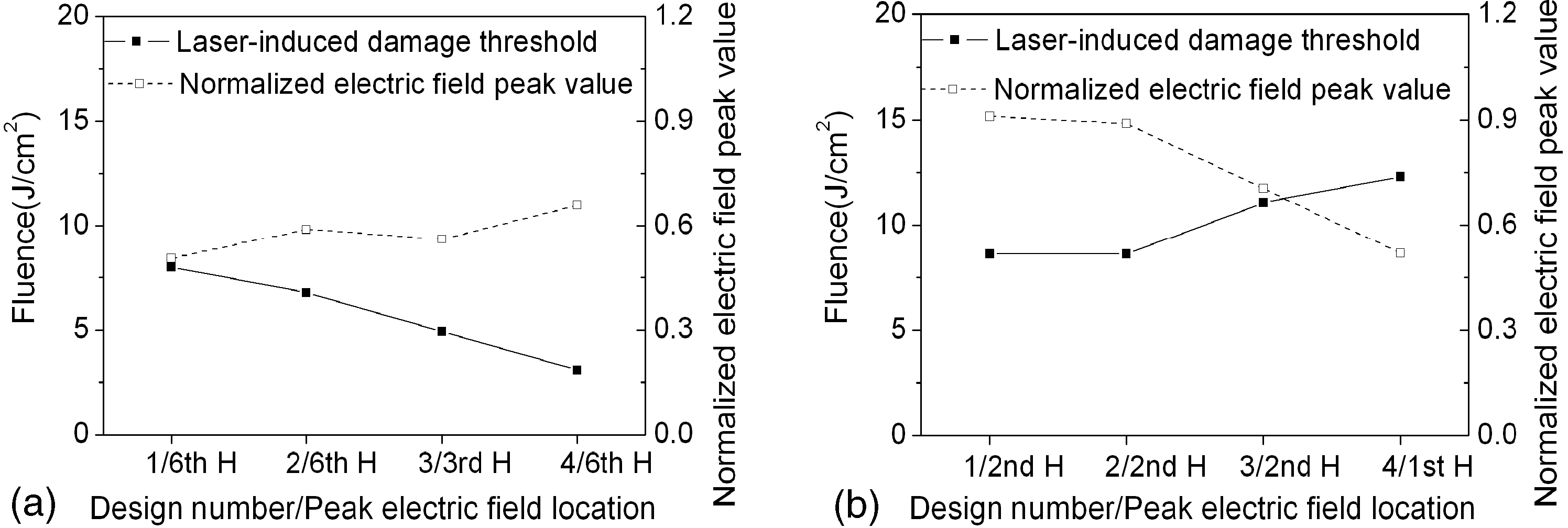
Optimization of the electric field distribution could minimize the negative effects of intrinsic and defect absorption in coatings. Four kinds of polarizer were designed and prepared with the same process conditions. The typical damage morphology is pits induced by nodular defects, which can be examined with a scanning electron microscope (SEM), as shown in Figure 11. Besides, measurements of the defect density and absorption show similar results for all kinds of polarizer. The main difference between the four kinds of polarizer is the electric field distribution. The dependence of the LIDT on the peak electric field is shown in Figure 12. For both p-polarized and s-polarized light, the lower the electric field peak intensity, the higher the laser-induced damage threshold.
Figure 11. Typical damage morphology with a fluence of  $9. 9~\mathrm{J} / {\mathrm{cm} }^{2} $ (p-polarized wave),
  $14. 2~\mathrm{J} / {\mathrm{cm} }^{2} $ (p- and s-polarized waves).
Figure 12. LIDT versus peak electric field for four kinds of polarizer: (a) p-polarized wave, (b) s-polarized wave.
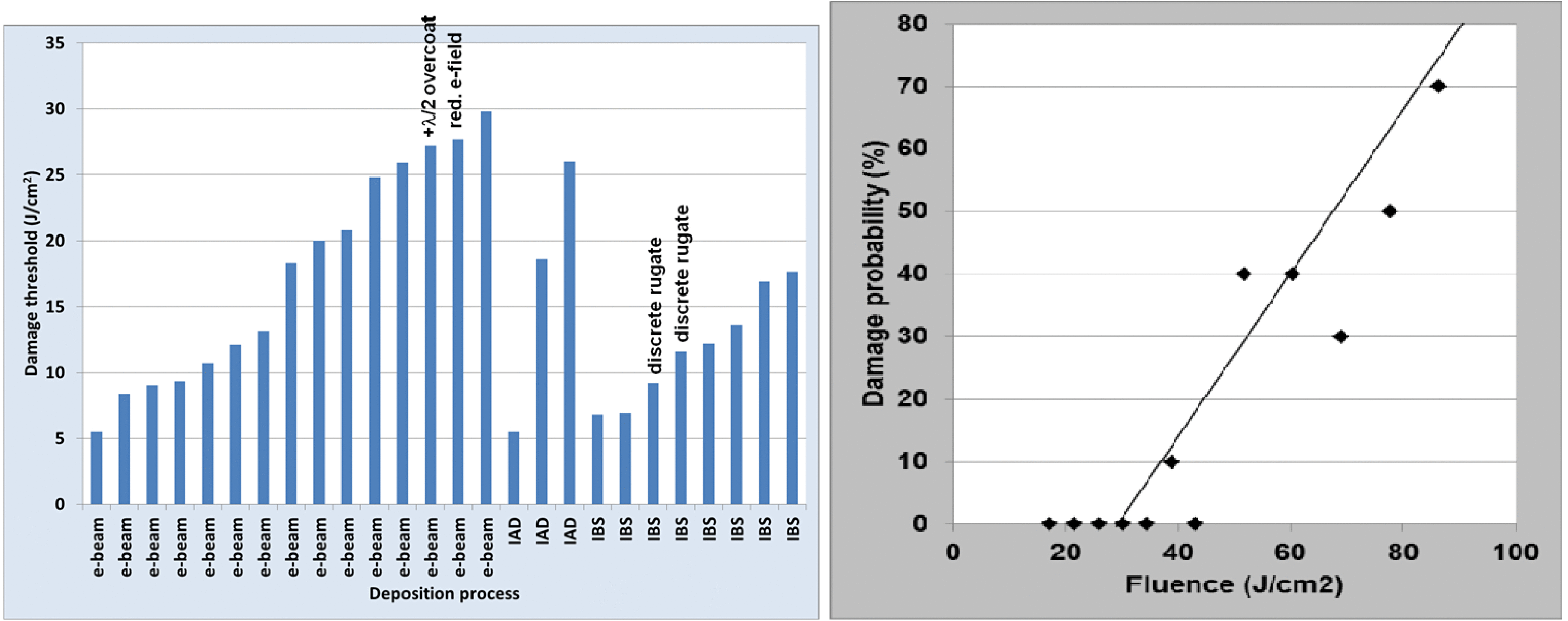
With the optimizing field design (electric field, temperature field, and stress field) and deposition process, a polarizer beam splitter was prepared and submitted to take part in the 2012 damage competition of the XLIV Annual Boulder Damage Symposium. The results of all 26 samples from different research groups in the competition are summarized in Figure 13. The polarizer submitted by our group showed the best result. The damage probability is also shown in Figure 13. No detective damage sites were observed when the laser fluence is less than  $34. 5~\mathrm{J} / {\mathrm{cm} }^{2} $ (1064 nm, 10 ns, p-polarized wave, and
  $56. {4}^{\circ } $). The damage threshold of zero probability is fitted to be
  $29. 8~\mathrm{J} / {\mathrm{cm} }^{2} $. With the optimizing design and process, the LIDT is above
  $60~\mathrm{J} / {\mathrm{cm} }^{2} $ (1064 nm, 3 ns) for the small-aperture pick-off mirror, and the LIDT is above
  $23~\mathrm{J} / {\mathrm{cm} }^{2} $ (1064 nm, 3 ns) and
  $14~\mathrm{J} / {\mathrm{cm} }^{2} $ (1064 nm, 3 ns) for the larger-aperture mirror and polarizer after laser conditioning.
Figure 13. LIDT of polarizer beam splitter for a p-polarized wave in the 2012 damage competition of XLIV Annual Boulder Damage Symposium[Reference Stolz, Exarhos, Gruzdev, Menapace, Ristau and Soileau14].
4. Stress and wavefront control of a coating
The coatings in an optical system can have a great effect on the beam quality, particularly the defocus and on-axis astigmatism. For a high-power laser facility, e.g. NIF and LMJ, hundreds of optical coating components were used in each beamline. Therefore, tight control of the wavefront aberrations is necessary to achieve high-quality focusable energy and power for producing extreme temperature and pressure.
As is well known, the wavefront of an optical coating depends on the figure and stress stability of the substrate, deposition parameters, uniformity of coating, post-treatment process, aging process, and application environment. Except for physical variance-induced wavefront aberrations, e.g., figure of substrate and uniformity of coating, wavefront aberrations are closely related to the stress in the substrate and the coating. Consequently, the preparation of non-wave-front aberration coatings is systematic engineering. One needs to thoroughly understand the material stress, and take effective measures to decouple all the factors. Finally, a series of scientific laws is used to control the wavefront of optical coating components.
Optimization of deposition parameters
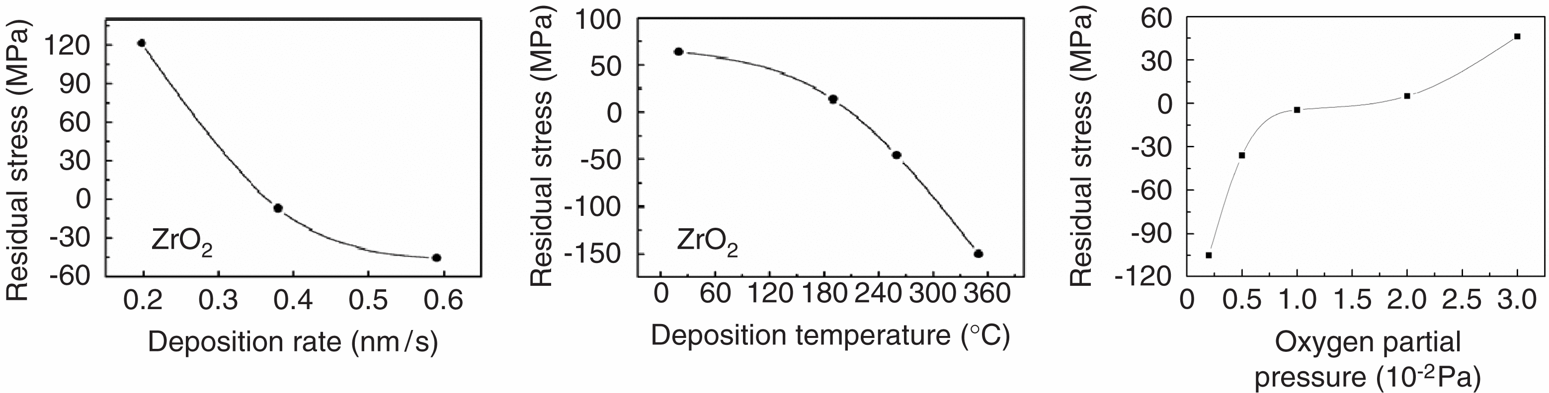
As mentioned above, the residual stress of a coating is sensitive to the deposition parameters, including the deposition temperature, deposition rate, and working pressure[Reference Shen, Shao, Yu, Fan, He and Shao15–Reference Shao, Fan, Shao and He17], as shown in Figure 14. On the one hand, the residual stress can be tuned from tensile stress to compressive stress by adjusting the deposition parameters; on the other hand, the balance of compressive and tensile stress between alternative high and low refractive index material can yield a stress-free optical coating[Reference Shao, Shao, He and Fan18].
Figure 14. Dependence of residual stress of the coating on the deposition parameters.
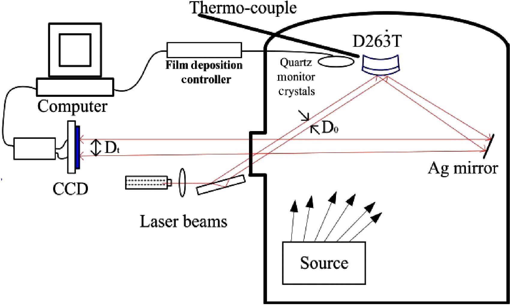
In situ stress measurement
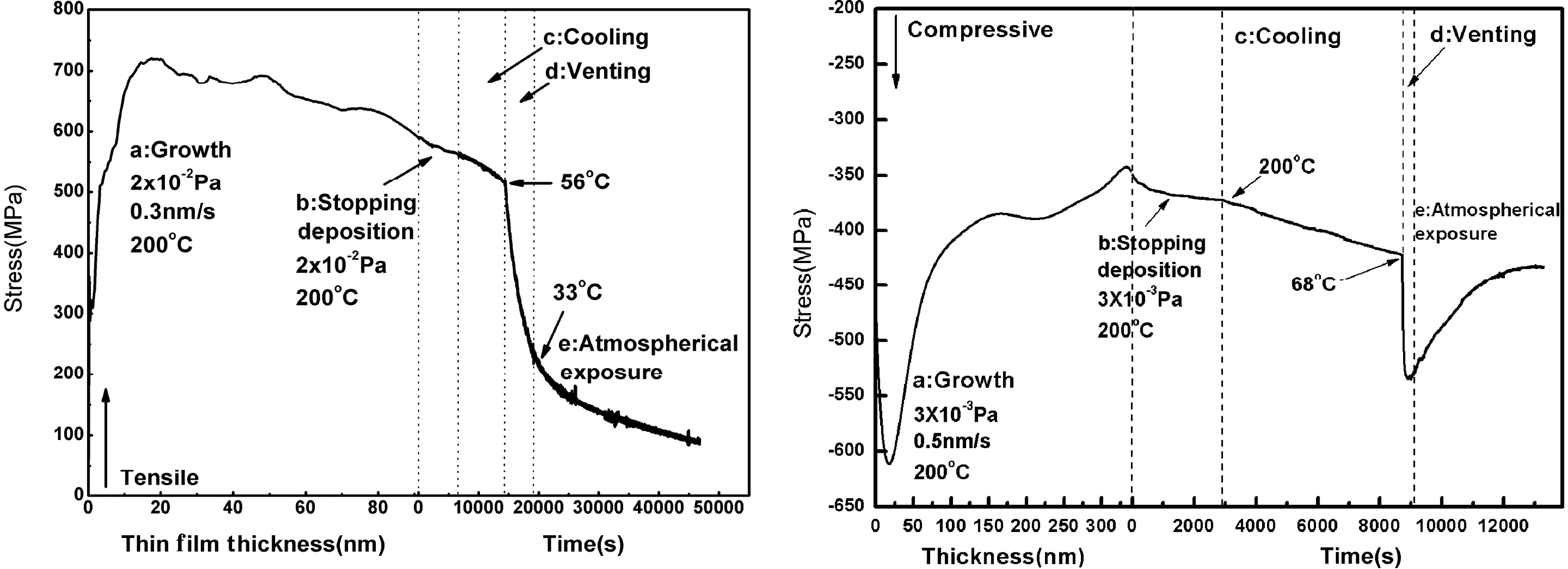
Recording of the residual stress evolution could afford detailed information for the investigation of the stress mechanism during the deposition process of a coating. An in situ stress measurement apparatus has been developed in our group, based on wafer curvature measurement by optical deflection of two parallel light beams. A schematic diagram of the in situ stress measurement system is shown in Figure 15. The typical stress evolution curve of the  ${\mathrm{HfO} }_{2} $ and
  ${\mathrm{SiO} }_{2} $ monolayer is plotted in Figure 16[Reference Fang, Hu and Shao19]. The stress evolution of the coating is clearly shown for five sub-procedures: thin film deposition, stopping deposition, cooling, venting, and exposure. With the stress-matching technique, the reflected wavefront is less than
 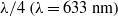 $\lambda / 4~(\lambda = 633~\mathrm{nm} )$ for the small-aperture mirror, and less than
 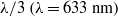 $\lambda / 3~(\lambda = 633~\mathrm{nm} )$ for the larger-aperture mirror and polarizer at the used angle in our group.
Figure 15. Schematic diagram of the in situ stress measurement system.
Figure 16. Typical stress evolution curve of  ${\mathrm{HfO} }_{2} $ and
  ${\mathrm{SiO} }_{2} $ films recorded with the in situ stress measurement system.
5. Summary
In order to meet the stringent performance requirements of laser coatings, the defects and stress are strictly controlled during the deposition of an optical coating. The deposited optical coating can meet the requirement of laser resistance and wavefront aberration in the series SG laser facility with the developed manufacturing process.
Acknowledgements
The authors would like to acknowledge Prof. Zhengxiu Fan for useful discussions and support in preparing this manuscript. The authors would also like to acknowledge the damage testing, reflected wavefront measurements, and spectral characterization performed by Yuan’an Zhao, Dawei Li, Qiling Xiao, Guohang Hu, and Xiaofeng Liu.

 Open access