Hostname: page-component-848d4c4894-x5gtn Total loading time: 0 Render date: 2024-06-06T07:37:49.664Z Has data issue: false hasContentIssue false

Micro-Raman characterization of Ge diffusion and Si stress change in thin epitaxial Si1−xGex layers on Si(100) after rapid thermal annealing

Published online by Cambridge University Press:  03 April 2012

Chun-Wei Chang
Affiliation:
Taiwan Semiconductor Manufacturing Company, Ltd., Hsinchu, Taiwan 300-77, Republic of China
Min-Hao Hong
Affiliation:
Taiwan Semiconductor Manufacturing Company, Ltd., Hsinchu, Taiwan 300-77, Republic of China
Wei-Fan Lee
Affiliation:
Taiwan Semiconductor Manufacturing Company, Ltd., Hsinchu, Taiwan 300-77, Republic of China
Kuan-Ching Lee
Affiliation:
Taiwan Semiconductor Manufacturing Company, Ltd., Hsinchu, Taiwan 300-77, Republic of China
Li-De Tseng
Affiliation:
Taiwan Semiconductor Manufacturing Company, Ltd., Hsinchu, Taiwan 300-77, Republic of China
Yi-Hann Chen
Affiliation:
Taiwan Semiconductor Manufacturing Company, Ltd., Hsinchu, Taiwan 300-77, Republic of China
Yen Chuang
Affiliation:
Taiwan Semiconductor Manufacturing Company, Ltd., Hsinchu, Taiwan 300-77, Republic of China
Yu-Ta Fan
Affiliation:
Taiwan Semiconductor Manufacturing Company, Ltd., Hsinchu, Taiwan 300-77, Republic of China
Takeshi Ueda
Affiliation:
WaferMasters, Inc., San Jose, California 95112
Toshikazu Ishigaki
Affiliation:
WaferMasters, Inc., San Jose, California 95112
Kitaek Kang
Affiliation:
WaferMasters, Inc., San Jose, California 95112
Woo Sik Yoo*
Affiliation:
WaferMasters, Inc., San Jose, California 95112
*
a)Address all correspondence to this author. e-mail: woosik.yoo@wafermasters.com
Get access

Abstract

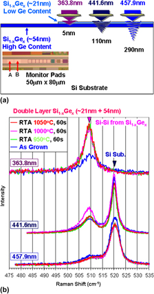
Boron-doped, single (∼54 nm) or double (∼21 + 54 nm) Si1−xGex layers were epitaxially grown on 300-mm-diameter p-Si(100) device wafers with 20 nm technology node design features, by ultrahigh vacuum chemical vapor deposition. The Si1−xGex/Si wafers were annealed in the temperature range of 950–1050 °C for 60 s to investigate the effect of annealing on possible changes of Ge content and Si stress near the Si1−xGex/Si interface. High spectral resolution, micro-Raman spectroscopy was used as a nondestructive characterization technique with five excitation wavelengths of 363.8, 441.6, 457.9, 488.0, and 514.5 nm. Ge diffusion and generation of compressive stress at the Si1−xGex/Si interface were measured on all annealed wafers. Ge diffusion and the accumulation of compressive Si stress after annealing showed significantly different behaviors between single- and double-layer Si1−xGex/Si wafers. Raman characterization results were compared with secondary ion mass spectroscopy and high-resolution x-ray diffraction results.

Type
Articles
Copyright
Copyright © Materials Research Society 2012

Access options

Get access to the full version of this content by using one of the access options below. (Log in options will check for institutional or personal access. Content may require purchase if you do not have access.)

References

REFERENCES

1.Dennard, R.H., Gaensslen, F.H., Yu, H.N., Leo Rideout, V., Bassous, E., and Leblanc, A.R.: Design of ion-implanted MOSFET’s with very small physical dimensions. IEEE J. Solid State Circuits, 9, 256 (1974); Proceedings of the IEEE, 87(4), 668(1999).Google Scholar
2.Fischetti, M.V.: Scaling MOSFETs to the limit: A physicist’s perspective. IBM Res. Rep. RC22828, 1 (2003).Google Scholar
3.Oberhuber, R., Zandler, G., and Vogl, P.: Subband structure and mobility of two-dimensional holes in strained Si/SiGe MOSFET’s. Phys. Rev. B 58, 9941 (1998).CrossRefGoogle Scholar
4.Mohta, N. and Thompson, S. E.: Mobility enhancement: The next vector to extend Moore’s law. IEEE Circuits Devices Mag. 21, 18 (2005).CrossRefGoogle Scholar
5.Thompson, S.E., Sun, G., Choi, Y.S., and Nishida, T.: Uniaxial-process-induced strained-Si: Extending the CMOS roadmap. IEEE Trans. Electron. Dev. 53(5), 1010 (2006).Google Scholar
6.Rim, K., Welser, J., Takagi, S., Hoyt, J.L., and Gibbons, J.F.: Enhanced hole mobilities in surface-channel strained-Si p-MOSFETs, in Proceedings of the IEEE IEDM Technical Digest, December 10–13, 1995, pp. 517520.Google Scholar
7.Reiche, M., Moutanabbir, O., Hoentschel, J., Gösele, U., Flachowsky, S., and Horstmann, M.: Strained silicon devices. Solid State Phenom. 156-158, 61 (2010).Google Scholar
8.Manasevit, H.M., Gergis, I.S., and Jones, A.B.: Electron mobility enhancement in epitaxial multilayer Si–Si1−xGex alloy films on (100) Si. Appl. Phys. Lett. 41(5), 464 (1982).Google Scholar
9.People, R., Bean, J.C., Lang, D.V., Sergent, A.M., Stormer, H.L., Wecht, K.W., Lynch, R.T., and Baldwin, K.: Modulation doping in GexSi1−x/Si strained layer heterostructures. Appl. Phys. Lett. 45(11), 1231 (1984).Google Scholar
10.Fischetti, M.V., Ren, Z., Solomon, P.M., Yang, M., and Rim, K.: Six-band k·p calculation of the hole mobility in silicon inversion layers: Dependence on surface orientation, strain, and silicon thickness. J Appl. Phys. 94(2), 1079 (2003).Google Scholar
11.Thompson, S.E., Armstrong, M., Auth, C., Cea, S., Chau, R., Glass, G., Hoffman, T., Klaus, J., Zhiyong, Ma, Mcintyre, B., Murthy, A., Obradovic, B., Shifren, L., Sivakumar, S., Tyagi, S., Ghani, T., Mistry, K., Bohr, M., and El-Mansy, Y.: A logic nanotechnology featuring strained silicon. IEEE Electron Device Lett. 25, 191 (2004).CrossRefGoogle Scholar
12.Zhang, D., Nguyen, B.Y., White, T., Goolsby, B., Nguyen, T., Dhandapani, V., Hildreth, J., Foisy, M., Adams, V., Shiho, Y., Thean, A., Theodore, D., Canonico, M., Zollner, S., Bagchi, S., Murphy, S., Rai, R., Jiang, J., Jahanbani, M., Noble, R., Zavala, M., Cotton, R., Eades, D., Parsons, S., Montgomery, P., Martinez, A., Winstead, B., Mendicino, M., Cheek, J., Liu, J., Grudowski, P., Ranami, N., Tomasini, P., Arena, C., Werkhoven, C., Kirby, H., Chang, C.H., Lin, C.T., Tuan, H.C., See, Y.C., Venkatesan, S., Kolagunta, V., Cave, N., and Mogab, J.: Embedded SiGe S/D PMOS on thin body SOI substrate with drive current enhancement, in Proceedings of the Symposium on VLSI Technology, June 14–16, 2005, pp. 2627.Google Scholar
13.Ouyang, Q., Yang, M., Holt, J., Panda, S., Chen, H., Utomo, H., Fischetti, M., Rovedo, N., Li, J., Klymko, N., Wildman, H., Kanarsky, T., Costrini, G., Fried, D.M., Bryant, A., Ott, J.A., Ieong, M., and C- Sung, Y.: Investigation of CMOS devices with embedded SiGe source/drain on hybrid orientation substrates, in Proceedings of the Symposium on VLSI Technology, June 14–16, 2005, pp. 2829.Google Scholar
14.Chau, R., Doczy, M., Doyle, B., Datta, S., Dewey, G., Kavalieros, J., Jin, B., Metz, M., Majumdar, A., and Radosavljević, M.: Advanced CMOS transistors in the nanotechnology era for high-performance, low-power logic applications, in Proceedings of Seventh International Conference on Solid-State and Integrated Circuit Technology (ICSICT, Shanghai, China, 2010), pp. 2630.Google Scholar
15.De Wolf, I.: Micro-Raman spectroscopy to study local mechanical stress in silicon integrated circuits. Semicond. Sci. Technol. 11, 139 (1996).Google Scholar
16.De Wolf, I.: Raman spectroscopy: About chips and stress. Spectrosc. Eur. 15(2), 6 (2003).Google Scholar
17.Alonso, M.I. and Winer, K.: Raman spectra of c-Si1-xGex alloys. Phys. Rev. B 39(14), 10056 (1989).Google Scholar
18.Zhao, L., Zuo, Y., Cheng, B., Yu, J., and Wang, Q.: Comparison between double crystals x-ray diffraction and micro-Raman measurement on composition determination of high Ge content Si1-xGex layer epitaxied on Si substrate. J. Mater. Sci. Technol. 22(5), 651 (2006).Google Scholar
19.Tzeng, Y.F., Ku, S., Chang, S., Yang, C.M., Chern, C.S., Lin, J., Hasuike, N., Harima, H., Ueda, T., Ishigaki, T., Kang, K., and Yoo, W.S.: Non-contact in-line monitoring of boron concentration from ultrathin boron-doped epitaxial Si1-xGex layers on Si(100) by multiwavelength micro-Raman spectroscopy. J. Mater. Res. 26(6), 739 (2011).Google Scholar
20.Tzeng, Y.F., Ku, S., Chang, S., Yang, C.M., Chern, C.S., Lin, J., Hasuike, N., Harima, H., Ueda, T., Ishigaki, T., Kang, K., and Yoo, W.S.: Non-contact in-line monitoring of Ge content and thickness variations of epitaxial Si1-xGex layers on Si (100) using polychromator-based multi-wavelength micro Raman spectroscopy. Appl. Phys. Express 3, 106601 (2010).Google Scholar
21.Yoo, W.S., Ueda, T., Ishigaki, T., and Kang, K.: Non-contact, non-destructive characterization of Ge content and SiGe layer thickness using multi-wavelength Raman spectroscopy, in Proceedings of the 17th IEEE International Conference on Advanced Thermal Processing of Semiconductors (RTP 2009, Albany, NY, September 2009), p. 169.Google Scholar
22.Yoo, W.S., Ueda, T., and Kang, K.: Characterization of uni-axially stressed Si and Ge concentration in Si1-xGex using polychromator-based multi-wavelength Raman spectroscopy. Ext. Abstr., in Proceedings of the Ninth International Workshop on Junction Technology (IWJT 2009, Kyoto, Japan, June 2009), p. 79.Google Scholar
23.Yoo, W.S., Ueda, T., Ishigaki, T., and Kang, K.: Non-destructive characterization of Ge content and Ge depth profile variations in Si1-xGex/Si by multi-wavelength Raman spectroscopy. ECS Trans. 28(1), 253 (2010).Google Scholar
24.Yoo, W.S., Ueda, T., Ishigaki, T., and Kang, K.: Non-contact and non-destructive measurement of Ge and B content in Si1-xGex/Si using very high resolution multi-wavelength Raman spectroscopy. ECS Trans. 33(6), 877 (2010).Google Scholar
25.Vartanian, V., Ueda, T., Ishigaki, T., Kang, K., and Yoo, W.S.: Evaluation of very high resolution multi-wavelength Raman spectroscopy for in-line characterization of patterned epitaxial Si1-xGex layers on Si(100) wafers. ECS Trans. 35(2), 205 (2011).Google Scholar
26.Yoo, W.S., Kang, K., Ueda, T., and Ishigaki, T.: Design of multi-wavelength micro Raman spectroscopy system and its semiconductor stress depth profiling applications. Appl. Phys. Express 2, 116502 (2009).Google Scholar
27.Yoo, W.S., Ueda, T., and Kang, K.: Stress depth profiling of silicon from nickel/silicon interface before and after silicide formation using polychromator-based multi-wavelength Raman spectroscopy. Ext. Abstr., in Proceedings of the International Conference on Solid State Devices and Materials (Tsukuba, Japan, September 2008), p. 376.Google Scholar
28.Trigg, A.D., Yu, L.H., Cheng, C.K., Kumar, R., Kwong, D.L., Ueda, T., Ishigaki, T., Kang, K., and Yoo, W.S.: Three dimensional stress mapping of silicon surrounded by copper filled through silicon vias using polychromator-based multi-wavelength micro Raman spectroscopy. Appl. Phys. Express 3, 086601 (2010).Google Scholar
29.Kwon, W.S., Alastair, D.T., Teo, K.H., Gao, S., Ueda, T., Ishigaki, T., Kang, K.T., and Yoo, W.S.: Stress evolution in surrounding silicon of Cu-filled through-silicon via undergoing thermal annealing by multiwavelength micro-Raman spectroscopy. Appl. Phys. Lett. 98, 232106 (2011).CrossRefGoogle Scholar
30.Chang, C.W., Hong, M.H., Lee, W.F., Jang Jian, S.K., Chuang, Y., Fan, Y.T., Hasuike, N., Harima, H., Ueda, T., Ishigaki, T., Kang, K., and Yoo, W.S.: Contactless monitoring of Ge content and B concentration in ultrathin single and double layer Si1-xGex epitaxial films using multiwavelength micro-Raman spectroscopy. AIP Adv. 2, 012124 (2012).CrossRefGoogle Scholar
31.Fahey, P.M., Griffin, P.B., and Plummer, J.D.: Point defects and dopant diffusion in silicon. Rev. Mod. Phys. 61, 289 (1989).CrossRefGoogle Scholar
32.Moriya, N., Feldman, L.C., Luftman, H.S., King, C.A., Bevk, J., and Freer, B.: Boron diffusion in strained Si1-xGex epitaxial layers. Phys. Rev. Lett. 71(6), 883 (1993).CrossRefGoogle ScholarPubMed
33.Haddara, Y.M., Folmer, B.T., Law, M.E., and Buyuklimanli, T.: Accurate measurements of the intrinsic diffusivities of boron and phosphorus in silicon. Appl. Phys. Lett. 77(13), 1976 (2000).Google Scholar
34.Christensen, J.S.: Dopant diffusion in Si and SiGe. (Ph D Thesis, (KTH Royal Institute of Technology, Stockholm, Sweden, 2004).Google Scholar
35.Hikavyy, A., Nguyen, N.D., Loo, R., Ryan, P., Wormington, M., and Hopkins, J.: In-line characterization of pMOS devices with embedded SiGe and hetero bipolar transistor base layers by high-resolution x-ray diffraction, in Fourth International SiGe Technology and Device Meeting (ISTDM, Hsinchu, Taiwan, May 2008), Mon-P1–05.Google Scholar