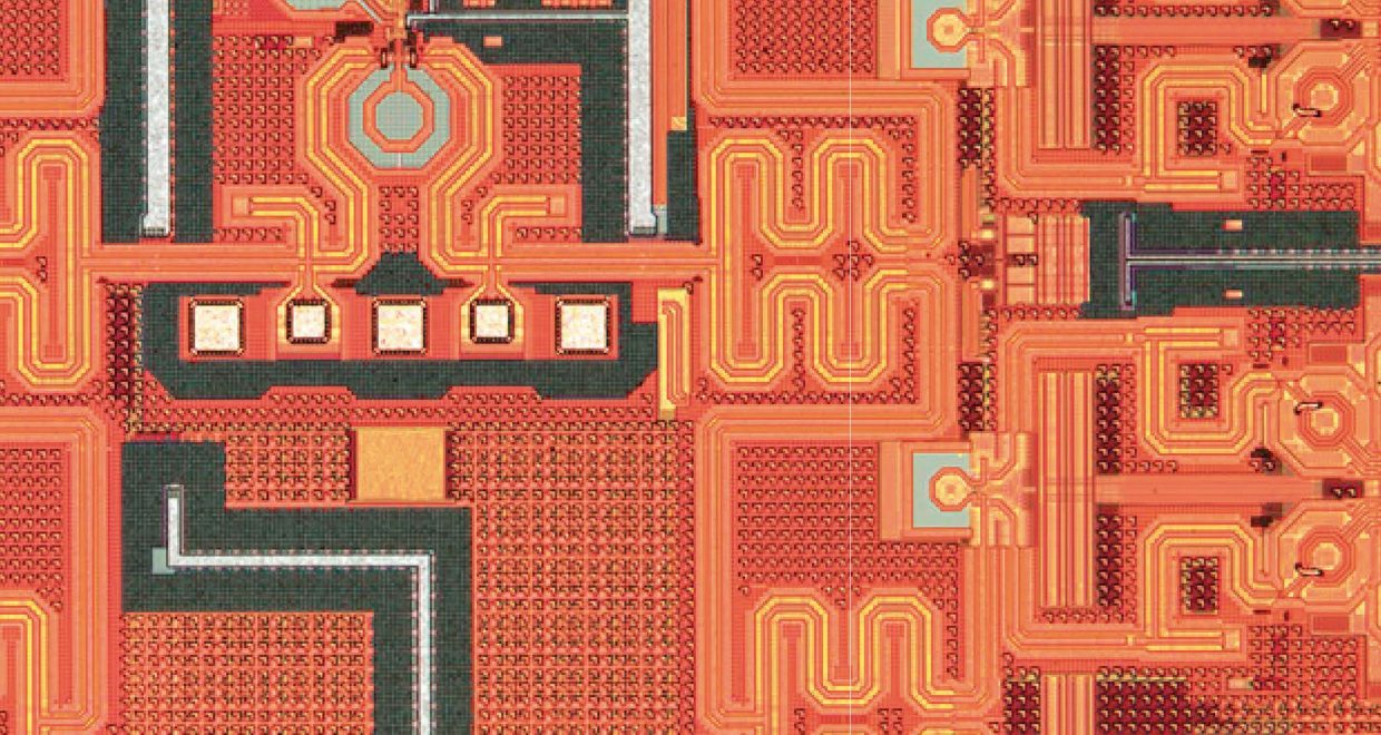
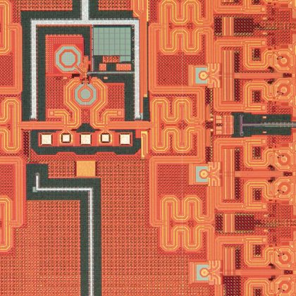
mm-Wave Research in Nanoscale Communication Integrated Circuits (NCIC) Labs
My involvement as one of the contributing authors [Millimeter-Wave Circuits for 5G and Radar] started with an interaction with Gernot Hueber during my presentation at a workshop in the 2017 International Microwave Symposium. He stated that he and Ali Niknejad have been thinking about publishing a book on millimeter-wave integrated circuits design for 5G. To have a timely impact on this rapidly growing field, they envisioned this book to be a series of editorial articles where experts in the field contribute articles about various aspects of the entire 5G communication systems from top architecture level all the way down block and transistor level implementations. He unofficially asked me whether I would be interested in joining the team. I was obviously intrigued to be part of this team, as there was no question in my mind that Ali and Gernot will be doing a great job in terms of organizing an effort to create the first book on millimeter-wave circuits for 5G applications.
I have been involved in the design of high frequency integrated circuits design since 2000. The NCIC Labs under my supervision currently conduct research in two areas, namely, (1) silicon-based RF/millimeter-wave/terahertz integrated circuits design for imaging, sensing, and wireless communications, and (2) ultra-low power electronics for brain-computer interface (BCI) systems.
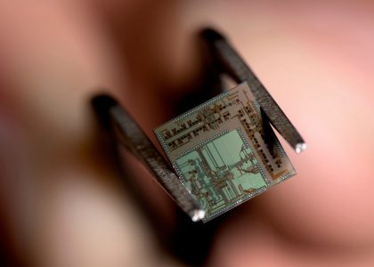
Research on the design and implementation of mm-wave building blocks and integrated systems in silicon technologies started way before the rise of 5G. Research institutions such as UC Berkeley, Caltech, our group at UC-Irvine, and etc. started flirting with the idea of designing high frequency and wideband circuits in silicon technologies in early 2000’s. The mere excitement of pushing the envelope to use silicon platform rather than advanced III-V semiconductors to design above 20-GHz circuits was the main driving force behind these early-day research activities in circuit design community. The successful demonstration of high frequency circuits in silicon with performance comparable to other expensive processes very soon gave rise to the possibility of designing the entire transceivers operating at mm-wave frequency range. There was appealing practical justifications for this effort than just a scientific experimentation:
According to Shannon theory, the channel capacity is directly proportional to communication bandwidth. On the other hand, wide untapped bandwidth is available at mm-wave frequency range. Wider bandwidth generally corresponds to higher data rate, an option that any wireless user would like to have. Furthermore, silicon implementation of the mm-wave transceivers brings forth the possibility of integrating the mm-wave front-end with mixed-signal and baseband backend. This was indeed a welcoming news, as the entire transceiver system could be implemented in a smaller chip real-estate. An equally important notion was that sophisticated signal processing techniques can be utilized to improve performance of mm-wave front-end circuits. Besides the aforementioned attributes, operation at higher frequencies presents yet another interesting advantage. Passive structures’ footprint scales down at higher frequencies. This includes the antenna structures, as well. The scaling of antenna size has opened up another great possibility of implementing multi-antenna architectures with large antenna elements. These multi-antenna architectures are currently being adopted for both base stations and small cells to combat inevitable path-loss at mm-wave frequencies and achieve higher capacity and co-channel user service. Increasing the number of antennas results in channel hardening and reduction of small- scale fading (less multi-path and Doppler spread), which in return simplifies baseband signal processing algorithms. Various configurations of multi-antenna architectures provide: (1) multiplexing gain to enhance link capacity through concurrent transmission of parallel data/user streams, (2) diversity gain to improve reliability of wireless links especially in non line-of-sight (NLOS) scenarios through transmission of copies of the same data stream, (3) antenna gain to combat ever increasing path loss at mm-wave frequencies, integrated wide-band noise, and co-channel interference through beamforming in LOS or directed NLOS scenarios. Operation at mm-wave frequencies also makes it possible to efficiently perform part of the multi-signal processing in the RF domain as opposed to a fully digital beamforming. Along this point of view, we recently investigated the idea of a partially-overlapped beamforming multi-input-multi-output (MIMO) architecture with simultaneous beamforming and MIMO capabilities both implemented in the RF domain capable of achieving higher beamforming and spatial multiplexing gains with lower number of elements compared to conventional architectures.

Moving along, the need for wider bandwidth and higher data rates will continue as new applications will be made available, and along with it, different types of challenges will arise. In particular, the availability of wide bandwidth within the high-side of mm-wave (called high-mmWave) frequency range from 100- to 300-GHz seems to partially address a challenging requirement associated with “conventional” wireless links, that is, the need for very complex modulation schemes (e.g., 1024QAM) at lower RF frequencies (i.e., ≤10 GHz) to achieve high data-rates. For instance, a simple binary phase-shift keying (BPSK) modulation of a base-band signal with a 10 GHz of RF bandwidth over a 100 GHz carrier frequency can potentially facilitate 5 Gbps line-of-sight wireless communication. In fact, operation at high-mmWave carrier frequency allows for wide absolute RF bandwidth at a relatively small fractional bandwidth (e.g., ~10%), which is achievable by current silicon technologies. Despite the availability of wide bandwidth, to further improve spectral efficiency and data rate, higher order modulations than a simple BPSK still seem to be necessary. Especially, the integrated thermal noise over the wide bandwidth mandated by higher-speed low order modulation (e.g., BPSK) signals, would demand much higher transmit output power to maintain the link signal-to-noise ratio.
Modern wireless radios use a set of in-phase and quadrature data converters (i.e., analog-to-digital and digital-to-analog converters) and baseband filters to generate high-order (de-)modulation schemes. This can limit the data-rate due to insufficient resolution/dynamic-range of data converters when operating at speeds higher than 20 Gbps. Perhaps one of the most (if not the most) crucial questions now would be: what are the power efficient solutions for the data-converter and back-end digital sides to achieve data rates well above 10 Gbps? It seems that moving some of the signal processing, especially high-order modulation/demodulation, from digital domain back to RF (or analog), quite contrary to the common practice in traditional RF transceivers, can create a viable pathway for implementation of end-to-end transceivers targeting 20 Gbps and above. This, in turn, may generate quite a bit of excitement for RF system and circuit designers to explore new architectures that address future generations of transceivers operating beyond 5G.
Further Reading:
The Incoming New Era of 5G – Ali M. Niknejad
The Berkeley Tale of 5G – Ali M. Niknejad
