Introduction
AlN substrates are needed for high-power microwave devices based on group III nitride heterostructures and UV photodetectors. High-performance GaN-based microwave transistors and solar-blind photodetectors have already been demonstrated on sapphire and SiC substrates. AlN substrates are expected to improve device characteristics further due to close lattice- and thermal-match with GaN-based device structures, high thermal conductivity and good insulating properties. High quality AlN materials have been grown in thin layer form, but bulk growth of AlN is much more difficult technological task. Main methods to grow bulk AlN are sublimation [Reference Slack and McNelly1] and growth from a melt [Reference Dugger2]. Experimental AlN crystals of about 15 mm in diameter have been reported for laboratory development [Reference Schowalter3]; commercial AlN wafers are not available.
Recently, we have demonstrated high quality AlN materials grown by the HVPE method [Reference Melnik, Nikolaev, Stepanov, Nikitina, Babanin, Dmitriev and Kuznetsov4]. AlN layers about 0.5 μm thick were grown on 6H-SiC substrates. Cathodoluminescence of AlN was measured at room temperature revealing edge peak at photon energy of 5.9 eV. The minimum value of the full width at a half maximum (FWHM) of ω-scan x-ray rocking curve was about 120 arc sec. The value of the specific resistivity of AlN was found to be 1013 Ohm cm at 300 K and 108 Ohm cm at 700 K.
In this paper, we report on HVPE growth of thick (up to 1 mm) AlN layers.
Experimental Procedure and Results
AlN deposition experiments were carried out on the HVPE growth machine equipped with horizontal open-flow hot wall reactor and two-zone resistively heated furnace (Fig. 1). One zone is the source zone and another is the growth zone. The maximum growth zone temperature is 1200°C. Substrate temperature for AlN was varied from 900°C to 1200°C. In our HVPE processes, Ar serves as a carrier gas. Ammonia and HCl are supplied from gas tanks. A boat containing metallic Al was placed in Al source tube. Substrates were placed on quarts pedestal in the growth zone of the reactor. AlN layers were grown using a reaction between aluminum chloride and ammonia. Aluminum chloride gas was formed by reaction between metallic Al and HCl, and was transported from the source zone to the growth zone by Ar flow.

Figure 1. Schematic view of HVPE growth reactor.
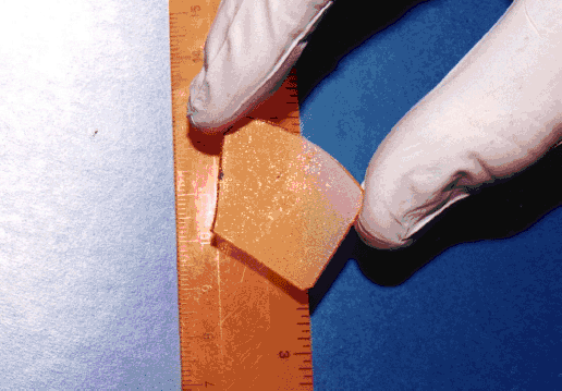
AlN layers up to 1 mm thick were grown by HVPE technique described above. Sapphire, SiC, and Si wafers were used as substrates. AlN growth rate was controlled in the range from 0.1 to 1 μm/min. After the growth, Si substrate was removed by chemical etching. Free-standing AlN wafers up to 3×3 cm2 in size were obtained (Fig. 2). The size of the wafer was equal to the size of the initial Si substrate. These are the largest AlN wafers reported to date. Results of material characterization of these AlN wafers are given bellow.

Figure 2. Photo of free-standing AlN wafer.
Fabricated AlN free-standing wafers were studied in terms of surface morphology, crystal structure, and optical properties. Top (as-grown) surface of AlN wafers contained growth pyramids (Fig. 3a). The back surface (former Si substrate – AlN interface) is flat and shiny. Usually, the back surface contained cracks (Fig. 3b). In order to use as-grown surface of AlN wafers for subsequent AlN or GaN epitaxy, this surface has to be polished.

Figure 3. Surface morphology of AlN free-standing wafer:
-
a) As-grown surface;
-
b) Former interface.
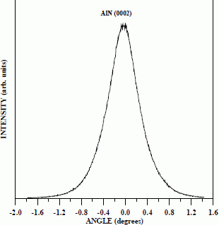
Crystal structure of free-standing AlN wafers was measured by x-ray diffraction. It was found that AlN has single crystal structure. X-ray diffraction scan measured in the range from 20 to 80 degrees showed only (0002) and (0004) AlN reflections indicating that the grown material has wurtzite structure and that the grown surface has (0001) orientation. X-ray rocking curves measured in ω–2Θ- and ω-scanning geometries had the FWHM values of about 100 arc sec and about 40 arc min, respectively (Fig. 4). Transmission electron microscopy study, which was done at Erlangen University, indicated that dislocation density in AlN wafers decreases from 109 – 1010 cm−2 in the former interface region down to 108 cm−2 in the surface region [Reference Albrecht, Strunk, Nikitina, Nikolaev, Melnik, Dmitriev and Vassilevski5].

Figure 4a. X-ray rocking curve measured at ω-scan for AlN free-standing wafer.

Figure 4b. X-ray rocking curve measured at ω-2Θ–scan for AlN free-standing wafer.
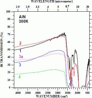
Optical properties of grown AlN was studied using cathodoluminescence and optical transmission (Fig. 5). Cathodoluminescence spectra contained two peaks, one at ∼375 nm (∼3.3 eV) and another at ∼207 nm (∼5.98 eV). The most intense peak at a wavelength of 375 nm is probably related to oxygen impurity. The edge peak at 207 nm is related to near band-gap optical transitions. The nature of both peaks must be investigated in a future.
We would like to mention that the fabricated AlN wafers were used as seeds for AlN sublimation bulk growth by sublimation [6] and no cracks have been observed in the bulk AlN materials.

Fig. 5. IR transmission spectra (300K) for free standing AlN samples:
-
1 - thickness is 0.05 mm, α = 17 cm−1;
-
2 - thickness is 0.08 mm, α = 20cm−1;
-
3 - thickness is 0.3 mm, α = 15 cm−1.
-
3a - thickness is 0.29 mm, α = 20 cm−1.
-
4 - thickness is 0.49 mm, α = 22 cm−1.
Conclusions
AlN wafers up to 3×3 cm2 in size were fabricated using HVPE technique. Thickness of AlN ranged from 0.05 to 1 mm. Lateral size of AlN wafers was equal to the size of initial substrates. Free-standing AlN wafers were fabricated employing Si substrate removal by chemical etching. It was found that AlN wafers are single crystals with 2H structure. Fabricated AlN wafers had (0001) orientation. The wafers exhibited edge luminescence at 5.9 eV and deep level luminescence peaking at 3.3eV (4 K). Future development will be focused on the fabrication of 2 inch diameter AlN substrates for group III nitride electronic devices.
Acknowledgements
We thank M. Albrecht and H. Strunk for TEM measurements, A. Davydov for x-ray measurements and J. Freitas for cathodoluminescence study of AlN samples. Work at Ioffe Institute and CGRC was partly supported by INTAS programs # 96-1031 and #96-2131. Work at TDI was partially supported by ONR (contract monitor Colin Wood).