Introduction
Since GaN is chemically stable and insoluble in all mineral acid and base solutions at room temperature [Reference Vartuli, Pearton, Abernathy, MacKenzie, Ren, Zolper and Shul1], most processing of III nitrides are currently done by dry plasma etching. High density plasma or energetic ion assisted etching were used to get a smooth etch surface and highly anisotropic sidewalls with high etch rates [Reference Shul, Howard, Pearton, Abernathy, Vartuli, Barnes and Bozack2-Reference Charles and Eddy4] . But there are several disadvantages to use dry etching, including generation of the ion-induced damage and difficulty in obtaining smooth etched sidewalls, which are required for the lasers cavity. The optical damage relative to yellow luminescence (YL) was also extensively investigated using photoluminescence spectroscopy on the etched surfaces. [Reference Chen, Pan and Chi5] The etching-induced damage will have detrimental effect on electronic or photonic device performance. Therefore, a reliable fabrication process producing low etch damage for GaN-based devices is necessitated.
Photoelectrochemical (PEC) etching is an alternative method to produce smooth surfaces and vertical sidewall facets without ion bombardment induced damages.[Reference Minskey, White and Hu6-Reference Youtsey, Adesida, Romano and Bulman8] As it is well-known that the yellow luminescence commonly existing in epitaxial grown GaN is related to the intrinsic defects or impurities. In this study, we used YL intensity variation to identify the etching-induced damages. A novel boiled KOH post treatment process was also developed to remove the etching-induced damages and achieve vertical and smooth facet sidewalls. A near damage-free etching process with vertical sidewalls and smooth etched surface can be realized by this post treatment process. This etching process could be applied to device fabrication such as laser cavity formation.
Experimental
The unintentionally-doped n-GaN samples (conc. < 5*1016 cm−3) used in this study were obtained from CREE Research, Inc. The thickness of nitride layer is 1.4 µm. Standard lift-off procedure was used to form the Ti metal mask that it is served as a contact for better photocurrent conduction. The GaN samples were sequentially cleaned by methanol and acetone and then rinsed with deionized water. A sample holder with two Teflon plates was used to fix the GaN samples. The PEC etching of GaN was carried out in a Teflon electrochemical cell containing an aqueous KOH electrolyte. The UV source was an Oriel high-pressure Hg-arc lamp, in which a water filter was mounted on the output window to remove infrared irradiation. The post-treatment was done with boiled KOH solution. For all photoluminescence (PL) measurements, a He-Cd laser (λ =325 nm) , typically operated at 1mW output power and focused to a spot with a diameter of 100 µm on the sample surface, was used as the excitation source. The luminescence was collected by a 50mm f/1.4 lens in the direction normal to the illuminated surface, and then focused into a SPEX 500M monochromator with an electrical-cooled GaAs photomultiplier. The etching profile was measured by HITACHI S-40000 FESEM.
Results and discussion
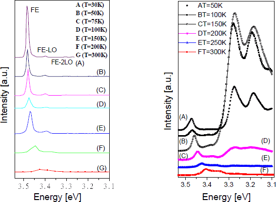
Our experimental results indicate that the etching rate is linearly proportional to the power density and it increases with increasing the KOH concentration. The relation of etching rate v.s. power density and KOH concentration is very similar to the published results [Reference Shul, Howard, Pearton, Abernathy, Vartuli, Barnes and Bozack2-Reference Charles and Eddy4]. Photoluminescence spectra corresponding to the etching condition with various UV power densities are shown in Figure 1, in which the 470W, 600W and 700W UV power corresponds to the power densities of 195 mW/cm2, 240 mW/cm2 and 290 mW/cm2 , respectively. All PL spectra are normalized to the same intensity scale of near-band-edge (NBE) peak at 364 nm. Spectrum A in Figure 1 shows the room temperature (R.T.) PL of the as-grown samples.

Figure 1. Defect induce yellow luminescence in PEC etching GaN with different UV power density

Figure 2. Temperature dependence photoluminescence of GaN (a) as- growth GaN with PL peaks as FE and phonon replica. (b)PEC etching GaN with PL peaks as FE, dislocation, DAP and phonon replica.
The peak at 364 nm (3.41 eV) is attributed to be the NBE emission and the 728 nm (1.705 eV) is the second harmonic counterpart. After etching with UV power density of 195 mW/cm2 in 0.02M KOH electrolyte, a yellow luminescence band centered at 563.6nm (2.2 eV) appeared (spectrum B). In spectrum C, the yellow luminescence band remained the same as in spectrum B while increasing the power density to 240 mW/cm2 . With the successive increase of the power density to 290 mW/cm2 for a longer etching, the very strong YL dominated and a dislocation-related peak at 370 nm (3.351 eV) emerged [Reference Hsieh, Hwang, Hung and Hwang9] as shown in spectrum D. This means that the etched GaN surfaces were seriously damaged such that the YL-related recombination centers were formed to annhilate the exciton-related luminescence due to trapping of excitons by the etching-induced defect traps. The YL relative to etching-induced damage will increase when etching GaN in the condition of higher power and/or longer time. To investigate origin of the etching-induced YL band emission, variable temperature PL measurements were done. Figure 2(a) shows the temperature-dependent PL of as-grown GaN samples. As were also observed by other authors, the free exciton (FE) peak position shifted to higher energy (blue shift) with decreasing temperature. The temperature coefficient of FE peak was determined to be 2.93×10⁻⁴ eV/K (100°K<T<300°K). Two regular LO-phonon replicas FE-LO and FE-2LO were observed in Figure 2(a) due to dominance of the polariton-phonon scattering at low temperature [Reference Kovalev, Averboukh, Volm and Meyer10]. After PEC etching of GaN with UV power density of 322 mW/cm2 and KOH concentration of 0.05M for 30 minute, the R.T. PL spectrum exhibited a new emission that is assigned to be donor-acceptor-pair (DAP) transition. The corresponding variable temperature PL spectra are shown in Figure 2(b). By successively decreasing the sample temperature to 200°K and below, an obvious enhancement of DAP emission was observed. Compared to the NBE transition, the peak position of DAP was less temperature-dependent [Reference Matsumoto and Aoki11] and was pinned at 3.229 eV. Moever, the photon from DAP transition can interact with the phonon to create the DAP-LO coupling with the gain or loss of one phonon energy. At temperature below 100 K, the LO phonon energy is about 91 meV that is consistent with the observation of the A1 (LO) mode (734.75 cm−1) in our FTIR measurement. In addition, we also found that the variation of YL intensity is connected to DAP emission intensity, that is, the YL intensity increased as the DAP emission intensity increased. This seems to imply that these two radiative recombination paths share the same electronic transition levels. In the following paragraph, we will dedicate to build a defect model to explain the observed phenomena in our experiments.

Figure 3. Damage remove by PEC etching GaN (a) low concentration of boil KOH with remove the damage layer produced YL in short time treatment. (b) high concentration on of boil KOH and low time treatment will create damage to GaN surface
In as-grown GaN film, a weak YL band exists too. It appears to have the same origin as the induced defects during PEC etching in our experiment. YL involves transitions from a deep state in the upper half of the gap either to the valence band, or to a (relatively) shallow acceptor. They are also termed as the shallow-donor to deep-acceptor transition and the deep donor-like to shallow-acceptor transition. The complex defect VGa-ON create a deep donor-like state (DD−) above the VBM about 2.2 eV. The excited carriers escape from the shallow donor states created by VN (Nitrogen vacancy) to DD− state in a nonradiative recombination process and then to a shallow acceptor with the YL emission (2.2 eV) [Reference Glaser, Kennedy, Doverspike, Rowland, Gaskill, Olson, Kuznia and Wickenden12]. Our results support this model and the induced defect during PEC etching process were suggested to be Ga vacancy bonds to oxygen in the nitrogen site. The possible reaction mechanism is as follows. The OH− coming from KOH electrolyte prefers to react with Ga rather than N to form gallium oxide that subsequently dissolves into the solution. A gallium vacancy will be therefore created to bond with the neighboring antisite defects arising from the occupation of nitrogen sites by the oxygen atoms. As seen from the temperature-dependent PL spectrum, a YL transition from DD− to a shallow acceptor level was identified. At low temperature, this transition was quenched. The excited carriers follow another recombination path from a shallow donor state to a shallow acceptor state, that is, the DAP transition. The YL intensity is strongly dependent on the amount of the acceptor states. The less the acceptor states, the weaker the YL intensity, and therefore the weaker then DAP peak intensity. This coincides with our results. From the above discussion, we would suggest that the defect is the defect complex of VGa-ON rather just VGa . Further support for the energy position assignment of the observed YL stems from the AES spectra.
The surface composition of as-growth with Ga:N (1.49:1) sample. From the PL of the etching surface with less YL, the surface composition of Ga:N (1.22:1) shown. While strong YL is created by PEC etching, the surface composition of Ga decreased with GaN (1.11:1). From the surface composition analysis, we can find that the surface gallium decreases while the YL intensity increases and the surface oxygen increases while YL intensity increases. This indicates that the YL intensity will increase as the concentration of VGa-ON defect complex increases.
The damaged layer induced by PEC etching of GaN was stable and can not be removed by the conventional chemical etching methods such as HCl:H2O (1:1), HF:H2O (1:1) or mixed solution at room temperature or elevated temperature. This can be confirmed from the PL measurement in which the YL band still exists after various chemical treatments as listed above. A novel skill with a post-treatment process in boiled KOH solution was evaluated for damage removed. In Figure 3(a), the PL spectrum from as-grown GaN samples was shown. No YL band is found on the as-grown samples. After PEC etching with power density of 186 mW/cm2 and KOH concentration of 0.02M, the defect complex VGa-ON relative to YL was present. After 1M boiled KOH post-treatment for 10 minutes, the YL intensity was largely reduced. After 15 minutes of treatment, the PL spectrum also showed a weaker YL intensity. This means that the etching-induced damage by PEC etching of GaN has been removed after the hot KOH post-treatment. But after 25 minutes of treatment, YL band emission recovered again. The possible reason is that the boiled KOH start to etch GaN after removal of the damaged layer and it will produce YL related defects as the PEC etching did before. To identify the damages created by KOH solution in the condition of high concentration and long times, 3.5M KOH was used to etch GaN for 30 minutes. The PL spectra for the etched and unetched regions are shown in Figure 3(b). It can be clearly seen that blue luminescence (BL) band centered at 3.0 eV emerges besides the YL band with peaks at 2.2 eV and 2.14 eV. The appearance of BL band seems to reveal the creation of a new type of etching-induced defect. The origin of the BL remains as an open question. Based on above results, the boiled KOH post-treatment with lower concentrations and/or for shorter time is suggested to remove the damaged layer roduced by the PEC etching of GaN.
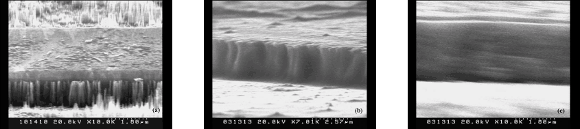
Another property of crystallographic wet etching in boiled KOH was useful for device processing and laser cavity formation. [Reference Stocker, Schubert and Redwing13] The boiled KOH stops etching GaN at {10-10} and (0001) faces and prefers etching dislocation sites. As shown in Figure 4(a), the stripped sidewall and residual dislocations on the etched surface of (0001) will limit the application to electronic or optical devices. To eliminate this limitation, boiled KOH was used to treat the PEC etched surface and the result is shown in Figure 4(b). The sidewall was smoothed and the dislocations were removed after the post-treatment by boiled KOH. By virtue of careful control of etch time and KOH concentration, a very smooth and vertical facet was achieved as shown in Figure 4(c) at {10-10} face. The striation on sidewall edge was resulted from pattern transfer during the lithography step.
Conclusions
In summary, YL-related defects induced during the PEC etching process were studied. By using PL spectroscopy, the defects were suggested to be VGa-ON. After post-treatment in a boiled KOH solution with lower concentration for a short time, the thin damaged layer was removed. With help of the crystallographic wet etching in boiled KOH solution, smooth etch surfaces and facet sidewalls can be achieved. The residual dislocations are also taken off by boiled KOH. This novel process provides a near damagefree etching for electronic and optical device application.

Figure 4. SEM of PEC etching GaN (a) PEC etching with sidewall roughness and dislocation residual at the etching surface (b)boil KOH solution post-treatment to remove residual dislocation (c) a vertical and smooth etching profile by crystallography etching with boil KOH. solution
Acknowledgements
Some samples was provided by Opto-Electronics and System Laboratories, Industrial Technology Research Institute. Financial support was provided by the and National Science Council of Republic of China (Contract No. NSC 88-2215-E-007-011).