


Introduction
Laser micromachining is a noncontact process offering selective material removal with high precision and repeatability, and a minimal heat-affected zone (HAZ.) It can also produce flexible feature size and shape using mask-imaging methods and a computer controlled multi-dimensional scanning stage etcReference Wiener-Avnear 1 . Excimer lasers with 20∼30- ns pulse duration have been demonstrated to be suitable for various materials.Reference Bauerle 2 , Reference Fogarassy, Geohegan and Stuke 3 Excimer laser machining provides the advantage of greater photon energy to break bonds, clean cutting with less thermal effects. For example, Behrmann Reference Behrmann and Duignan 4 and Wang Reference Wang, Leger and Rediker 5 fabricated diffractive optical elements (DOE) on poly(imide) micromachined by Eximer laser. HanReference Han 6 fabricated Fabry-Perot cavity chemical sensors by silicon Eximer laser micormachining.
We are interested in wide bandgap materials, particularly AlN, since it has great potential in an array of electro-optical and photonic devices. Conventional micromachining techniques, such as wet chemical, are not suitable for processing wide bandgap semiconductors. Although plasma etching is a popular method of micromachining, the possibly introduced damage makes it less suitable for precise micromachining. AlN is not etched by traditional chemical methods. Only concentrated KOH and analogous base etchants are reasonable. Furthermore, the chemical etching process is highly isotropic. Even ion beam and other plasma etching techniques are not viable solutions due to parasitic (with respect to waveguide performance) damage of the structure. With its advantages of direct writing and greater photon energy for cool ablation, we hope to utilize Excimer laser micromachining technique to fabricate photonic device structures on AlN in a one-step process. An image-based pulse KrF Excimer laser micromachining system has been developed. With an ultra-precise 4-dimensional (X, Y, Z and Rotation) scanning stage and an in-house developed software package, this system has the capability to produce feature size down to less than 1 micron scale with flexible shaped features possible.
Wave guide structures and a pixilated structure of AlN on Silicon (111) and SiC have been fabricated. The focus of this paper is to study the relation between laser ablated hole depth to the incident pulse energy for the thin film and substrate structures. Linear dependence within the thin film and substrate has been observed. This quantitative relationship provides a methodology for precise depth control, which is critical in fabrication of electronic and photonic device structures.
Experiment and Results
The experimental configuration of the Excimer laser micromachining system is shown in Fig.1. A Lambda Physik 200i Excimer laser, operating at KrF mode with emitting laser wavelength at 248-nm, is used as a laser micromachining source. The laser pulse can reach an energy as high as 600 mJ with a pulse duration of 25-ns and has a rectangular output beam of 23 mm × 8 mm. The laser beam passes through a neutralized continuously tunable attenuator and a homogenizer made of micro-lens arrays. The micro-lens arrays split the beam into different beamlets travelling along different paths and overlap them on the plane to be irradiated, which in our system is a mask. The gaussian beam profile of the laser pulse is then transformed to a near perfect flat-top shape with 0.87 flatness (see Fig. 2.). The mask is put in the homogenized plane (with a homogenized illumination area of 18 mm ×18 mm) and imaged by an objective onto the sample. The sample is placed on the top of an ultra-precision 4-dimensional scanning stage (Newport PM500, X, Y, Z and rotation; X and Y with 80 mm travel limit and 0.05 um-linear resolution; Z with 25 mm travel limit and 0.025 um linear resolution; rotation stage with 3600 travel and 0.00030 rotary resolution). A photon beam profiler is used to measure the laser beam intensity profile, a pyroelectric energy sensor is used to measure the laser pulse energy, and a fast-response Hamamatsu photodiode is used to measure the laser pulse time shape. A software package has been developed to control the laser micromachining system, including control of the Excimer laser, sample scanning stage to control micropatterning design and fabrication, and laser beam characterization.
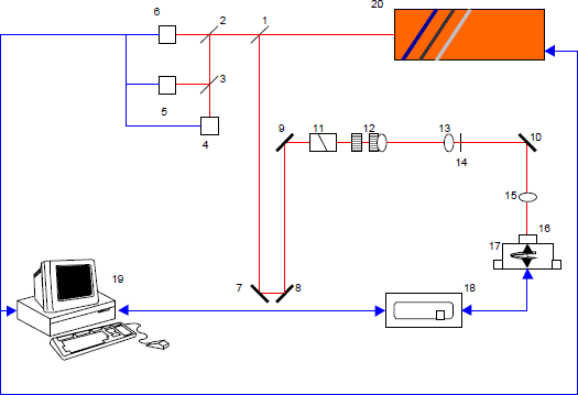
Figure 1 EXCIMER LASER MICROMACHINING SYSYTEM 1, 2, 3 Beam splitter; 4 Beam profiler; 5 Pulse shape time analyzer; 6 Energy meter; 7, 8, 9, 10 450 HR mirror; 11 Attenuator; 12 Homogenizer 13 Field lens; 14 Mask; 15 Objective; 16 Sample; 17 4-Axis precision stage; 18 Motion controller; 19 PC; 20 LPX205i Excimer Laser (KrF).
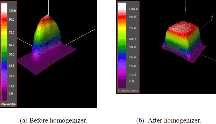
Figure 2 LASER BEAM INTENSITY PROFILES
Ablation Study
Precise control of micromachining depth is critical for the fabrication of electronic and photonic device structures. To control the depth, the relation between laser ablated feature depth and laser pulse energy must be known. We developed a routine to quantitatively explore this dependence. Utilizing a 1mm diameter pinhole as a mask, 10 × 10 arrays of holes (see Fig. 3), separated by 200 μm, are ablated in each sample (after transversing the objective, the laser beam cross section is demagnified 10X to a 100 μm spot size on the sample surface). Each of the 10 holes within a row are shot with the same number of laser pulses and the same pulse energy at a pulse repetition frequency of 25 Hz. The holes in the subsequent rows are exposed by the same single pulse energy, but the pulse number is increased. The final energy at every hole is obtained by summing the energy of the individual pulses. The sample, after micromachining, is taken for surface profile measurement using a Tencor P-1 long range scan profiler. The hole depth and the total energy of each row are averaged to minimize the influence of surface non-uniformity and laser energy fluctuation during scanning.
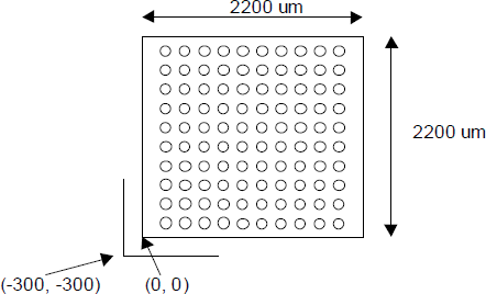
Figure 3 10×10 HOLE ARRAY
AlN thin films were deposited on Silicon (111) and r-plane sapphire substrates by plasma source molecular beam epitaxy (PSMBE).Reference Auner, Lenane, Ahmad, Naik, Kuo, Wu and Prelas 7 Crystal morphology and high quality of AlN were already reported by our group. Considering the space allowed in this paper, we refer the sample quality information of AlN to our former reports. Reference Auner, Jin, Naik and Naik 8 , Reference Thompson, Drews, Huang and Auner 9 , Reference Krupitskaya and Auner 10
Two arrays were ablated on raw Silicon (111) substrates at single pulse energy of 0.5 mJ. In the first array, the number of laser pulses were increased from 10 to 20 in one pulse increments; in the second array, the number of laser pulses were increased from 10 to 100 in increments of 10. Feature height vs. total pulse energy is shown in Fig.4. The sample surface before laser irradiation is set 0. Linear fitting results in an ablation rate of 152 angstrom/mJ.
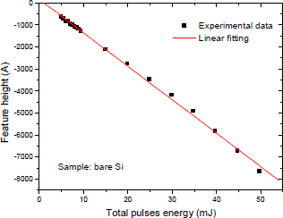
Figure 4 ABLATION RATE FOR SILICON (111)
Arrays were then micromachined in a 2400 angstrom AlN thin film on a Si (111) substrate at single pulse energy of 0.1mJ. Upon one laser pulse, the irradiated sample surface increased to a height 216.3 angstroms above the film surface, subsequent shots ablate the film at a non-linear rate until, after 10 shots, the film is ablated 259.6 angstroms lower than the surface. The mechanism for this phenomenon is unknown, and is still under investigation. It may possibly be the surface morphological change due to the crystal regrowth after low energy laser irradiation. Increasing the pulse number, we find the hole depth reaches 1500.9 angstroms after 30 pulses. At 40 pulses the bottom of the laser drilled hole is no longer flat, but irregular. We believe the AlN film has been ablated to the interface. However, increasing the pulse number to 100, edges of the hole are sharp cut and the hole bottom is flat at the depth of 3135.9 angstroms.
Feature height vs. total energy for the first AlN thin film on Si(111) is plotted in Fig.5a. The plot can be divided into three regions A, B and C, based on the different slopes. The first region describes AlN thin film ablation with an ablation rate of 690 angstrom/mJ. Region B describes ablation of the interface between AlN and Si, while region C indicates ablation of the Si substrate. In region B, we did not put in the data points since line profiles of laser ablated holes show dramatically large fluctuation of hole bottom depth values, and it has no statistical meaning, which may be taken as an indicator of the film thickness. It is the same reason for not showing data points in region B within the subsequent figures. For this sample, fluctuation occurs in the range of 2200 to 2500 angstroms, which is in agreement with the previously measured film thickness value.
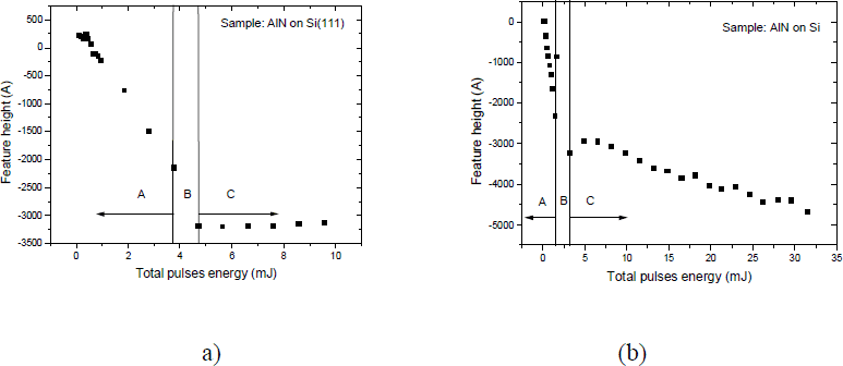
Figure 5 FEATURE HEIGHT VS. PULSE ENERGY OF AlN/Si(111)
A second AlN thin film with a thickness of 2450 angstroms on Silicon (111) was micromachined at single pulse energy of 0.164 mJ with similar incremental increases in the number of pulses. Feature height vs. total energy for the second AlN thin film on Si(111) is plotted in Fig. 5b. Similar to the first AlN on Si sample, Figure 5b shows three distinct regions. Region A shows the ablation of AlN at a rate of 1567 angstroms/mJ, region B suggests the thickness of AlN is approximately 2300 angstroms, close to the measured value. Region C shows the ablation of the Si substrate at a rate of 67 angstroms/mJ. Several steps are found with increasing number of pulses. The ablation rate of AlN for this sample is greater than that of the former sample likely due to the different AlN crystalline quality, however, further characterization needs to be done for these two samples.
AlN with thickness of 2150 angstroms on r-plane sapphire was also micromachined. The single pulse energy was set at 0.166 mJ. The ablation rate was determined from Fig. 6. At 1 pulse shot, the laser irradiated sample point ablates 194.2 angstroms; however after only 2 pulses, the line profile measures a depth of 2530.9 angstroms, showing that AlN has been completely ablated. From Fig. 5 it is estimated that 3 mJ laser pulse energy would remove this thickness of AlN. The ablation rate for saphire is found to be 656.7 angstroms/mJ, much higher than that of AlN on Si(111). Thermal effects as well as differences in crystal quality may explain the ablation rate difference of the AlN thin film on sapphire.
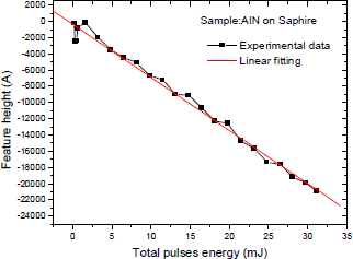
Figure 6 FEATURE HEIGHT VS. PULSE ENERGY OF AlN/Sapphire
Figure 7 shows a 3D surface profile image of laser a micromachined array on AlN/Si (111) as observed by an optical profiler from Veeco- NT2000. Please note that image is presented inverted for clarity. With the sharp cut groove structure, this laser micromachined feature may be utilized as a waveguide structure. Employing an image mask, a pixilated structured was fabricated micromachining AlN on SiC. 2000 pulses with a single pulse energy of 10mJ at the sample surface, resulted in a pixilated structure which may find applications in biosensors (see Fig.8).

Figure 7 3D OPTICAL PROFILE IMAGE OF LASER MICROMACHINED ALN/Si(111)

Figure 8 SEM IMAGE OF MICROPATTERNING ON ALN/Si(111)
Conclusion
In this paper, we have determined the ablation rates for AlN on different substrate materials, including Si (111) and r-plane sapphire. Linear dependence of the laser micromachined feature depth with the incident laser pulse energy within thin film and the substrate regions has been observed. Employing the experimentally obtained ablation rate for AlN, a waveguide structure and a pixilated structure were fabricated.
Acknowledgements
This work was supported by Smart Sensor and Integrated Devices Program at Wayne State University and National Foundation Grant 9870720. The authors gratefully acknowledge Lihua Li’s help on using Tencor P-1 scanning profiler. We also thank Dan Durison and Thomas Daley for their technical support and helpful discussions.


