Introduction
Blue light emitting diodes (LEDs) and blue laser diodes (LDs) have been developed recently using InGaN quantum wells (QWs) as the active layers and are being used in full-color display and high-density optical storage [Reference Nakamura1,Reference Nakamura and Fasol2]. GaN QWs are also of great interest for the development of new UV light emitters and for fundamental research into strong quantum confinement systems, since the huge band offsets between GaN and Al(Ga)N are favorable for increasing quantum confinement energy or reducing emission wavelength.
Large quantum confinement requires epitaxial growth of AlxGa1−xN barrier layers with high aluminum contents x, on which very thin GaN well layers have to be formed with precise control of layer thickness and surface smoothness. Although photoluminescence (PL) spectra from thin GaN QWs have previously been reported, peak wavelengths were not very much lower than the bulk value. This is because the aluminum contents x in AlxGa1−xN barrier layers were around 10-20 % and, therefore, barrier heights or band offsets were small [Reference Langer, Simon, Ortiz, Pelekanos, Barski, Andre and Godlewski3-Reference Grandjean and Massies13]. Recently, Hirayama and Aoyagi have reduced the PL wavelength down to 280 nm by using Al0.11Ga0.89N for QW layers [Reference Hirayama and Aoyagi14,Reference Hirayama and Aoyagi15]. However, to realize stronger quantum confinement and shorter emission wavelengths, further development of the epitaxial growth of nitride semiconductors is very important.
In this work, we measured PL spectra at room temperature for GaN QWs with Al0.8Ga0.2N barriers, which were grown by atmospheric-pressure metal organic chemical vapor deposition (MOCVD). The thickness of the GaN QW layers was systematically varied from one monolayer (ML) to four MLs. We have achieved PL emission at a wavelength as short as 247 nm (5.03 eV) in 1ML QWs. The effective confinement energy, or difference between this recombination energy and the band gap of bulk GaN, is as large as 1.63 eV. Such strong confinement was achieved by reducing the well thickness down to 1 ML and increasing the aluminum content x in the AlxGa1−xN barrier layers up to 0.8.
Sample Preparation
We grew four samples of GaN multiple QWs (MQWs) containing well layers of different thicknesses, viz., 1, 2, 3, and 4 MLs, in an atmospheric-pressure two-flow MOCVD system with a horizontal quartz reactor. After growing a 30-nm-thick GaN nucleation layer at 480 °C on a (0001)-oriented sapphire substrate, a 1.5-μm-thick GaN buffer layer was deposited at 1071 °C. During the growth of the GaN buffer layer, the flow rate of TMG was 88 μmol/min with carrier gases of H2 at 4 l/min and N2 at 12 l/min. NH3 was used as the group V source with a flow rate of 4 l/min, which corresponds to a V/III ratio of about 2000. Then, the substrate was heated up to 1092 °C to grow MQW layers. The thickness of Al0.8Ga0.2N barrier layers was 3 nm, while the thicknesses of GaN well layers were from 1 ML to 4 MLs. The layer thickness and aluminum content in the AlGaN barrier were carefully determined by x-ray diffraction (XRD) rocking curves. The flow rate of TMG was 16 μmol/min for the GaN well layers, while those of TMG and TMA were 2 μmol /min and 8 μmol /min, respectively, for the Al0.8Ga0.2N barrier layers. For both layers, the flow rates of NH3, H2, and N2 were maintained at 4 l/min, 4 l/min, and 28 l/min, respectively. The growth rates of the GaN and Al0.34Ga0.66N layers were 141 nm/hr and 87 nm/hr, respectively.
Photoluminescence Properties
PL spectra were measured at room temperature for the four GaN MQW samples. The excitation source was an excimer laser (ArF) with a peak wavelength of 193 nm and a repetition rate of 100 Hz. This laser excites both GaN well layers and Al0.8Ga0.2N barrier layers. The PL from the QWs was dispersed by a 30 cm monochromator and detected by a cooled charge-coupled device (CCD) camera.
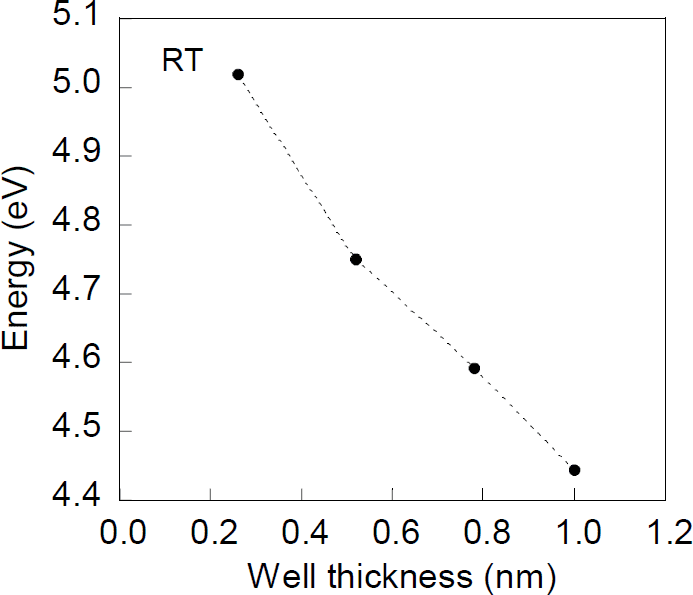
Figure 1 shows PL spectra for 1, 2, and 3 ML GaN QWs. PL peaks are clearly observed in 2 ML and 3 ML QWs, with peak wavelengths of 260 nm and 270 nm, respectively. In the 1 ML QW sample, the wavelength of the main PL peak is as low as 247 nm (5.03 eV). The effective confinement energy, or difference between the recombination energy and the band gap of bulk GaN, is as large as 1.63 eV in the 1 ML QWs. The wavelengths of the PL peaks are plotted in Fig. 2 as a function of well thickness together with the value for the 4 ML QW sample. The significant blue shifts are due to the quantum confinement effect. PL from barrier layers could not be seen because their thickness is very thin (3nm).

Figure 1 Photoluminescence spectra for GaN quantum wells, whose thicknesses are from one monolayer to three monolayers, measured at room temperature.

Figure 2 Peak wavelength in photoluminescence spectra is plotted as a function of the thickness of GaN well layers.
The linewidth of the main peak is 240 meV for 1 ML QWs. This value is in fairly good agreement with the theoretical value of energy broadening induced by monolayer fluctuations of well thickness. The linewidths of the main peaks are 230 meV and 220 meV for 2 ML and 3 ML QWs, respectively. With decreasing well thickness, the linewidth becomes just slightly smaller.
Another PL peak at 269 nm is also observed in the 1 ML QW sample. This wavelength (269 nm) coincides with the main peak of the 3 ML QWs, showing that this emission comes from localized potential minima at which the effective well thickness is 3 ML. The linewidth of the peak at 269 nm is broader than that of the main peak at 247 nm. This should be attributed to the overlapping of two peaks coming from 2 ML and 3 ML QWs, resulting in the broad peak.
PL intensities decrease monotonically as the well thickness is reduced. With reducing the thickness of GaN well layers, wave functions penetrate more into the AlGaN barrier layers. Therefore, PL efficiencies become very sensitive to the quality of the interfaces, leading to degradation of PL efficiencies.
Conclusions
We grew a series of high-quality GaN MQWs with Al0.8Ga0.2N barriers by atmospheric-pressure MOCVD and measured PL spectra at room temperature. The peak wavelength of 1 ML GaN QWs reached a value as short as 247 nm (5.03 eV). This result means that the effective quantum confinement energy is 1.63 eV. The spectral linewidth was 240 meV, which is in fairly good agreement with the theoretical value of energy broadening induced by monolayer fluctuation. Although PL efficiencies have to be improved, light emission at such short wavelengths from thin GaN QWs should be very useful for optoelectronic devices operating at UV wavelengths.
Acknowledgements
The authors thank M. Nishioka and S. Ishida of University of Tokyo for technical support with the MOCVD system. This work is partly supported by JSPS (Project No. JSPS-RFTF96P00201), a Grant-in-Aid for Scientific Research from the Ministry of Education, Science, Sports, and Culture, and University-Industry Joint Project on Quantum Electronics.