


Introduction
Group-III nitrides (AlN, GaN, InN, and their alloys) have attracted great interest recently for their enormous potential for optoelectronic device applications operating in the spectral range from green to ultraviolet. The lack of bulk crystals for substrates is a major limitation for fully implementing such devices; the epitaxial growth of nitrides is currently limited to foreign substrates, mainly sapphire and SiC Reference Monemar[1]. Bulk crystal AlN will provide a superior substrate for group-III nitride epitaxial layers as it is closely lattice and thermal expansion matched to GaN. It has many favorable properties such as high thermal conductivity, low thermal expansion coefficient, high electrical resistivity, good dielectric properties, and excellent oxidation resistance.
Most studies of AlN bulk crystal growth have employed the sublimation method, as AlN's high melting temperature (>2700°C) makes it impossible to grow from melt Reference Krukowska-Fulde and Niemyski[2] Reference Ishii, Sato and Iwata[3] Reference Slack and McNelly[4] Reference Tanaka, Nakahata, Sogabe, Nakata and Tobioka[5]. A bulk AlN crystal of 470 mm3 was produced by self-seeding in the sharp tip of a sealed tungsten crucible by Slack and McNelly Reference Slack and McNelly[4] during mid-70s. The group of Schowalter and Slack et al. Reference Schowalter, Rojo, Yakolev, Shusterman, Dovidenko, Wang, Bhat and Slack[6] Reference Schowalter, Shusterman, Wang, Bhat, Arunmozhi and Slack[7] continues to improve on this technique and have reported producing crystals up to 19mm in diameter. 6H-SiC substrates offer an alternative method of seeding even larger AlN crystals by sublimation due to the easy nucleation and crystal orientation control. Balkas et al. Reference Balkas, Sitar, Zheleva, Bergman, Nemanich and Davis[8] grew seeded single crystalline platelets of AlN less than 1mm thick on a 10×10 mm2 6H-SiC in a resistively heated graphite furnace. Growth rates up to 0.5mm/hr were achieved at 2150~2250°C and a nitrogen pressure of 500 torr. However, the AlN films contained individual hexagonal crystals (≈; 2 × 2 mm2), and Si, C and O were incorporated into the AlN, from the SiC coated graphite crucible. Sarney et al. Reference Sarney, Salamanca-Riba, Hossain, Zhou, Jayatirtha, Kang, Vispute, Spencer and Jones[9] also grew AlN on 6H-SiC between 2150°C and 2200°C, with nitrogen pressures of 400~410 torr. The growth rate was varied between 10 and 50 μm/h. But the same problems still exist, i.e. the AlN cracks and contains high screw dislocation density due to the stress caused by the thermal expansion coefficients mismatch. Karpov's group Reference Karpov, Zimina, Makarov, Mokhov, Roenkov, Ramm and Vodakov[10] Reference Segal, Karpov, Makarov, Mokhov, Roenkov, Ramm and Vodakov[11] grew AlN layers 60 to 80 μm thick of 10 × 10 mm2 size on 6H-SiC as the seed at 1700~2300°C under both atmospheric pressure and in vacuum (10−4 torr). No characterization of these crystals was presented. In short, AlN deposited on SiC generally has high dislocation densities and multiple small size grains. Thus more research work is necessary to improve growth technique.
A thorough investigation of the growth mode and defects for AlN sublimated on the SiC substrates prepared by different techniques is critical for preparing high quality bulk crystals free of cracks and screw dislocations. In this paper, we focus on the crystal growth mode and defects in AlN grown on different (0001) 6H-SiC substrates. The effects of the substrate preparation on the growth mode and types of defects presented are examined in detail.
1. Experimental
1.1 Sublimation Apparatus
The experimental setup for AlN sublimation, which is shown in Figure 1, was described in detail in the previous work Reference Liu and Edgar[12]. Briefly, the Al and N2 vapor created by the dissociation of the hot polycrystalline AlN source (Ts ~ 1900°C) are transported to a seed held at a lower temperature (Tc ~ 1800°C) in a 30 mm diameter tungsten crucible. Then adsorption/desorption takes place at the seed crystal surface leading to growth. The sublimation is carried out in ultra-high purity N2. The temperature and temperature gradient are maintained by a resistively heated tungsten element and the pressure is automatically maintained at a constant value (400 torr). Sintered AlN with approximate 0.6 wt% oxygen as the main impurity (as analyzed by a standard inert gas fusion method) was the source material. Growth runs varying from 10 minutes to 40 hours were employed.
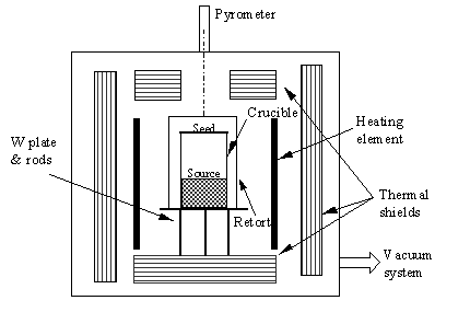
Figure 1. Schematic view of AlN sublimation growth system
The in-situ growth temperature was measured by the same optical pyrometer focused on the top lid of the retort and controlled by the output power.
1.2 Substrate Preparations
6H-SiC single crystals of various orientations and surface preparation were used, to determine their influence on the AlN growth mode. There was almost no growth on C-face substrates, thus only Si-face SiC substrates were used, including on-axis as-received (0001) SiC, on-axis (0001) SiC with an AlN buffer layer deposited by MOCVD, on-axis (0001) SiC with a 3C-SiC epitaxial layer, off-axis as-received (0001) SiC, off-axis (0001) SiC with an AlN buffer layer deposited by MOCVD, and off-axis (0001) SiC with a 6H-SiC epitaxial layer.
The AlN buffer layer was grown in a vertical MOCVD induction heated reactor. Trimethylaluminum (TMA) and ammonia (NH3) were utilized as Al and N sources, and Pd-cell purified H2 was the carrier gas. The epilayer was deposited at 1000°C and 80 torr under the H2, NH3 and TMA flow rates of 6 slm, 3 slm and 60 sccm respectively. An approximate 1.5 μm thick AlN film was obtained for 2 hours run.
The SiC epitaxial layer was grown at horizontal-type atmospheric pressure CVD. After etching in a mixture of hydrogen and HCl at 1400°C, SiC epitaxial layers were deposited at 1400~1500°C with a silane (SiH4) flow rate 0.5 sccm, ethylene (C2H4) flow rate 0.7 sccm, and H2 flow rate 8 slm. An approximate 1.0 μm thick 6H-SiC film on off-axis 6H-SiC or 3C-SiC film on on-axis 6H-SiC was deposited in 30 minutes.
1.3 Morphology Characterization Techniques
Macrostuctrual features in the AlN crystals were characterized by Nomarski differential interference contrast microscopy. The surface morphology was examined by scanning electron microscopy (SEM) up to 2000×. Steps and terraces in the surface morphology of some samples were examined by atomic force microscopy (AFM) in contact mode.
2. Results and Discussion
2.1 As-received On-axis and Off-axis 6H-SiC
On on-axis and off-axis as-received 6H-SiC substrates, the AlN deposited in an island growth mode promoted by screw dislocations. The AlN grains were 1mm to 2mm in size after several ten hours of growth. Hexagonal sub-grains and grain boundaries are clearly evident in the optical micrograph for AlN deposited on such substrates (Figure 2).

Figure 2. Optical micrograph of AlN crystal surface grown on on-axis, as-received (0001) 6H-SiC substrate at 1780 °C and 400 torr for 40 hours with the magnification100× (The real width of the crystal in above image is 1.0 mm).
Screw dislocations provide the steps for the growth of crystal. The terrace width between steps is about 0.3 μm, as determined by SEM image shown in Figure 3, and the step height was about 20 nm, as determined by AFM. This shows that the diffusion length of Al or N atoms on the surface is too small to enhance a 2-dimensional nucleation and growth. The large thermal stress between substrates and deposited AlN results in high screw dislocation density. Figure 4 (a) and (b) show the surface of AlN nucleated on the on-axis and off-axis as-received SiC substrates. The randomly nucleated hexagonal hillocks (black spots) on the SiC surface gradually merged together as AlN growth progressed. This merging produced the grain boundaries seen in Figure 2.
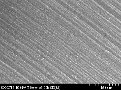
Figure 3. SEM of AlN crystal surface grown on on-axis as-received (0001) 6H-SiC substrate at 1780 °C and 400 torr for40 hours with the magnification 2000×.

Figure 4. Optical micrograph of AlN crystal grown on as-received (0001) 6H-SiC substrate at 1780°C, 400 torr for 2 hours with magnification 100×: (a) on-axis (b) off-axis. (The real width of crystal in above image is 1.0 mm).
The large stress introduced by the cooling from sublimation temperature to the room temperature, cracked the AlN into small pieces several mm in size. Occasionally the SiC substrate peeled off from thicker bulk AlN crystal, as shown in Figure 5. The cracks in the AlN crystal did not coincide with the boundaries of sub-grains. At higher temperature (>1840°C), the AlN surface became more rough, and several holes appeared on surface due to substrate decomposition. Figure 6 shows a SEM image of an AlN film grown on on-axis 6H-SiC substrate at 1890°C and 400 torr for 20 hours. Cracks, holes and even grains are apparent in the AlN film.
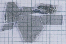
Figure 5. AlN bulk crystals peeled off from the on-axis, as-received (0001) 6H-SiC substrate on which they were deposited. The crystals were grown at 1780°C and 400 torr for 40 hours (grid size is 1 mm)
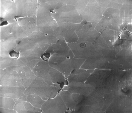
Figure 6. SEM of AlN grown on on-axis as-received (0001) 6H-SiC substrate at 1890°C and 400 torr for 20 hours with magnification 20× (real width of above crystal is 1.0 cm).
2.2 On-axis and Off-axis 6H-SiC with AlN buffer layer
An AlN buffer layer is commonly used in the GaN epitaxy on SiC substrate, to promote the wetting of substrate surface. In the sublimation growth of AlN, an AlN buffer layer significantly changed the growth mode and decreased the screw dislocations. Figure 7 (a) and (b) show the surface morphology of AlN grown on the on-axis and off-axis 6H-SiC at 1780°C, 400 torr for 10 hours with AlN buffer layer deposited at 1100°C 80 torr for 3 hours. The rings are interference patterns caused by stress in the films, and the black lines are cracks. The surface of the AlN film on the on-axis substrate is smoother than on the off-axis SiC, where parallel steps are distributed regularly on the growth surface.

Figure 7. Optical micrograph of AlN crystal surface grown at 1780°C and 400 torr on (0001) 6H-SiC substrate for 10 hours with an AlN epitaxial layer. The magnification is 100×: (a) on-axis, (b) 8o off-axis. (The real width of crystal in above image is about 1.0 mm).
As expected, the AlN epilayer (about 1.5 μm) changed the growth mode of AlN sublimated on the SiC substrate. Figure 8 (a) and (b) show the surface of AlN nucleated on the on-axis and off-axis SiC substrates. In these thin films (about 20 μm thick), the cracks were regularly located in the (10
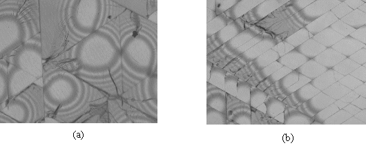
Figure 8. Optical micrograph of AlN crystal grown at 1780°C, 400 torr for 2 hours on (0001) 6H-SiC substrate with an AlN epitaxial layer. The magnification is 1003: (a) on-axis (b) 8o off-axis. (The real width of crystal in above image is about 1.0 mm).
Although AlN crystals grown on the SiC with an AlN buffer layer had much lower dislocations, cracks were still inevitable in these experimental runs with AlN layers less than about 400 μm thick, as shown in Figure 9. The growth mode may change with the increase of thickness, which is encountered in III-nitride epitaxy especially for quantum dots fabrication Reference Davis, Tanaka and Scott Kern[13] Reference Daudin, Feuillet, Mula, Mariette, Rouviere, Pelekanos, Fishman, Adelmann and Simon[14]. Efforts are still taken to grow pure thicker and larger AlN crystals in 2-D growth mode.
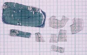
Figure 9. AlN bulk crystal grown on on-axis AlN-buffered (0001) 6H-SiC substrate at 1780°C and 400 torr for 40 hours (grid size is 1 mm, left big pieces with darker color are peeled SiC substrate, other smaller ones with light color are peeled AlN).
2.3 On-axis and Off-axis 6H-SiC with SiC epitaxial layer
Wilson et al. Reference Wilson, Dickens, Griffin and Spencer[15] found that deposition of AlN epilayers on off-axis 6H-SiC and 4H-SiC with an initial SiC epilayer displayed high quality step flow growth. The APCVD epitaxial growth of off-axis SiC resulted in uniform steps with height of 1.5nm, i.e. 6 bilayers and narrow step width of about 70 nm compared with about average 200nm of singular substrate in our experiments. As-received off-axis 6H-SiC and on-axis 6H-SiC have various step heights of different number of layers as well as non-uniform step width according to our AFM examination. Step bunching occurs when an additional epitaxial SiC layer was deposited on the initial off-axis substrate. The step bunching brings about 6-bilayer step height and uniform step width due to the different growth rate of different stacking layer.
Figure 10 shows the morphology of AlN nucleation and growth on the on-axis and off-axis SiC substrates with about 1 μm SiC epitaxial layers. Hexagonal hillocks were still observed on the on-axis substrates with 3C-SiC epilayer while step flow growth is clearly displayed on the off-axis substrates with 6H-SiC epilayer.
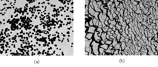
Figure 10. Optical micrograph of AlN crystal grown at 1870°C, 400 torr for 2 hours on on-axis (0001) 6H-SiC substrate with about 1 μm SiC epitaxial layer. The magnification is 1003: (a) on-axis; (b) 8o off-axis. (The real width of film in above image is about 1.0mm).
Unfortunately, we could not keep step flow growth mode at initial nucleation stage on off-axis substrates for long time (>10 hours). The step bunching happened during the step flow growth. The SEM observation shown in Figure 11 indicates that hexagonal nucleation was taking place in the wide terrace or at the edges of the steps, which is attributed to the low mobility of AlN.
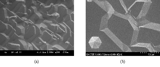
Figure 11. SEM of AlN grown on 8o off-axis (0001) 6H-SiC substrate with about 1 μm SiC epitaxial layer at 1870°C, 400 torr for 2 hours with magnification 2000: (a) 200times (b) 2000×.
3. Summary and Conclusion
The effects of substrate misorientation and buffer layers (both SiC and AlN) on the morphology of AlN deposited on 6H-SiC were analyzed. On-axis and off-axis 6H-SiC wafers without any treatment, or with AlN buffer layers, or with SiC epilayers, have been utilized as the substrates for AlN sublimation growth.
The AlN sublimated on the on-axis and off-axis 6H-SiC substrate without any treatment proceeded by island growth, producing a high density of screw dislocations. This produced individual AlN grains and rough surface morphologies. These problems were largely eliminated by first depositing an AlN layer on the 6H-SiC by MOCVD before starting sublimation growth. 2-dimensional growth was achieved on the 6H-SiC with AlN-buffered layers and no screw dislocations were observed. At last, growth on off-axis SiC with 6H-SiC epilayers had the step flow growth mode, but with the increasing of step width, hexagonal nucleation hillocks deposited on terraces.
Step width played an important role on the growth mode. Different growth modes were attributed to the low mobility of AlN adatoms on crystal surface. In our growth condition, the surface mobility may be too low to annihilate the domain boundary at large step width such as several hundred nm. Increasing temperature is a way to solve this problem. But the temperature is two-edged sword, it can not only increase the surface mobility and hence the grain size, but also enhance the decomposition of SiC and hence contaminate the AlN crystal.
ACKNOWLEDGMENTS
The financial support of the Office of Naval Research through grants number N00014-97-1-0332 and N00014-99-1-0104 is gratefully appreciated.


