Introduction
GaN-based semiconductor lasers are promising for light sources of high-density optical data storage systems, because of their short wavelength of around 400nm. However, we have worked with much effort for a long time in order to obtain a high quality crystal, because of the lack of substrates lattice-matched to this material system. In 1986, on the growth method using a LT-buffer layer[Reference Amano, Sawaki, Akasaki and Toyoda1] on sapphire substrate, which has a large lattice-mismatch of about 16%, GaN film with an excellent flatness and crystallinity was successfully obtained. Further, p-type low resistance crystal was realized by Mg-doping and electron-beam irradiation [Reference Amano, Kito, Hiramatsu and Akasaki2], or anneal process [Reference Nakamura, Iwata, Senoh and Mukai3]. After such progress, high brightness blue and green light emitting diodes (LEDs) have been realized [Reference Akasaki and Amano4],[Reference Nakamura, Mukai and Senoh5]. More recently, several groups have achieved continuous-wave (CW) operation of violet-blue laser diodes(LD)[Reference Nakamura, Senoh, Nagahama, Iwasa, Yamada, Matsushita, Sugimoto and Kiyoku6]-[Reference Kuramoto, Sasaoka, Hisanaga, Kimura, Yamaguchi, Sunakawa, Kuroda, Nido, Usui and Mizuta9]. It is thought that the GaN-based LD for the practical use will be commercially available in the near future.
However, the further improvements concerning with a crystalline quality and device performance are required against the practical use. In general, high quality GaN layer is grown on LT-buffer layer / sapphire substrate. When the AlGaN layers, commonly used as cladding layers in LDs, are grown on the GaN layer, the crack is often observed in the surface. This is thought to be due to the difference of lattice constants between GaN and AlGaN. Therefore, the thickness and AlN molar fraction of AlGaN layer, which are considerably important for the device performance, are greatly limited in order to avoid the crack generation.
The beam profiles of GaN-based diode laser in the direction perpendicular to the junction (vertical mode) are tend to be composed of multiple spots, which can be seen in the far field pattern [Reference Hofsteller, Bour, Thornton and Johnson10],[Reference Nakamura11]. A poor optical confinement causes optical leakage from a waveguide layer to the underlying layer, such as an underlying n-GaN base layer. In order to suppress this optical leakage, the thickness of an AlGaN cladding layer should be much thicker than that usually embedded in a conventional structure. However it is quite difficult to grow crack-free thick AlGaN directly on GaN as mentioned above. Thus, the suppression of the crack in AlGaN is important subject for the improvement of device performance.
In this report, we demonstrate a crack-free Al0.07Ga0.93N layer with the thickness of more than 1μm using underlying AlGaN layer grown directly on LT-buffer layer. We confirmed that the crystalline quality of AlGaN just on the LT-buffer layer is comparable as that of GaN. We also achieved a single-robe far field pattern in the LD with the thick and crack-free n-AlGaN layer as a cladding layer.
Crystal Growth
In a conventional laser structure, whose schematic diagram is shown in Fig. 1(a), a n-GaN layer grown just on the LT-buffer layer is used as a base layer for laser structure, as well as a n-contact layer. However, this layer might cause the crack in n-AlGaN cladding layer grown on the layer, because of the tensile strain from the difference of lattice constants between GaN and AlGaN. We applied a new approach to overcome the problem that n-AlGaN is used as the base layer shown in Fig. 1(b). We investigated a crystalline quality of n-Al0.05Ga0.95N layer directly grown on the LT-buffer layer / sapphire substrate, using X-ray diffraction measurement and transmission electron microscopy (TEM). The FWHM of X-ray rocking curve was about 400 arcsec, and dislocation density from TEM image was 4×109cm−2, which values are comparable to those of GaN grown on LT-buffer layer. From these results, the n-Al0.03Ga0.97N layer directly grown on the LT-buffer layer has a capability for the base layer of GaN-based laser diodes.

Figure 1: Schematic of laser structure with AlGaN/LT-buffer/sapphire.
Laser structure was grown on c-face sapphire substrates by low-pressure metalorganic vapor phase epitaxy. In the new structure shown in Fig. 1 (b), instead of underlying n-GaN layer, a 4 μm thick n-Al0.05Ga0.95N layer was directly grown on LT-buffer layer. After the growth of the underlying n-Al0.05Ga0.95N layer, the other layers of laser structure were grown, which are 1μm n- Al0.07Ga0.93N cladding layer, 0.1μm n-GaN guiding layer, 3 nm Ga0.9In0.1N / 10 nm Si-doped Ga0.98In0.02N 3QWs active layer with 15nm Al0.15Ga0.85N electron blocking layer, 0.1μm p-GaN guiding layer, 0.5μm p-Al0.07Ga0.93N layer, and 0.1μm p-GaN contact layer.
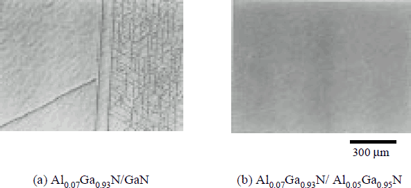
The surface morphologies of the conventional and the new laser structures are shown in Fig.2. The conventional laser structure has many cracks due to the lattice mismatch between GaN and Al0.07Ga0.93N, while the new structure does not have any crack. From the X-ray diffraction measurement, we have obtained the tensile strain in n-Al0.07Ga0.93N layer of new structure is about 0.06%, which value is almost the halt in the case of conventional structure. This lower tensile strain could contribute to few cracks in the wafer irrespective of thicker n-Al0.07Ga0.93N layers.

Figure 2: Surface morphologies of the laser structures
Device Performance
Using this laser wafer, we fabricated the 2-μm-wide ridge waveguide devices with 500-μm-long cavity. The laser facets were formed by cleaving along (1-100) plane of sapphire. High reflection coating was performed on the facets (front:80%, rear: 90%).
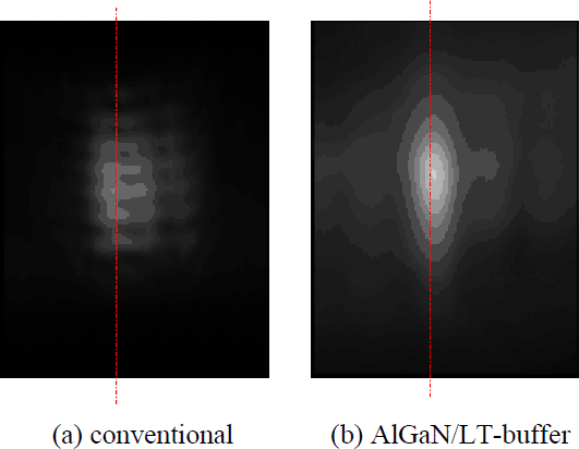
Figure 3 shows L-I characteristics of the new type laser. The measurements were pursued at room temperature under pulsed condition with a duty ration of 0.05 %. The threshold current of this device is as low as 65mA, which corresponds to threshold current density of 6.5 kA/cm2. This value is equal to or better than that of conventional one in our experiments, indicating that the material quality of layers on underlying AlGaN layer / LT-buffer / sapphire is high enough in terms of device performances. The vertical profiles of far field pattern for the conventional and the new type lasers are shown in Fig. 4. The new type laser clearly shows single peak in far field pattern, while the conventional one shows multi peak in far field pattern as other groups already reported.[Reference Hofsteller, Bour, Thornton and Johnson10],[Reference Nakamura11] These results indicate that the thick AlGaN cladding layer can successfully suppress the optical leakage from the waveguide region to the other regions. We also plotted the theoretical profiles of far field patterns calculated. The calculated results are good agreement with the experimental results.

Figure 3: L-I Characteristic under RT Pulsed Condition

Figure 4: Far field pattern of LDs
Conclusion
In summary, we have realized thick layer of AlGaN free from cracks, using AlGaN / LT-buffer layer structure. Applying the structure to laser diode, we have demonstrated a low threshold current operation and a single spot near field and far field patterns in the direction perpendicular to the junction. A 1μm Al0.07Ga0.93N cladding layer attributes to suppress the optical leakage and results in a improvement of optical confinement. This structure should be the key technology for practical use of high-performance GaN-based laser diode.
Acknowledgements
This work was partly supported by the JSPS Research for the Future Program in the Area of Atomic Scale Surface and Interface Dynamics under the project of “Dynamic Process and Control of the Buffer Layer at the Interface in a Highly-Mismatched System” and Ministry of Education, Science, Sports and Culture of Japan (High-Tech Research Center Project and contract nos. 11450131).