


Paradigm shift from processing-centric to memory-centric computing
When A. Turing suggested his “general Turing machine” in his seminal paper in 1936,Reference Turing1 he assumed infinite memory. This has never been practically realized in the history of computer development, although the modern computer is a Turing machine. Several factors must be emphasized as reasons for this. One is the difficulty in making infinitely high-density memory (even today). Another is the emergence of the complementary metal oxide semiconductor field-effect transistor (CMOSFET) in the 1960s.
CMOSFET or CMOS technology provided computer engineers with a convenient pathway to implement Boolean logic operations, leading to the development of processing-centric computers, established by J. von Neumann.Reference Bresniker, Singhal and Williams2 To understand the meaning of processing-centric computing, let us consider the following example: when a modern computer is asked to calculate, for example, the sum of numbers 2 and 3, the machine has to convert the decimal numbers to binary numbers, add them, and reconvert the binary output back to a decimal number. These processes take approximately 270 logic steps, and only approximately 30 steps are taken by the actual adding operation (a full adder). Therefore, modern computers are considered inefficient in this aspect. When a human is asked the same question, the sum is most likely recalled from the memory of the brain instead of being calculated with numbers. Can a computer do the same? Such a question was an inadequate one in the past, but is now significant. One of the reasons why so many logic steps are necessary in the previously mentioned calculation is that inefficient memory function of the processor requires that local data be copied many times in different parts of a circuit, particularly its memory, which currently consumes the largest amount of energy for the computing process.Reference Jeong, Kim, Kim, Choi and Hwang3
There are several reasons why the recall process is not available in modern computers. First, it requires an enormous amount of memory (one can imagine the number of combinations available even for such a simple mathematical sum of any two numbers—infinite). However, computers can select and memorize frequently used arithmetic operations and use their set as a lookup table. Even for such a case, there are still several problems. Data must be easily accessible, preferably in an extremely parallel manner to increase the data transfer rate, and stored in a nonvolatile memory. The current memories, dynamic random-access memory (DRAM), which is used as the working memory, and NAND flash or hard disk drives [HDDs] used as storage memory, cannot offer these functionalities.
New memories are thus necessary to keep up with the shift from processing-centric to memory- (or data-) centric computation in computer engineering or more broadly in the field of information technology (IT). Such a shift is confirmed by two changes in the field of IT. First, there has been an increase in the memory portion of the semiconductor market. Figure 1 shows the evolution of segments in the semiconductor market during the past 30 years. The memory market share has significantly increased from approximately 15% in the 1990s to approximately 22% in recent years. Power scaling according to Dennard’s Law (as transistors become smaller, their power density stays constant, such that the power use remains in proportion with the area) was stopped in 2005, and the clock speed of a processor has stayed in the range of 3–4 GHz for a decade. Development of modern processors more or less relies on parallelization (multicore technology), whereas the increase in memory integration density is still ongoing with the recent upsurge of vertical integration technology in NAND flash. There has also been an evolution of deep learning as a driver for artificial intelligence (AI). Deep learning is basically a store in memory-and-compare method, so the incorporation of huge memories and their rapid accessibility is of essential importance compared with the conventional von Neumann-type computing architecture.Reference Graves, Wayne, Reynolds, Harley, Danihelka, Grabska-Barwińska, Gómez Colmenarejo, Grefenstette, Ramalho, Agapiou, Puigdomènech Badia, Hermann, Zwols, Ostrovski, Cain, King, Summerfield, Blunsom, Kavukcuoglu and Hassabis4 All of these megatrends demand memories that are more efficient and denser than current memories.
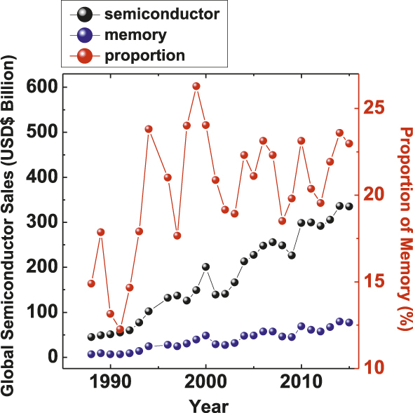
Figure 1. The trend of rapidly increasing memory proportion since the early 1990s, during the past 30 years of the semiconductor market share.
New memory concepts based on material innovation
When the international technology roadmap for semiconductors is examined, one can easily find that there are two global categories of memory—current and emerging.5 Current memory essentially refers to DRAM and NAND, because the market sizes of other memories, such as static random-access memory (SRAM) and NOR flash, are shrinking. Emerging memories can be classified into two categories—prototypical and newly emerging. The former encompass ferroelectric random-access memory (FeRAM), spin transfer torque magnetic random-access memory (STT-MRAM), and phase-change random-access memory, whereas the latter refer to a new class of FeRAMs based on newly emerging ferroelectric thin films (doped-HfO2 or (Hf, Zr)O2), redox-based resistance switching random-access memory (ReRAM), and several other newly emerging concepts, some of which will be dealt with in this issue of MRS Bulletin. For both types of memories (i.e., current and emerging), materials innovation is at the heart of their past, present, and future developments, which is more obvious for the emerging memories. We recently reviewed these material innovations.Reference Hwang6
The aim of this issue of MRS Bulletin is to review recent progress in these critical fields. The articles in this issue cover six of the most compelling topics in the field. Two charge-based memories are reviewed: higher-k dielectric films for DRAM capacitors, and HfO2-based FeRAMs and ferroelectric field-effect transistors (FeFETs). DRAM is a device that reveals the limits of scaling according to Moore’s Law. There will be an eventual halt to further scaling in DRAM, but it can be delayed by material and process innovations, particularly by the materials related to charge storage.
Kim and PopoviciReference Kim and Popovici7 cover recent progress in DRAM material and manufacturing technologies, and also discuss the future of this long-standing main memory.
The recent discovery of ferroelectricity in (doped) HfO2(-ZrO2) system has renewed interest in FeRAMs and FeFETs due to their compatibility with scaled-memory devices.Reference Park, Kim, Kim, Moon, Kim, Müller, Kersch, Schroeder, Mikolajick and Hwang8 The compatibility comes mainly from the low thickness (<<10 nm) and mature thin-film processing technique (atomic layer deposition), which has not been true for conventional perovskite-based ferroelectric materials. Nonetheless, the potential origin of such ferroelectricity in this material system, which has been used for the high-k gate dielectric of high-performance MOSFETs and capacitor dielectric in DRAM, is not clearly understood. Mikolajick et al.Reference Mikolajick, Slesazeck, Park and Schroeder9 discuss the unveiled origins of such unexpected ferroelectricity and summarize the rapid developments of such materials for memory applications.
Since charge-based memories face a fundamental limitation of scaling by the discreteness of electrons and quantum mechanical tunneling near the design rule of 5 nm, the importance of resistance-based memory has increased. Accordingly, three topics are covered for this field—topological phase-change memory, novel spin-based magnetic memory, and ReRAM without ion migration. Phase-change memory based on chalcogenides, such as Ge2Sb2Te5, has been investigated for decades, but its high power consumption and related reliability issues have hindered its widespread use as a versatile memory. TominagaReference Tominaga10 discusses the new concept of interfacial phase-change memory, wherein although the conventional macroscopic phase transition between the amorphous and crystalline phases is suppressed, fluent resistance switching is still observed from the layered GeTe-Sb2Te3 system.Reference Simpson, Fons, Kolobov, Fukaya, Krbal, Yagi and Tominaga11 This concept has been recently interpreted as a specific operation of topological phase transition, which is now boosting new research interest, especially in two-dimensional materials. Tominaga reinterpreted this intriguing aspect with more material science-friendly terms (energy-band diagram), which will contribute to the understanding of their topological behavior.
STT-MRAM is a spintronics memory relying on the tunnel magnetoresistance of magnetic tunnel junctions and the spin transfer torque phenomenon. This memory is receiving increasing interest from the microelectronics community and industry and is about to enter volume production at major microelectronic foundries. Companies intend to use STT-MRAM as a substitute for embedded flash memories and moderately fast SRAM.Reference Chi, Li, Cheng, Lu, Kang and Xie12 For high-density memories, efforts are still needed on the etching of these materials at narrow pitch and on novel material integration. Yuasa et al.Reference Yuasa, Hono, Hu and Worledge13 review the materials research and development for STT-MRAM that have allowed this technology to reach the market.
ReRAM has been highlighted as a feasible high-density memory with the potential to replace NAND flash, thanks to its repeated formation and rupture of atomic-scale conducting paths that modulate the electrical resistance. However, such resistance modulation usually involves the migration of ions, which almost inevitably induces relatively low device reliability and yield. Resistance switching does not necessarily require ionic motion of the switching media, but could be induced by an electronic origin. It was reported that electron trapping and detrapping could result in useful electrical conductivity modulation in a simple metal/insulator/metal configuration, and further studies have revealed additional merits of such a mechanism.Reference Chen, Kim, Wang, Tung and Chen14 Lu et al.Reference Lu, Yoon, Dong and Chen15 cover the basics of this performance and discuss their ReRAM device application. Their recent findings on the negative-U energy-related trapping in thin amorphous films are discussed and will broaden the understanding as well as application of these intriguing materials. These are all solid-state and nonvolatile devices, except for DRAM, which may support the processor in different scales from exascale computing in a supercomputer to smartphones.
Nonetheless, the importance of disk-type storage devices has not degraded as a requirement for data repositories and as cloud computing rapidly increases. In this regard, HDD technology will continue improving, but this is not the focus of the main theme of this issue. Instead, experts have been invited to review a scanning probe type memory, represented by IBM’s well-known Millipede concept.Reference Vettiger, Despont, Drechsler, Durig, Haberle, Lutwyche, Rothuizen, Stutz, Widmer and Binnig16 The recording media and sensor are the two critical components in this concept device and system. Cho and HongReference Cho and Hong17 discuss the materials innovation and device integration up to 10 Tb/in2 using specially designed probes, all of which will yield an unprecedented economy in data storage.
Summary
In summary, we hope that this issue will be a useful guide to researchers in the field and a trigger of novel ideas for future memories to support the flourish of data for the next generation of information technology.
In the design of electronic systems, both storage memory and working memory need to be considered. For the storage memory, “higher density” is more important than “higher performance.” Here, “higher performance” mainly refers to many write–read cycles. In the extreme case, a write-once-read-many-type device would be a feasible option for several applications if almost unlimited memory density is available. However, this is not applicable to the working memory, such as DRAM, given the von Neumann architecture. MRAM seems to be the only feasible option for this application. Besides long write endurance, speed, low power consumption, and a wide operating temperature range are also important. Such nonvolatile working memory can help to drastically lower the power consumption of electronic circuits. Device development should therefore be aligned with the system development direction and requirements.
Acknowledgments
C.S.H. acknowledges funding from the National Research Foundation of Korea through Grant No. 2012K1A1A2040157. B.D. acknowledges funding from the European Research Council under ERC Grant MAGICAL No. 669204 while co-editing this special issue.

Cheol Seong Hwang has been a professor in the Department of Materials Science and Engineering, Seoul National University, South Korea, since 1998. He received his MSc and PhD degrees in 1989 and 1993, respectively, in the Department of Inorganic Materials Science and Engineering, Seoul National University. He was a guest researcher at the National Institute of Standards and Technology, and then joined Samsung Electronics in 1994. He has authored/co-authored approximately 530 papers, which have been cited more than 20,700 times. His current research interests include high-k oxides; new memory devices, including resistance switching, phase change, and ferroelectric materials and devices; and neuromorphic devices and systems. He is a member of The Korean Academy of Science and Technology, and a Fellow of the Royal Society of Chemistry. Hwang can be reached by email at cheolsh@snu.ac.kr.

Bernard Dieny founded SPINTEC Laboratory (Spintronics and Technology of Components) in Grenoble, France, in 2001. He played a key role in the pioneering work on giant magnetoresistance spin valves, which were introduced in hard-disk drives in 1998. He co-founded two startup companies—Crocus Technology for magnetic random-access memory and magnetic sensors in 2006 and EVADERIS for circuits design in 2014. He received two research grants from the European Research Council (in 2009 and 2014). He was nominated as an IEEE Fellow in 2010 and received the De Magny Prize from the French Academy of Sciences in 2015. His field of expertise covers a broad spectrum from basic research in nanomagnetism and spin electronics to functional spintronic devices. Dieny can be reached by email at bernard.dieny@cea.fr.

