


Challenges in data storage and processing
The global size of data generated in 2016 was approximately 16 zettabytes (16 × 1021 bytes), and this number doubles every two years. Storing this massive data and extracting relevant information quickly and accurately at a sustainable energy cost has become a serious challenge. All current electronic devices employ the classical von Neumann architecture, which physically separates central processing units (CPUs) from memory units (Figure 1a). The memory units, spanning a complex hierarchy of speed and capacity, are composed of memory components, including fast but volatile static and dynamic random-access memory (SRAM and DRAM), and storage components, including nonvolatile but slow solid-state drives (SSDs) and hard disk drives (HDDs). For each computing operation, data shuffling between the CPU and multiple memory and storage units in a sequential manner constitutes a serious bottleneck for data transfer and processing. Improving these components separately is insufficient to substantially elevate the computing and power efficiencies.Reference Wong and Salahuddin1
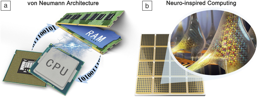
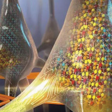
Figure 1. (a) The von Neumann architecture is employed in current computing devices, where the processing and memory units are separated and extensive shuffling of data between them is necessary. (b) Potential neuro-inspired device with unified computation and storage functions integrated in memory arrays. Phase-change materials (PCMs) hold the promise to achieve this goal. The sketch of PCM-based neurons is adapted with permission from IBM. Note: RAM, random-access memory; CPU, central processing unit.
Besides conventional digital computing tasks, analog computing is also being pursued, which is more efficient for object recognition, natural language processing, decision making, and other artificial intelligence (AI)-related tasks.Reference Xia and Yang2 The current achievements of AI applications are mainly driven by software programming,3 such as the machine learning algorithms that mimic the functions and topologies of neural networks in human brains. Despite the success of AI algorithms, such as the AlphaGo program designed to play the board game Go,Reference Silver, Huang, Maddison, Guez, Sifre, van den Driessche, Schrittwieser, Antonoglou, Panneershelvam, Lanctot, Dieleman, Grewe, Nham, Kalchbrenner, Sutskever, Lillicrap, Leach, Kavukcuoglu, Graepel and Hassabis4 they currently operate on conventional von Neumann digital-type computers, which consume a huge amount of electric power and spatial volume. All of these challenges are awaiting a fundamental change in computing hardware to increase the efficiency at reduced power consumption and chip dimensions.
Nonvolatile memory and neuro-inspired computing
In response to the increasing demand for data storage and processing power, nonvolatile memoryReference Wuttig5–Reference Pan, Gao, Chen, Song and Zeng8 (NVM) and neuro-inspired computingReference Mead9–Reference Zidan, Strachan and Lu12 (NIC) electronic devices that are highly compatible with the current complementary metal oxide semiconductor (CMOS) technology are being developed. NVM combines the advantages of the fast operation speed of DRAM/SRAM and the persistent storage (retained when powered off) of SSDs/HDDs, holding the promise to optimize and even unify all memory and storage units in one memory chip. NIC shifts the focus of processing-centric computing toward memory-centric computing, breaking the von Neumann barrier by making calculations in memory arrays (Figure 1b). Depending on the degree of biological resemblance to the human brain, NIC implementations can be categorized into different levels.Reference Sebastian, Le Gallo, Burr, Kim, BrightSky and Eleftheriou11
In addition to electronic NVM and NIC, photonic devices are also under active development. Although photonics is so far less technologically mature than electronics, optical systems can, in principle, offer a much higher bandwidth for data transfer.Reference Burr13 Therefore, all-optical supercomputers equipped with photonic NVM and NIC components may be the future of computing devices.
Among the emerging material candidates for NVMReference Wong and Salahuddin1 and NIC,Reference Xia and Yang2 phase-change materials (PCMs) are the most mature for large-scale production.Reference Hruska14
PCMs
PCMsReference Zhang, Mazzarello, Wuttig and Ma15–Reference Sun, Zhou and Ahuja21 are a special group of semiconductors, mainly comprising chalcogenides or antimonides. The flagship PCM is Ge2Sb2Te5Reference Yamada, Ohno, Akahira, Nishiuchi, Nagata and Takao19,Reference Yamada and Matsunaga22 (GST) that is currently being used in PCM chips, such as the recently released 3D Xpoint products,Reference Hruska14 serving as storage-class memories to bridge the performance gap between DRAM and SSDs. Together with GST, GeTe,Reference Chen, Rubin and Barton23,Reference Bruns, Merkelbach, Schlockermann, Salinga, Wuttig, Happ, Philipp and Kund24 Ag4In3Sb67Te26,Reference Matsunaga, Akola, Kohara, Honma, Kobayashi, Ikenaga, Jones, Yamada, Takata and Kojima25,Reference Iwasaki, Harigaya, Nonoyama, Kageyama, Takahashi, Yamada, Deguchi and Ide26 Ge15Sb85,Reference van Pieterson, van Schijndel, Rijpers and Kaiser27,Reference Ronneberger, Chen, Zhang and Mazzarello28 Sb,Reference Salinga, Kersting, Ronneberger, Jonnalagadda, Vu, Le Gallo, Giannopoulos, Cojocaru-Mirédin, Mazzarello and Sebastian29,Reference Zhang and Ma30 and Sc0.2Sb2Te3Reference Rao, Ding, Zhou, Zheng, Xia, Lv, Song, Feng, Ronneberger, Mazzarello, Zhang and Ma31,Reference Zewdie, Zhou, Sun, Rao, Deringer, Mazzarello and Zhang32 have been extensively studied and applied for electronic memories and processors, rewriteable optical discs, as well as photonic memories, processors, and even displays.Reference Burr13–Reference Hosseini, Wright and Bhaskaran48
The basic working principle of a PCM using the example of GST is shown in Figure 2. The contrast in electrical resistance (∼103) or optical reflectivity (∼30%) between a disordered amorphous state and an ordered crystalline state of the PCM is utilized to identify the logic states “0” and “1” through a weak voltage or laser READ pulse.Reference Wuttig and Yamada6 To RESET or erase the memory cell, a high-level and narrow voltage or laser pulse is applied to the crystalline GST, which heats up the memory cell above the melting temperature T melt of GST (∼900 K). A molten liquid state is reached and the subsequent rapid quenching of the liquid state results in an amorphous state. The RESET operation is typically rapid, finished over tens of picoseconds, but is power consuming and proper thermal insulation is compulsory to prevent heat loss.Reference Zhang, Mazzarello, Wuttig and Ma15
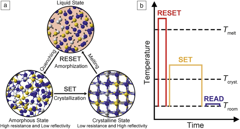
Figure 2. Working principle of phase-change materials for memory applications. (a) Ge2Sb2Te5 (GST); Ge, Sb, and Te atoms are rendered as white, yellow, and blue balls, respectively. The amorphous and crystalline states are characterized by high resistance/low reflectivity and low resistance/high reflectivity, respectively. To SET a memory cell, amorphous GST undergoes crystallization, while for RESET, crystalline GST is first melted and then the liquid is rapidly quenched, accomplishing the amorphization process. (b) The RESET and SET operations are triggered by applying voltage or laser pulses, which heat up GST to different temperature levels, either above the melting temperature (T melt) or in between the crystallization temperature (T cryst.) and melting temperature. The READ pulse is typically very weak, leading to little change in temperature.Reference Wuttig and Yamada6
To SET or write the memory cell, a medium level and longer duration voltage or laser pulse is applied to amorphous GST, which raises the local temperature above the crystallization temperature, T cryst., for fast crystallization (∼500–600 K). For GST devices, the SET time is of the order of tens of nanoseconds,Reference Zhang, Mazzarello, Wuttig and Ma15 with the stochastic nucleation process being the bottleneck. Nevertheless, this SET time limit can be drastically reduced to the subnanosecond regime either by applying a prepulse (where a 10-ns pulse of low voltage, such as 0.3 V, is applied for incubation of GST prior to the SET operation)Reference Loke, Lee, Wang, Shi, Zhao, Yeo, Chong and Elliott49 or by replacing GST with an alternative material such as the recently designed Sc0.2Sb2Te3 compound with an intrinsically short incubation time for crystal nucleation.Reference Rao, Ding, Zhou, Zheng, Xia, Lv, Song, Feng, Ronneberger, Mazzarello, Zhang and Ma31
In addition to binary storage, multilevel storage has been demonstrated to be feasible using PCM-based electronic and photonic devices.Reference Zhang, Mazzarello, Wuttig and Ma15,Reference Ríos, Stegmaier, Hosseini, Wang, Scherer, Wright, Bhaskaran and Pernice45 For example, in the electronic version, several partial RESET states can be obtained by adjusting the amplitude of the RESET voltage pulse (Figure 3a). A stronger pulse corresponds to a larger programming area and effective amorphous volume (indicated by black lines and red areas, respectively, in Figure 3b). The cell resistance changes as a function of the crystalline to amorphous volume ratio. Such a programming scheme is termed as iterative RESET.Reference Sebastian, Le Gallo, Burr, Kim, BrightSky and Eleftheriou11 This scheme suffers from the spontaneous structural relaxation of amorphous PCMs at ambient temperatures,Reference Raty, Zhang, Luckas, Chen, Bichara, Mazzarello and Wuttig50 causing resistance drift.Reference Ielmini, Lacaita and Mantegazza51 Iterative RESET serves as one of the two working modes for PCM-based neuro-inspired devices. The other one is termed as cumulative SET.Reference Sebastian, Le Gallo, Burr, Kim, BrightSky and Eleftheriou11 Instead of sending a strong SET pulse to fully crystallize the amorphous state, a train of weak SET pulses can be applied sequentially to the RESET amorphous state to obtain crystallization in a cumulative mode (Figure 3c). As shown in Figure 3d, the size of the programming area remains constant (within the black lines), while the effective amorphous volume changes in a random fashion (red areas) due to crystal nucleation, grain growth, and boundary shrinkage. Due to the stochasticity of crystallization, the cell resistance changes in a nonlinear way, and large fluctuations in cell resistance are found from pulse to pulse and cycle to cycle, causing variability issues.Reference Wright52
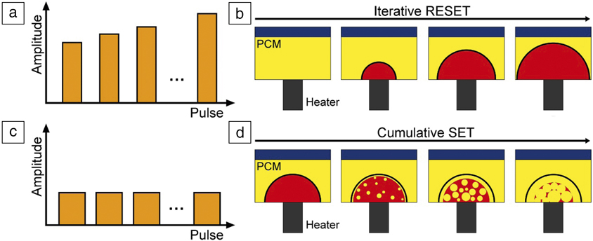
Figure 3. Working modes of phase-change materials (PCMs) for neuro-inspired computing (NIC). The amorphous and crystalline fractions are rendered yellow and red, respectively. (a, b) Iterative RESET programming. The RESET voltage pulses have a fixed width but a varied amplitude, leading to a gradual change in the size of programming areas (defined by the curved black line) as well as the effective amorphous volumes (red area). The resistance of the memory cell changes as a function of the crystalline to amorphous volume ratio. (c, d) Cumulative SET programming. The SET pulses are of the same width and with small amplitude, giving a constant size of programming area (within the black line). Cumulative SET operation is accomplished via incubation of crystal nuclei, their subsequent grain growth and parallel boundary shrinkage, giving rise to a nonlinear reduction in cell resistance with large stochasticity.
In this issue
The six articles in this issue of MRS Bulletin cover several important aspects of PCM fundamentals as well as electronic and photonic applications of PCMs. Recent breakthroughs in PCMs are summarized, and outlooks for future directions are presented.
The article by Wei et al.Reference Wei, Lucas and Angell53 presents an overview of the dynamics of liquid and supercooled-liquid PCMs. Liquid-to-liquid structural transitions, metal-to-semiconductor transitions, and other related phenomena are discussed in detail. Fragility of the liquid alloy, together with a new metallicity parameter proposed by the authors, are advocated as useful indicators for screening of PCM candidates that are most suitable for applications.
Pries et al.Reference Pries, Cojoracu-Miredin and Wuttig54 report recent progress on bonding mechanisms in PCMs, which is of fundamental importance for an understanding of the contrast in properties between the amorphous and crystalline states of PCMs. State-of-the-art atom probe tomography experiments for elucidating the bonding characteristics are thoroughly reviewed. Connections between metavalent bonding and kinetic properties of PCMs are also discussed.
The article by Sosso and BernasconiReference Sosso and Bernasconi55 highlights the development of machine learning-based interatomic potentials for large-scale molecular dynamics simulations at an accuracy level comparable to ab initio simulations. They use machine learning potentials to model the structural, dynamical, and thermal properties of the amorphous and liquid phases of the prototypical GeTe compound. The authors also pinpoint future challenges in applying machine learning techniques for addressing critical issues of PCMs.
Kim et al.Reference Kim, Nam, Burr and Kim56 focus on cycling endurance as a critical challenge that hinders further improvements in phase-change devices to rival DRAM. The current endurance limit is about 1012 write-erase cycles, which must be improved to 1015 or higher to meet the high-frequency memory requirements for data-intensive applications. The authors address various strategies for materials optimization, device engineering, and programming to break the cycle life bottleneck.
The Zhu et al.Reference Zhu, Ren and Song57 article in this issue discusses the ovonic threshold switching (OTS) phenomenon in amorphous chalcogenides, a field-assisted transition that makes an amorphous semiconductor switch from a highly resistive to a conductive state when a threshold voltage is reached. In addition to reviewing the theoretical models developed to elucidate this phenomenon, this article outlines the critical challenges in OTS materials and device performance optimization. In particular, the integration of OTS selectors and PCMs is discussed as a key ingredient in making high-density PCM chips.
Finally, Wright et al.Reference Wright, Bhaskaran and Pernice58 summarize recent breakthroughs in PCM-based photonic devices and integrated systems. They show how PCMs can be integrated into standard silicon photonics circuits. By utilizing the unique optical characteristics of PCMs, they show how binary and multilevel NVM, arithmetic and logic processing, as well as synaptic and neuronal mimics for NIC can be achieved for a photonics platform.
Future outlook
We anticipate rapid progress over the next decade toward production of electronic and photonic memory and neuro-inspired chips. However, further materials optimization and device engineering are needed to resolve several critical issues such as resistance drift, device variability, and power consumption. Progress in these areas is expected to benefit from the fundamental knowledge accumulated thus far, and in the future, at the atomic and electronic level for PCMs.
Acknowledgments
W.Z. acknowledges the support of the National Natural Science Foundation of China (61774123), 111 Project 2.0 (BP2018008), and the International Joint Laboratory for Micro/Nano Manufacturing and Measurement Technologies at Xi’an Jiaotong University. R.M. acknowledges funding from Deutsche Forschungsgemeinschaft within SFB 917 (“Nanoswitches”). E.M. is supported at Johns Hopkins University by US DOE-BES-DMSE under Grant No. DE-FG02–19ER46056.
Wei Zhang is a professor of materials science and engineering at Xi’an Jiaotong University, Xi’an, China. He received his bachelor’s and master’s degrees in physics from Zhejiang University, China, and his PhD degree from RWTH Aachen University, Germany. His current research interests include phase-change memory materials, first-principles materials design, and materials behavior at the nanoscale. He is supported by the university’s Young Talent Support Plan and the Youth Thousand Talents Program of China. His awards include the IFAM Young Scientist Award and the K.C. Wong Education Foundation Lecturer Award. Zhang can be reached by email at wzhang0@mail.xjtu.edu.cn.
Riccardo Mazzarello has been a professor of theoretical nanoelectronics and computational solid-state physics at RWTH Aachen University, Germany, since 2009. He is a computational physicist working in the fields of condensed-matter physics, mesoscopic physics, and materials science. His main research interests include phase-change materials, surface physics, and two-dimensional materials, which he investigates using ab initio methods based on density functional theory. Mazzarello can be reached by email at mazzarello@physik.rwth-aachen.de.
Evan Ma has been a professor of materials science and engineering at Johns Hopkins University since 1998. He has published approximately 340 archival papers, with around 36,000 citations (H index = 100), and presented approximately 235 invited talks at international conferences and seminars. His current research projects include local order and plasticity mechanisms in metallic glasses and high-entropy alloys, chalcogenide phase-change alloys, and in situ microscopy of small-volume materials exposed to mechanical, thermal, and environmental stimuli. He is an elected Fellow of the Materials Research Society, ASM International, and the American Physical Society. Ma can be reached by email at ema@jhu.edu.


