Hostname: page-component-848d4c4894-4rdrl Total loading time: 0 Render date: 2024-06-20T17:38:45.801Z Has data issue: false hasContentIssue false

Changes in the Density of States in a-Si:H with the Generation and Annealing of Light-Induced Defects

Published online by Cambridge University Press:  26 February 2011

K. Shepard
Affiliation:
Solid State Electronics Laboratory, Stanford University, Stanford, CA 94305
Z E. Smith
Affiliation:
Xerox Palo Alto Research Center, 3333 Coyote Hill Road, Palo Alto, CA 94304
S. Aljishi
Affiliation:
Max-Planck-Institut fuer Festkoerperforschung, Heisenbergstrasse 1, 7000 Stuttgart, West Germany
S. Wagnera
Affiliation:
Princeton University, Princeton, NJ 08544
Get access

Abstract

Through sub-bandgap absorption spectra and photoconductivity measurements of high-quality hydrogenated amorphous silicon (a-Si:H), changes in the electronic density of states with light-soaking and subsequent annealing are qualitatively described. Included is a more complete understanding of the role of deep defects as recombination centers. In this way, the simple power laws of Stutzmann, Jackson, and Tsai for the light-induced degradation of defect density and photoconductivity are. retained in the modified forms 
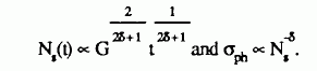
Evidence is also presented that the states closest to midgap, those states that act as effective recombination centers, are the first to anneal.

Type
Research Article
Copyright
Copyright © Materials Research Society 1988

Access options

Get access to the full version of this content by using one of the access options below. (Log in options will check for institutional or personal access. Content may require purchase if you do not have access.)

References

[1] Staebler, D. L., and Wronski, C. R., Appl. Phys. Lett 31,292 (1977)Google Scholar
[2] Stutzmann, M., Jackson, W. B., and Tsai, C. C., Phys. Rev. B 32, 23 (1985)CrossRefGoogle Scholar
[3] Lee, C., Ohlsen, W. D., and Taylor, P. C., in Materials Issues in Amorphous Semiconductor Technology, edited by D. Adler, Y. Hamakawa, and A. Madan, Volume 70, pp. 225229 (1986)Google Scholar
[4] Street, R. A., Phil. Mag. B 46, 273 (1982)Google Scholar
[5] Fritzsche, H., Proc. Int. Conf. on Stability of Amorphous Silicon Material, Jan. 28–30, 1987, Palo Alto, CA, AIP Conf. Proc. 157, 366–377 (1987)Google Scholar
[6] Aker, B. and Fritzsche, H., J. Appl. Phys. 54, 6628 (1983)CrossRefGoogle Scholar
[7] Vanecek, M., Kocka, J., Stucklik, J., Kozisek, Z., Stika, O., and Triska, A., Solar Energy Materials 8, 411 (1983)Google Scholar
[8] Taylor, G. W. and Simmons, J. G., J. Non-Crystalline Solids 8–10, 940 (1972)Google Scholar
[9] Rose, A., Concepts in Photoconductivity and Allied Problems (Krieger, Huntington, NY, 1978), pp. 2433 Google Scholar
[10] Slobodin, D., Aljishi, S., Schwarz, R., and Wagner, S., in Materials Issues in Applications of Amorphous Silicon Technology, Vol. 49, edited by Adler, D., Madan, A., and Thompson, M. J. (MRS, Pittsburgh, 1985), p. 153 Google Scholar
[11] Jackson, W. B. and Amer, N. M., Phys. Rev. B 25, 5559 (1982)Google Scholar
[12] Jackson, W. B., Kelso, S. M., Tsai, C. C., Allen, J. W., and Oh, S.-J., Phys. Rev B 31, 5187 (1985)CrossRefGoogle Scholar
[13] Smith, Z E., Chu, V., Shepard, K., Aljishi, S., Slobodin, D., Kolodzey, J., Wagner, S., and Chu, T. L., App. Phys. Lett. 50, 1521 (1987)Google Scholar
[14] Smith, Z E. and Wagner, S., Mat. Res. Soc. Symp. Proc. 95, 551 (1987)Google Scholar
[15] Moddel, G., Anderson, D. A., and Paul, W., Phys. Rev. B 22, 1918 (1980)CrossRefGoogle Scholar