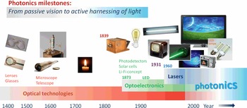

1.1 From Passive Vision to Active Harnessing of Light
Light plays a major role in our perceptual cognition through vision, which occurs in the very narrow spectral range of electromagnetic radiation from approximately 400 nm (violet) to approximately 700 nm (red), whereas the whole wealth of electromagnetic wavelengths extends from picometers (gamma rays) to kilometers (long radiowaves) and beyond. In the early stages of technology, humans strived for enhancement of visual perception. Major highlights are: the invention of eye glasses (Salvino D’Armate, Italy, at the end of the thirteenth century); the invention of the microscope c.1590 by two Dutch spectacle makers, Zacharias Jansen and his father Hans; and the invention of the telescope in 1608 by Hans Lippershey, also a Dutch eyeglass maker (Figure 1.1). These devices only enhanced our passive vision by means of light coming from the sun or another source, e.g., a candle or an oven, and scattered toward our eyes. At that time no attempt had been made to generate light other than through the use of fire, or to store images in any fashion. Much later, in 1839, Louis Daguerre introduced the first photocamera (daguerreotype) in which a light-sensitive AgI-coated plate was used for image recording. This was the first manmade optical processing device. In 1873–1875, Willoughby Smith in the USA and Ernst Werner Siemens (Siemens Reference Siemens1875) in Germany described the remarkable sensitivity of a selenium film conductivity to light illumination, thus creating a basis for photoelectric detectors. Very soon after, in 1880, using a selenium plate as a photodetector, Alexander Bell in the USA ingeniously demonstrated wireless optical communication over 200 m using a sunbeam modulated by a microphone membrane (Bell Reference Bell1880). The modulated signal was received by a photodetector, converted into an electric signal and eventually into acoustic vibrations by a telephone. Later, during World War I, this idea was implemented in a communication across a few kilometers for military purposes, using modulated incandescent lamp radiation. This is the approach to wireless optical communication that has more recently gained the notation “Li-Fi” (light fidelity). For a practical, far-reaching implementation of optical communication, reliable light sources with fast modulation were needed. Notably, at this time, Charles Fritts (Reference Fritts1883) in New York developed a solar cell with 1% efficiency using selenium on a thin layer of gold, thus introducing the possibility of industrial-scale photovoltaics.

Figure 1.1 Milestones of photonics technologies.
Systematic experiments with electric gas discharge resulted in the first electric gas lamps being introduced in Europe and the USA around the early 1900s. These were the first devices directly converting electricity into light without heating. The emergence of television (TV) in the USA in 1923–1930 was allowed by the iconoscope, invented by Vladimir Zworykin (1988–1982), a brilliant Russian mind, at the time working at Westinghouse and RCA. His TV transmitter and receiver were both based on cathode ray tubes. The advent of the TV marked the beginning of the optoelectronic era in which humans attempted to transmit, receive, store, and reproduce optical data using electrical processes.
Notably, in the same period the light-emitting diode was invented (see Zheludev Reference Zheludev2007). In 1907, in a brief 22-line letter to the Electric World editor, Henry J. Round reported on curious observations of visible light starting from 10 V applied to a crystal piece of SiC, at that time referred to as carborundum (Round Reference Round1907). This preliminary report was not noticed at the time, and in the period 1928–1933 Oleg Losev (Losev Reference Losev1928) from Nizhniy Novgorod (Russia) performed a systematic study of electroluminescent properties of metal–semiconductor junctions with a carborundum crystal, thus marking the emergence of semiconductor light-emitting diodes. His works were published in Philosophical Magazine and Physikalische Zeitschrift. Sadly, Oleg Losev died in 1942 at the age of only 39 in Leningrad, suffering from severe hunger during the time of the fascists’ siege. His works were forgotten for decades. Only much later, in 1961, were the modern generation of III–V LEDs reported by J. R. Biard and G. Pittman from Texas Instruments (USA), and the first visible LED was made by N. Holonyak at General Electrics in 1962.
The first lasers appeared in 1960 in the USA (solid-state lasers with optical pumping, T. H. Maiman; P. Sorokin and M. Stevenson; a gas discharge laser, A. Javan, 1960). The term LASER (light amplification by stimulated emission of radiation) was introduced by G. Gould, the author of the first patent of an optically pumped laser (1957). In 1962–1963 the first semiconductor laser diodes was reported (USA: R. Hall et al.; M. Nathan et al.; T. Quist et al.; USSR: V. S. Bagaev et al.). Semiconductor lasers enabled modern fiber optical communication, which now reaches almost every building and home. These lasers have also made it possible to develop laser disk (CD-ROMs, and also rewritable CDs) systems for data processing and audio/video recording/reproduction. Owing to double heterostructures with quantum wells, modern semiconductor diodes have achieved unparalleled wall-plug efficiency levels exceeding 50%, the exceptionally high direct conversion of electric current into light.
Thanks to quantum well InGaN semiconductor structures, blue LEDs have made a revolutionary step toward all-solid-state lighting. The detector components have also made great progress, with outstanding performance of familiar charge-coupled device (CCD) arrays in modern digital photo- and video-cameras. Progress in semiconductor optoelectronics was marked by the three Nobel prizes awarded to Zh. Alferov and R. Kremer (2000, double heterostructures), W. S. Boyle and G. E. Smith (2009, CCD array), and I. Akasaki, H. Amano, and S. Nakamura (2014, blue LEDs).
To emphasize the merging of optics, optoelectronics, and laser technologies, the notion of photonics was coined a couple of decades ago. Photonics embraces all technologies and devices in which electromagnetic radiation of the visible, infrared, and ultraviolet ranges is harnessed for our needs.
1.2 What is Nanophotonics?
Nanophotonics makes use of a wealth of size-dependent phenomena arising when space and matter feature confinement at a nanoscale. First, since the wavelength of electromagnetic radiation used in photonics is of the order of 1 µm in air and reduces to a few hundreds of nanometers in dielectric and semiconductor media, fractioning of matter and space on the scale of the order of 100 nm changes conditions for electromagnetic radiation propagation and the related lightwave confinement phenomena appear. Light–matter interaction in photonics mainly reduces to the interaction of electromagnetic radiation with electrons in atoms, molecules, and solids. Therefore, optical absorption and emission rates and spectra are defined to a large extent by electron properties of the matter. Owing to the wave properties of electrons featuring de Broglie wavelength of the order of 10 nm in semiconductors, the confinement of matter on this scale gives rise to a number of size-dependent phenomena referred to as quantum confinement effects. The term “quantum” here highlights that these phenomena result from quantum mechanical consideration.
Nanophotonics studies light–matter interactions at the nano scale and makes use of the aforementioned lightwave confinement and electron confinement phenomena in various structures and devices. Each of the two types of the confinement effects suggest a number of ways to improve and/or modify the parameters of existing optoelectronic devices, including light-emitting diodes, laser diodes, solid-state lasers, solar cells, and optical communication circuitry. Because of the different scales of lightwave and electron confinements, both groups of phenomena can be applied simultaneously in the same device, as often occurs, e.g., in modern semiconductor lasers.
This book represents the authors’ attempt to introduce engineers and researchers to the realm of nanophotonics. It is broken down into two parts: Part I, Basics; and Part II, Advances and Challenges.
Part I presents the minimal tutorial description of electron and lightwave properties in nanostructures and the basic physical principles of nanophotonics, namely: properties of electrons in various potential wells (Chapter 2); electron properties of semiconductor nanostructures (Chapter 3); properties of electromagnetic waves under size confinement (Chapter 4); modification of spontaneous emission rates in nanostructures (Chapter 5); principles of optical gain and lasing (Chapter 6); and energy transfer phenomena (Chapter 7). The content of this part implies knowledge of solid-state theory and optics at the undergraduate and introductory graduate levels. The interested reader can find more specialized works (e.g., Miller [Reference Miller2008], Gaponenko [Reference Gaponenko2010], Joannopoulos et al. [Reference Joannopoulos, Johnson, Winn and Meade2011], Klingshirn [Reference Klingshirn2012], Novotny and Hecht [Reference Novotny and Hecht2012], and Klimov [Reference Klimov2014]) if they wish to dive deeper into the basics of nanophotonics. In Part I, references to the plentiful original publications are reduced to the reasonable minimum while focusing at the physical essence of the phenomena involved and experimental prerequisites for their implementation.
Part II describes current advances of applications of the principal electron confinement and light confinement phenomena in various practical devices. This part of the book covers applications of nanostructures in lighting (Chapter 8); lasers (Chapter 9); optical communication circuitry (Chapter 10); and photovoltaics (Chapter 11). Each of these chapters ends with a list of challenges the designers face, and a tentative forecast for the near-future progress. The very last chapter, Chapter 12, explores emerging nanophotonics. Here, new trends in nanophotonics are traced that offer promise of new photonic components (densely integrated optical chips, subwavelength lasers, various sensors, bioinspired and biocompatible devices) and technological platforms (colloidal photonics, silicon photonics). In Part II, we attempt to overview the principal achievements in nanophotonic devices, which makes it necessary to extend the list of references to the original publications.
The style and materials covered meet the level of graduate students. Advanced readers can skip Part I and consider only Part II. Since students in engineering may lack an optical background, all necessary introductory data from semiconductor optics, material optical properties, light propagation in inhomogeneous media and nanostructures are included. Challenges discussed in the textbook show modern trends and emphasize that nanophotonics is an open and active field bordering optical engineering, materials science, electronics engineering, and sometime colloidal chemistry and even biophysics.
This book highlights the basic principles of nanophotonics and their successful implementation in photonic devices, and will be a good companion book for a number of specialist publications devoted to specific types of optoelectronic devices that have been published lately: Chow and Koch (Reference Chow and Koch2013), Liu (Reference Liu2009), Cornet et al. (Reference Cornet, Léger and Robert2016), Schubert (Reference Schubert2006) with the summarized and emphasized role of nanostructures in existing and emerging photonics.