Introduction
Resistive switching (“memristive”) in thin-film devicesFootnote * under electrical stress (i.e., voltage or current bias) has been observed in a variety of material systems, and different physical mechanisms have been identified that contribute to this effect. In this article, we review the prospective applications of the resistive switching phenomenon. Recent reviews of this topic can be also found.Reference Ha and Ramanathan1–Reference Strukov, Likharev, Waser and Waser5 Note that material systems and physical mechanisms are not discussed in this article but will be reviewed in the articles in this issue.
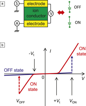
In its simplest form, a memristive device consists of three layers: top and bottom (metallic) electrodes and a thin film (Figure 1). By applying a voltage bias across the electrodes of such a device, the electrical conductivity of the thin film can be changed reversibly and retained for a sufficiently long time between a highly conductive (ON) state and a highly resistive (OFF) state. Very often, the switching could be continuous between these two extreme states so that intermediate states are also possible. Figure 1b schematically shows the I–V curves for a bipolar switching device. For a detailed classification of the observed switching behaviors, see Figure 1 of the Yang et al. article in this issue. In bipolar devices, an electrical stress of opposite polarity is required to switch the device between ON and OFF states. Note that the particular shape of the I–V curve in the ON/OFF states might vary and will depend on the additional layers integrated in the device stack. In general, nonlinearity of the ON state is required for most of the applications (e.g., to suppress leakage current in crossbar memories) and is achieved by either intrinsic properties of the device (e.g., internal tunnel barrier gap or Schottky barrier) or explicit integration in the device stack of a tunnel barrier (diode, or specific structures such as an ovonics threshold switch) (see the article by Raoux et al. in this issue). Also, Figure 1 does not show the so-called “forming step,” which might be required for metal-oxide, solid-state electrolyte, and organic devices before the devices can be switched reversibly (see the articles by Yang et al., Lu et al., and Lee et al. in this issue). Such a forming step is essentially a one-time application of relatively large voltage bias and can be eliminated in properly engineered devices.
(a) Device structure and (b) typical hysteretic I–V behavior for bipolar switching, shown schematically. Panel (a) also shows circuit notation for the resistive switching device in the context of digital applications.
It is expected that with the trend of aggressive downscaling of commercial electronic devices into the nanoscale regime, quantum mechanical effects will become steadily more important. This trend will lead to a change of paradigm (i.e., future nanoelectronic devices exploiting electron tunneling and/or spin transport will rely on the fundamental laws of quantum mechanics rather than on classical electrodynamics). In particular, complex oxide tunnel junctions involving a ferroelectric barrier with a high spontaneous polarization and two ferromagnetic electrodes offer an ideal platform for investigating the interplay between electrical polarization and tunneling magnetoresistance in a controlled manner for future non-volatile memories and neural network applications (see the article by Tsymbal et al. in this issue).
Crossbar digital memories
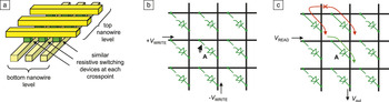
The most straightforward application of the resistive switching phenomenon is in digital memories. In this context, passive crossbar memories, which are implemented with mutually perpendicular layers of parallel wires (electrodes) with integrated thin-film devices at the crosspoints (Figure 2a), have the best scaling prospects. The basic operation of crossbar memories can be explained using simplified equivalent circuits shown in Figure 2c. In the ON state representing binary 1, the memristive device is essentially a diode, so that the application of voltage V t < V READ < V ON to one (horizontal) nanowire leading to the memory cell gives a substantial current injection into the second wire (Figure 2c). This current pulls up voltage V out that can now be read by a current sense amplifier. (Alternatively, the current can be sensed directly by keeping the potential constant at the vertical wire with a virtual ground scheme.Reference Xu, Dong, Jouppi and Xie6) To have low currents at voltages above ∼V t, the diode property prevents parasitic currents, which might be induced in other ON-state cells by the output voltage (see the red line in Figure 2c). In the OFF state (binary zero), the crosspoint current is very small, giving a nominally negligible contribution to output signals at readout. In order to switch the cell into the ON state, the two nanowires leading to the device are fed by voltages +V WRITE and −V WRITE with V WRITE < V ON < 2V WRITE. The left inequality ensures that this operation does not disturb the state of “semi-selected” devices contacting just one of the biased nanowires. The write 0 operation is performed similarly using the reciprocal switching with threshold V OFF.
Passive crossbar array: (a) A schematic of the structure and the idea of (b) writing and (c) reading a particular bit. The green arrow in (c) indicates the currents via the selected device, while red arrows show the leakage current (adapted from Reference Reference Strukov, Likharev, Waser and Waser5).
Note that the memory cell of conventional (active) memories includes a transistor that provides “select” functionality (i.e., the ability to select a given cell in the array). The density scaling of such memories is therefore, at best, limited by the scaling of the transistor. The transistor has two critical dimensions and therefore cannot be scaled aggressively. On the other hand, there might be only one critical dimension (i.e., film thickness) for memristive devices. On the contrary, in passive crossbar memories, each crosspoint device combines memory and select functionality so that the footprint of a memory cell is defined by the overlap area of the electrode (crossbar) wires and is close to 4F wire2, where F wire is the crossbar wire pitch. The pitch could be made as small as a few nanometers, for example, by using emerging nanoimprint technology.9 Moreover, if fabrication of memristive devices does not require high temperatures, multiple cells can be stacked monolithically, resulting in even further downscaling of the effective footprint.
Naturally, the memory density will also depend on peripheral circuitry, which is required to facilitate write and read operations (not shown on Figure 2b–c). These include decoders to select proper rows or columns, drivers to apply specific voltages, and sensing circuitry to read out the device state. For an N × N crossbar array, such peripheral area overhead is roughly proportional to N*logN, while useful area scales such as N 2 and, therefore, having larger crossbar arrays helps to improve the density of the memory. On the other hand, increasing N leads to larger readout delays, voltage drop across crossbar wires, and, most importantly, leakage currents via semi-selected devices (Figure 2c). This is why implementing strong nonlinearity in the I–V curve is one of the most important goals for the resistive switching devices in the context of passive crossbar memories.
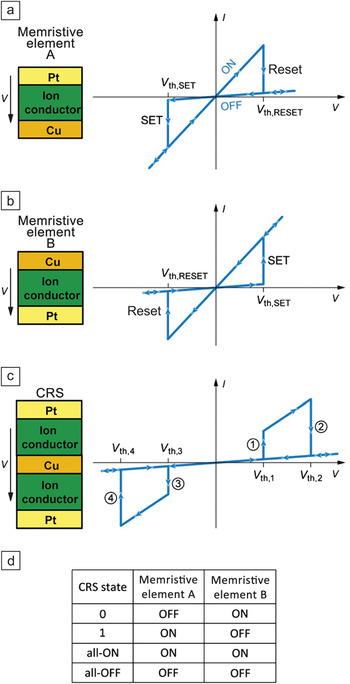
Linn et al.Reference Linn, Rosezin, Kugeler and Waser8 has recently proposed an interesting approach to alleviate the problem of leakage currents, which does not require nonlinearity in the ON state (Figure 3). The main idea is to combine two bipolar resistive switch elements, which are connected in series, as shown in Figure 3, in a memory cell, referred to as a complimentary resistive switch (CRS). There are four possible states in a CRS, but only two high resistive states are used to represent binary 0 and 1, see Figure 3. This ensures that all semi-selected CRS devices in a crossbar array could effectively always be in the OFF state, and the leakage current is minimal. However, the tradeoff for this is a more complicated and destructive read operation. The read operations could be performed via applying a positive voltage sweep across the CRS device (Figure 3). The CRS will switch to the intermediate all-ON state only if it was initially in the 1 state. Detecting whether such an all-ON state was present during a destructive voltage sweep is used to distinguish between 0 and 1 values stored in a CRS device for read operation.
A complementary resistive switch: Specific hysteretic I–V behavior for the (a) top, (b) bottom, and (c) combined devices and (d) corresponding table showing mapping of resistive states to binary memory values (adapted from Reference Reference Linn, Rosezin, Kugeler and Waser8).

According to the international technology roadmap of semiconductors (ITRS), crossbar memory is a potential candidate to become a universal memory, which would combine the best characteristics of other types of memories.9 This is based on numerous recent experimental demonstrations showing, for instance, operational devices with few-nanometer dimensions, sub-nanosecond write speed, year-long retention, large ON/OFF ratio, and high >1013 endurance (i.e., cycling between ON and OFF states). Examples of such devices and prospects of combining all these properties in a single device are discussed in the articles in this issue. It is worth mentioning that a large integration density would require improvement of yield and reducing variations in the switching behavior. It seems that these cannot be eliminated completely or reduced to the typical levels of the conventional technology so that novel defect and fault tolerant approaches will be required (see Reference Reference Strukov, Likharev, Waser and Waser5 for more discussion of this point).
Digital logic
The development of passive crossbar memories would be beneficial to a certain class of digital logic systems—so-called reconfigurable field programmable arrays (FPGA).Reference Strukov, Likharev, Waser and Waser5 FPGAs, which combine some of the best properties of microprocessors and application-specific integrated circuits (such as cost-effectiveness of the former and the ability to be customized for a particular task of the latter), are becoming increasingly attractive for a variety of applications. Conceptually, FPGA can be thought of as a large number of logic gates with a connectivity pattern among the gates being kept in on-chip memory. For example, a specific bit of memory might control whether two wires (e.g., input of a gate and output of another) are electrically connected. The operation of the FPGA, therefore, can be broken into two consecutive stages: first, a particular computation task is mapped to the FPGA structure by writing a specific connectivity pattern in its memory. During the second (much longer) stage, the connectivity pattern is fixed, and FPGA runs a specific task with a programmed circuit.
The use of memristive devices might eliminate the main inefficiency of FPGAs—large overhead associated with programmability. Indeed, FPGA memory is implemented as static RAM or flash memory and typically consumes a large area of the chip—on the order of 50%–90%.Reference Strukov, Likharev, Waser and Waser5 In this context, a significant improvement in density (more than 10× over conventional FPGAs) might be achieved by implementing programmable connections between complementary metal oxide semiconductor (CMOS) gates with memristive devices (Figure 4b). In such hybrid CMOS/memristor circuitry, programmable connections are lifted into upper metallization layers, therefore drastically reducing FPGA overhead. In a more aggressive approach, the programmable connections also implement some of the logic gate functionality (Figure 4c). For example, the nonlinearity of the memristive devices may be used to implement diode-type logic, while a CMOS subsystem is used for signal restoration and inversion (Figure 4d). Simulation results showed that the latter approach might improve the density of the FPGA by a factor of 100.Reference Strukov, Likharev, Waser and Waser5
Hybrid complementary metal oxide semiconductor (CMOS)/memristor field programmable gate arrays (FPGAs): (a) A schematic of the hybrid circuitry and two FPGA implementations. A top view of (b) Hewlett Packard Laboratory23 and (c) Stony Brook UniversityReference Strukov and Likharev24 versions with (d) the equivalent circuit for a single NOR gate for the latter concept. Only a few crossbar nanowires and ON-state memristive devices participating in a specific example are shown on panels (b) and (c) for clarity.

Borghetti et al.Reference Borghetti, Snider, Kuekes, Yang, Stewart and Williams10 recently demonstrated a very different approach of using memristive devices in digital logic circuits—material implication logic. As shown in Figure 5, p and q denote binary states in which memristive devices P and Q could be configured, respectively, and it is assumed that the OFF (ON) state of the device represents binary 0 (1). The formula q’←p IMP q, which denotes implication logic operation and equivalent to q’ (NOT p) OR q, is implemented by simultaneously applying specific voltage pulses (“clock signal”) to the P and Q devices. With appropriately chosen voltage biases (V COND and V SET) and a value of load resistance (R G), the state of device P in the circuit in Figure 5a would change based on the original states of the devices P and Q, while the state of device Q will not be disturbed. More specifically, when the clock signal is applied, the resistive states of P and Q dictate the voltage on the common electrode and, as a result, the bias across device Q. In the case when device Q is in the OFF state, such a bias is always larger than that required to switch the device to the ON state. However, if device Q is originally in the ON state, the bias across Q is large enough to switch it to the OFF state only when device P is also in the ON state. The resulting logic operation is described in Figure 5, which is equivalent to implication operation.
Material implication logic: (a) Equivalent circuit, (b) corresponding truth table, and (c) experimental data. The blue and red curves on panel (c) show the voltages applied and the absolute value of the currents read at devices P and Q before and after the logical implication operation (IMP) voltage pulses. The measured low- and high-current values reproduce the IMP truth table (adapted from Reference Reference Borghetti, Snider, Kuekes, Yang, Stewart and Williams10).

The salient property of material implication logic is that the result of the logic operation is naturally stored as a resistance state in a nonvolatile memristive device. Such unique properties of material implication logic and the density advantages of memristive devices enable extremely high bandwidth computing. The nonvolatility of the memristive devices is also appealing in the context of energy scavenging devices, because memristive circuits can work with intermittent power supply. However, one of the challenges in material implication logic is the requirement of fast switching speed and high endurance of memristive devices, because the devices have to be switched every time the logic operation is performed. This is unlike the hybrid FPGA circuits, in which very low endurance (<100) and slow switching speed would be acceptable. The requirement for variations and yield are slightly better in hybrid FPGA circuits as compared to the crossbar memories. The simulation results showed that up to 20% of defective (stuck-on-OFF state) memristive devices can be tolerated in hybrid FPGA circuits compared to ∼1% in digital memories.Reference Strukov, Likharev, Waser and Waser5
Artificial neural networks
The idea of using resistive switching devices in artificial neural networks (ANN) has a long history and can be traced back to at least 1960.Reference Widrow11 This early work, however, was largely overlooked, mainly due to the emergence of the first successful digital microprocessor just years later, which would become a dominating platform for computing. Other significant developments in this context were in thin-film tungsten oxideReference Thakoor, Moopenn, Daun and Thakoor12 and a-Si:H device memristors,Reference Holmes, Gibson, Hajto, Murray, Owen, Rose and Snell13 but the results were not encouraging enough to render further investigations. More recently, the topic had been revived by titanium dioxide memristor publicationsReference Yang, Pickett, Li, Ohlberg, Stewart and Williams14 and further milestones, such as demonstration of spike time dependent plasticity (STDP)Reference Jo, Chang, Ebong, Bhadviya, Mazumder and Lu15, Reference Kuzum, Jeyasingh, Lee and Wong16 and short- and long-term potentiation in resistive switching devices.Reference Ohno, Hasegawa, Tsuruoka, Terabe, Gimzewski and Aono17 Today, the motivation behind the development of ANN comes from the fact that the mammalian brain still remains much more efficient (in power and processing speed) for a number of computational tasks, such as pattern recognition and classification, as compared to conventional computers, despite the exponential progress in the performance of the latter during the past several decades.
In the simplest abstract model, ANN can be represented by a graph with nodes corresponding to neurons and graph edges that correspond to synapses (Figure 6b). In parallel, each node processes input information from the preceding nodes and then passes it to the next layer of nodes. For example, the node processing could involve summation of input signals, with each scaled by the corresponding edge weights, followed by a specific threshold function of the node. Given a particular structure of the ANN, the functionality is defined by synaptic weights, which are adjusted during the learning process. In order to match human brain complexity, there should be on the order of 1011 nodes, with every node connected to 104 others on average, or equivalently, about 1015 edges. It is because of such high complexity, connectivity, and intrinsically massive parallel information processing that mimicking biological neural nets is very challenging, while the performance of the software emulating ANN or even customized developed hardware fall short by many orders of magnitude to that of biological counterparts.
Neural networks: (a) A phase contrast image of a cultured hippocampal neural net (reprinted with permission from Paul De Koninck, Laval University), (b) the corresponding abstracted graph-based model, and (c) the main idea of hardware implementation with complementary metal oxide semiconductor (CMOS)/memristor circuitry. Panels (b–c) are adapted from Reference Reference Strukov4.
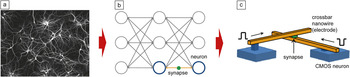
The development of the resistive switching device technology may change the situation dramatically. The structure of the ANN (Figure 6b) maps naturally on the hybrid CMOS/memristor concept (Figure 4a), with CMOS implementing neurons, the crossbar wires replacing axons and dendrides, and memristive devices acting as artificial synapses (Figure 6c). Note that in this case, it would be more appropriate to replace a one-way switch in the circuit symbol (inset of Figure 1a) by a variable resistor so that the conductance of the memristive devices represents the synaptic weight or its strength. Crude estimates have shown that the circuits with ultimately scaled CMOS technology and sub-10 nm scale memristive devices could challenge the complexity and connectivity of the human brain.Reference Likharev18
Given a very large number of synapses, any practical implementation of an artificial network should allow the weights to be updated in parallel, otherwise the learning process would be too slow. The primary mechanism for efficient learning in biological networks was postulated in 1949 by Hebb,Reference Hebb19 who noticed that the change in synaptic weight depends on the relative timing of pulses from its pre- and post-synaptic neurons. The weight strengthens if two neurons are activated simultaneously, and it weakens when they are active separately. The analog properties of memristive devices allow for the efficient mimicking of Hebbian learning in ANN (Figure 7).Reference Jo, Chang, Ebong, Bhadviya, Mazumder and Lu15 The trick is to find an appropriate shape and duration of the voltage pulses for the post- and pre-synaptic neurons to be used for Hebbian learning.Reference Kuzum, Jeyasingh, Lee and Wong16, Reference Linares-Barranco and Serrano-Gotarredona20 For example, for a metal oxide device with I–V characteristics shown in Figure 1, the temporal overlap between properly chosen pre- and post-synaptic pulses should result in a positively (negatively) applied voltage across artificial synapse for positive (negative) relative timing between these signals.
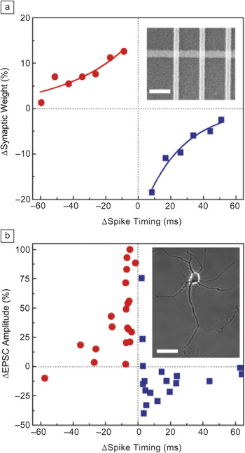
Demonstration of spike time–dependent plasticity in (a) artificial and (b) biological synapses. Insets for panels (a) and (b) show scanning electron microscope images of a fabricated memristor crossbar array (scale bar: 300 nm) and a phase contrast image of a hippocampal neuron (scale bar: 50 μm), respectively. The red circles and blue squares indicate the positive and negative changes, respectively, to (b) synaptic weight and (a) memristor weight or conductance. (Adapted from Reference Reference Jo, Chang, Ebong, Bhadviya, Mazumder and Lu15.)
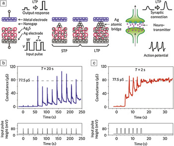
The work by Ohno and colleagues goes one step further.Reference Ohno, Hasegawa, Tsuruoka, Terabe, Gimzewski and Aono17 In previous work,Reference Jo, Chang, Ebong, Bhadviya, Mazumder and Lu15, Reference Kuzum, Jeyasingh, Lee and Wong16 the synaptic weight is changed only if a sufficiently high bias is applied across it. On the other hand, studies of biological synapses show two distinct modes—short-term plasticity (STP), lasting less than a few seconds, and long-term potentiation (LTP), which could persist for many hours. The synaptic weight becomes permanent (i.e., long-term memory is formed) only after repetitive reinforcement with overlapping pre-synaptic and post-synaptic pulses, while synaptic weight after single reinforcement decays quickly over time. Using silver sulfide thin-film devices (e.g., see the article by Lu et al. in this issue), both STP and LTP were demonstrated to coexist in one device (Figure 8).Reference Ohno, Hasegawa, Tsuruoka, Terabe, Gimzewski and Aono17 The two modes of operation were attributed to the fact that small, possibly atomically thick, silver filaments are unstable and dissolve rapidly even if no bias is applied. On the other hand, large filaments formed as a result of repetitive potentiation are more stable and can persist for a longer time.
Inorganic synapse showing short-term plasticity (STP) and long-term potentiation (LTP), depending on input-pulse repetition time. (a) Schematics of an Ag2S inorganic synapse and the signal transmission of a biological synapse. When the precipitated Ag atoms do not form a bridge, the inorganic synapse works as STP. After an atomic bridge is formed, it works as a LTP. In the case of a biological synapse, frequent stimulation causes long-term enhancement in the strength of the synaptic connection. (b–c) Change in the conductance of the inorganic synapse when the input pulses (V = 80 mV, W = 0.5 s) were applied with intervals of (b) T = 20 s and (c) 2 s. The conductance of the inorganic synapse with a single atomic contact is 2e2/h (= 77.5 μS), where e is an elementary charge, and h is Planck’s constant. The figure is adapted from Reference Reference Ohno, Hasegawa, Tsuruoka, Terabe, Gimzewski and Aono17.
It should be noted that for ANN systems, the density of the memristive devices is the most important property. Moderate endurance should be sufficient for implementing a learning process, and massive parallelism of the ANN might compensate for the slow switching speed. Also, ANNs are much more resilient to variations in synapses and neurons. For example, it could operate even in the presence of a large number (up to 90%) of bad (stuck-on-ON or stuck-on-OFF states) devicesReference Likharev18 and is quite tolerant to variations in the switching behavior.Reference Snider21
Summary
The development of thin-film resistive switching device technology should greatly benefit digital memory and logic circuits and may, for the first time, enable large-scale bioinspired neuromorphic circuits. The most critical issues at the moment are yield, reproducibility, and viable integration with conventional complementary metal oxide semiconductor technology. The authors are optimistic that these challenges could be addressed in the near future due to the large-scale investments of major semiconductor companies in fabrication technology, progress in understanding the physical phenomena behind resistive switching, and continuing advances in materials science and engineering.
Acknowledgments
D.B.S. would like to acknowledge the support of the National Science Foundation grant CCF-1028336 and useful discussions with John Carruthers and Konstantin Likharev.