


Atomic and molecular structure
Experimentalists discover nature’s secrets by measuring and reporting the properties of matter. Theorists explain these properties and attempt to predict new properties. This is similar to the cartoon depicting three cavemen discussing the invention of the wheel. The experimentalist says, “To be honest, I never would have invented the wheel if it were not for Urg’s groundbreaking theoretical work with the circle!” Condensed-matter theorists naturally side with Urg, who, as shown in the cartoon, makes several unsuccessful attempts before he finally discovers the right idea for the wheel.
One of the most important concept in all of science is that macroscopic matter is composed of atoms. However, even at the beginning of the 20th century, this concept was not universally accepted by the scientific community, even though the ideas about atoms were first proposed by the ancient Greeks. Einstein’s PhD thesis on measuring the size of sugar molecules in 1905 helped verify the fact that molecules and atoms exist.Reference Einstein1 Later, when scientists tried to explain the properties of atoms, they realized they needed to invoke quantum theory. They relied partially on the example of Einstein’s (1921) Physics Nobel Prize winning work—an explanation of the photoelectric effect. This study showed that light could be viewed as a particle or wave, which was an important concept for establishing quantum theory.
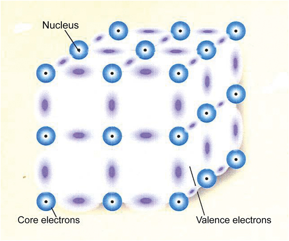
Our current picture of an atom can be modeled as a positive nucleus surrounded by electrons that are held close to the atom (core electrons) and outer valence electrons that can participate in chemical reactions to form molecules or solids. For example, in the case of silicon, the nucleus contains 14 positive charges with 10 core electrons, so the charge on the core is essentially +4. The core structure does not change much when building solids from atoms since the core basically remains intact.
The objective of condensed-matter physics is to explain the properties of valence electrons and the way they must be arranged to form a solid and to give the resulting system its properties. Quantum mechanics shows that the properties of particles are often described in terms of probabilities. For example, only the probability associated with finding an electron precisely in a specific position can be predicted. An electron position precisely at a specific point cannot be determined.
In 1929, P.A.M. Dirac, who contributed greatly to the development of quantum theory, posed what is sometimes referred to as Dirac’s challenge. He stated that “the underlying physical laws necessary for a large part of physics and all of chemistry are completely known, and the difficulty is only that the exact application of these laws leads to equations much too complicated to be soluble.”Reference Dirac2 This article essentially describes the ways in which Dirac’s challenge has been answered in this field.
Structure and classification of solids
Early research involving quantum theory concentrated on the optical properties of gases, because, in this case, one could deal with individual atoms. This was a critical factor in establishing quantum theory and explaining the properties of atoms. For example, in the absorption spectra for gaseous atoms, the spectral lines are very narrow and can be explained in terms of transitions of electrons between different atomic levels. The separation of the two Na D lines in optical studies on sodium is about 20 meV. In contrast, for the room-temperature reflectivity spectra of three different semiconductors as a function of energy shown in Figure 1,Reference Cardona and Greenaway3 the width of the line drawing the curve is larger than the separation of the Na D lines (the scale is eV), making these broad features difficult to interpret.
Room-temperature reflectivity of HgTe, CdTe, and ZnTe samples show the broad absorbances in solids that were difficult to interpret with early quantum theories. Reprinted with permission from Reference Reference Cardona and Greenaway3. © 1963 American Physical Society.

When scientists started to classify solids in the 1800s, they first examined their mechanical behavior, and to determine relative hardness, they took one solid and scratched it on another. They repeated the exercise with a series of solids to determine which was the hardest and developed a hierarchy of hardness. In 1812, Friedrich Mohs used data of this kind to introduce the Mohs scale for mineral hardness and arbitrarily gave diamond, the hardest material we know, the value 10.
After this, research concerning solids became more sophisticated, and scientists began classifying solids in terms of their chemical composition. The discovery of x-rays allowed another classification where researchers could experimentally measure the periodic atomic structure of a solid; however, two solids can have similar periodic structures but have very different properties. An experiment that was used to classify different solids and that gave us great insight into their properties was the measurement of resistivity.
The resistivity of all known solids has a wide range of values, covering 30 orders of magnitude, but it is easily observed that they can be classified in groups. Solids used in everyday life differ greatly in their resistivity. For example, copper is a good conductor with a very low resistivity (∼10–8 ohm·m), while quartz has a very high resistivity (∼10+18 ohm·m).Reference Kittel4 It turns out that solids may be roughly classified using resistivity into the following groups: metals, such as copper; semimetals or semiconductors, such as bismuth and silicon that have a wide range of resistivity depending on the impurities used to dope them; and insulators, such as diamond and quartz that have a very high resistivity and are therefore highly resistant to conducting electricity.
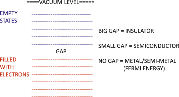
The explanation of grouping by resistivity was a triumph of electronic structure theory. If we take a box and fill it with electrons, we find that because of their quantum nature, these electrons are found in various discrete levels, as shown in Figure 2. These levels are separated because of the wave principles of quantum theory for confined particles, and each level can contain two electrons, spin-up and spin-down, due to the Pauli principle, so an even number of electrons can be added per atom or per cell until all possible levels are filled. If one adds a lattice of positive cores, there may be a gap in energy between the filled and empty states. If we try to create an electric current, for example by shining light or subjecting the electrons to an electric field, the electrons must jump the gap in order to conduct. In a metal or semimetal, there is no gap between the occupied and empty states, and an electron can easily conduct. The energy separating the occupied and the empty levels is called the Fermi energy, and the gap in a semiconductor is typically about 1 eV, while in an insulator, a typical gap is about 10 eV. If an electron moves from an occupied state to an empty state, then it can conduct, and if it moves to a high enough energy, it can escape from the crystal. That is the photoelectric effect, mentioned before in connection to Einstein’s Nobel Prize winning research.
Energy level diagrams for the electronic levels of the three main categories of solids, metals, semiconductors, and insulators.
Thus, differing resistivity can be explained in terms of the behavior of electronic states very near the fundamental gap or near the Fermi energy. However, explanations for most electronic and optical properties of solids require knowledge of the electronic structure over a wider energy range; we need to know the energies of all of the occupied levels and the empty levels. This information is obtained by studying optical properties of materials, because this enables us to observe how electrons move from occupied states into empty states.
Significant advancesReference Sommerfeld and Bethe5 in developing models of electron systems were made in the 1920s and 1930s, by assuming a box of electrons with a smeared out positive background to represent the positive cores of the lattice. These models were idealized and could not distinguish between different materials very easily. From the 1940s to the 1960s, researchers tried to perform calculationsReference Slater6,Reference Herring7 on real solids, but progress was very slow.
In contrast, theoretical progress using idealized models advanced at a rapid rate. In the 1950s, there were advances such as the theory of superconductivity by Bardeen, Cooper, and Schrieffer (BCS),Reference Bardeen, Cooper and Schrieffer8 which explained why some metals have infinite conductivity at a low temperature and why electrons can move around in a metallic ring forever, as long as the metal is kept cold. However, there was still no accurate detailed knowledge of the electronic band structure of Si (i.e., a determination of the dependence of the band energy as a function of momentum or wave vector).
The breakthrough came with a detailed study of optical data. In the mid-1960s, we were able to compute the electronic band structure of 14 semiconductors,Reference Cohen and Bergstresser9 because we were able to analyze the optical properties using the empirical pseudopotential method (EPM). Using this approach, by the 1970s, the physics of the optical structure of semiconductors was solved,Reference Cohen and Chelikowsky10 and in the 1980s, people extended the EPM to perform so-called ab initio calculations. The EPM required input to determine the atomic potential, and the three required parameters for each atomic potential were obtained from the optical data. The ab initio approach required no input information about the solid, only knowledge of the atoms and their atomic numbers to calculate the properties of the solid in a specific crystal structure. Since the 1990s, researchers have performed complex materials calculations for many properties of solids using these methods. In some cases, successful predictions of the existence of materials have been made before they were found in the laboratory.
Computational calculations
The main reasons for the breakthroughs were the development of new physical models, better computers, and improved measurements of optical spectra. Regarding the latter, one of the most important advances was in measuring not only the reflectivity of a solid as a function of energy but also the derivative of the reflectivity; this derivative contains much of the information about the detailed electronic structure of materials needed for use in the EPM. Figure 3 shows good agreement between theory and experiment for a derivative or modulated spectrum. The main discrepancies seen at low energies were later explained by exciton effects where excited electrons and holes interact. The electronic structure could thus be explained by the EPM using only the fitting three parameters for each type of atom in the solid.
Comparison of experiment and theoretical calculations for the derivative of reflectivity with respect to energy in Ge.

When interpreting experimental data and selecting among the associated theoretical models, it is understood that there are two popular standard models of a solid. The model I have discussed starts with a collection of atoms that is then combined into a solid and is regarded as a system of interacting atoms. The particles comprising the solid consist of stationary positive cores and negative valence electrons, which can move throughout the solid. The only interactions that need to be considered for these materials are the electromagnetic interactions—the Coulomb interactions. However, there are 1023 particles/cm3, which can lead to complicated effects. Figure 4 is an example of an interacting atoms model of a covalent semiconductor. The nuclei with the core electrons remain fixed while the valence electrons wander around. These negative valence electrons can situate themselves between the positive cores and form stable covalent bonds. This is not the correct structure for Si, but it illustrates the way Si is held together.
Schematic model of a covalent semiconductor showing the positions of atomic nuclei in black and the clouds of electrons forming bonds between them.
How do we calculate these structures? The way a valence electron interacts with a core must be understood. The electromagnetic interaction is a bit more complex than that for just two point charges of opposite sign. As shown in Figure 5, far from the core, the interaction potential causes a valence electron to be attracted toward the positive core, the standard Coulomb interaction. However, as the electron moves closer to the core, it is repelled due to the Pauli exclusion principle since only two electrons, spin up and spin down, can occupy any one state, and the core electrons have filled the states. If we take the Fourier transform of that simple potential and place it in a periodic lattice for systems, such as diamond or Si, or Ge or Sn, only three parameters are required to calculate the band structure.
Schematic model of a pseudopotential constructed from attractive and repulsive components.

For example, the band structure of Ge is shown in Figure 6, where the energy of various bands is shown as a function of wave vector. The optical properties can then be obtained by considering the transitions of electrons from occupied states below the gap region where there are no states to the empty states above the gap. Although band structure calculations of this kind using the EPM were performed many years ago, they are still among the most accurate and precise band structures available.
Electronic band structure of germanium in momentum space, where electrons can occupy states along each curve.

Another important piece of information obtained using the EPM is the probability of finding an electron in a specified position, and this is given by the square of the wave function. The charge density for Si is shown in Figure 7 for Si, illustrating the covalent bond.Reference Cohen and Chelikowsky10,Reference Walter and Cohen11 The plot shows the constant levels of density for electrons and how they form an egg-shaped blob of charge between the two cores. The covalent bond holds Si together. X-ray diffraction measurements show this feature was done after the theoretical predictions, which produced pictures of covalent bonds in a real solid for the first time.
Valence electronic charge density of silicon, showing increased density in the space between nuclei associated with a covalent bond. Reprinted with permission from Reference 10. © 1989 Springer.

The optical properties of semiconductors in the visible and ultraviolet originating from interband transitions were explained by an international experimental and theoretical collaboration in the 1960s and 1970s. The theoretical approach used to explain these properties was based on the EPM, a semiempirical approach that led to other empirical methods and even to ab initio approaches.Reference Hamann, Schluter and Chiang12–Reference Yin and Cohen15
As an example of a useful empirical approach derived from the EPM, it was shown that by examining optical properties of semiconductors and insulators, information can be uncovered about their structural properties. This was done to derive an equation for the bulk moduli of solids using only minimal input information about the solid.Reference Cohen16 The bulk modulus is the inverse of compressibility, and on first glance, it would not be expected that optical properties have a relation to how a solid responds to pressure. However, the average optical gap is related to the energy separation of the bonding and anti-bonding or conduction electrons, and it is known how this gap scales with iconicity and lattice constant. The result of a simple formula for the bulk modulus is
 $${\it B} = \left( {1971 − 220{\rm{X}}} \right)/{\it d}^{3.5} ,$$
where d is the bond length and X = 1 or X = 2 for compounds of Group III–V elements or of Group II–VI elements, respectively. This formula can be extended to other materials having different coordination. This simple formula requiring minimal input is in almost perfect agreement with experimental measurements on dozens of crystals. This is an example of how the use of the EPM, originally developed to explain optical properties, can provide information about structural and mechanical properties.
Another very important use of the EPM was to point to paths leading to a true ab initio approach where the calculation requires only information about the atoms composing the solid.Reference Hamann, Schluter and Chiang12–Reference Yin and Cohen15 The result was a method requiring only the atomic number to generate the pseudopotential and the atomic mass when the effects of lattice vibrations are involved. For determining structural phases, for example by examining different competing crystal structures at specific pressures, the input of candidate structures is also needed. In this case, the approach is to calculate the total energy of the system as a function of the structure, and then use the condition that the lowest energy structure would be the appropriate one at a given density. The total energy approach includes the energies from the cores interacting with each other, the cores interacting with the electrons, the kinetic energy of the electrons, the Coulomb interaction of the electrons, and the exchange and correlation interactions calculated from the density functional. From this information, the lattice constant can be calculated to better than 1% accuracy and the bulk modulus to less than 1%, as well as the electronic structure. The crystal structures, including high-pressure crystal structures, mechanical properties, vibrational properties, electrons interacting with lattices, and even superconducting properties can thus be calculated.
These calculations have other uses for insights into the general properties of materials. Figure 8 shows a comparison of the electronic density of diamond and Si.Reference Cohen17 For the diamond structure, by replacing silicon with carbon, the blob of charge that forms the covalent bond binding two silicon atoms together is replaced by a double-hump structure. This is extremely important; it can be associated with the fact that carbon forms structures important for biology and hence life itself. Silicon is said to be the basis of geology, and carbon is the basis of biology. The reason for this is that the silicon atom has p electrons in its core; p electrons have orbital angular momentum 1. These push the p valence electrons away because of the Pauli principle and puts them into the bond region. Carbon, which is in the first row of the periodic table, has no p electrons in its core, so they do not repel the p valence electrons. The result is that the valence electrons concentrate near their atomic positions and form a double-hump charge, implying that carbon can form multiple bonds to make important biological molecules unlike silicon. Based on this, it appears that all the science fiction articles and books about creating silicon biology are wrong. However, it is possible to make silicon devices and produce machines that compute and perhaps have artificial intelligence, but it is unlikely that silicon can play a similar role as carbon for biological applications. Carbon can also be used to make graphite and graphene, which are popular materials and the reason for this is the nature of the bond, as described previously.
The effect of silicon’s core p electrons is apparent in comparing the valence electronic charge density of solid carbon and silicon, where unlike silicon, the density of electrons in carbon has a double hump structure. Reprinted with permission from Reference Reference Cohen17. © 1973 AAAS.

Application to photovoltaics
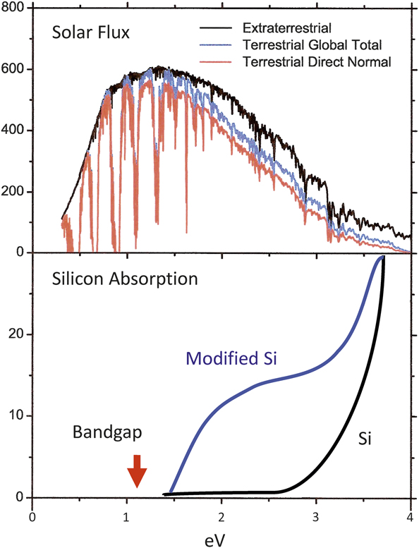
Our first example of calculations using the pseudopotential approach for applications concerns photovoltaics, an area that is receiving much attention, motivated by the goal to capture the energy from the sun and turn it into electricity to solve our energy problems. One approach, called bandgap engineering, is to find or design a semiconductor with a bandgap in the appropriate energy range so that the photons from sunlight are absorbed by the electrons to excite them over the gap, and in the process produce electricity. However, there is another approach other than tuning the bandgap to the solar spectrum that is probably more important, called wave-function engineering.Reference Cohen and Malone18 Silicon is the most popular photovoltaic, and when it is under pressure it can have a different structure, making it a better photovoltaic. However, it is not just a question of having a desirable bandgap; what is wanted eventually is a stronger absorber in the range of frequencies where sunlight is intense.
Although some high-pressure phases of Si were made before the theoretical studies in this area, the number greatly increased after many new structures of Si were predicted. It is rewarding to theorists that all the predicted structures have now been found experimentally. Si with the R8 structure is a good candidate for applications in this area and a useful example. As discussed previously, bandgap engineering requires the bandgap to be tailored, either by making new phases or via alloying or by doing something to the material to produce a gap in the right energy range. However, an important point is that not only should the gap be in the right range, the system must also absorb the sunlight in the desired energy range. This means a material with a desirable absorption coefficient as a function of energy is needed.
Figure 9 shows the solar spectrum and the absorption coefficients for two different structures of Si as a function of energy.Reference Cohen and Malone18 The bandgap in ordinary diamond structured Si is shown, together with the absorption coefficient, which is flat in the region where the sun spectrum peaks. However, if the Si is modified to a different structure like R8, the absorption coefficient increases even though the bandgap is almost the same as for diamond structured Si. Calculations of this kind are important applications of the methods described previously since they can provide information on the best path to useful photovoltaics.
Quantum calculations provided insights into the modification of silicon to better absorb light from the solar spectrum. Reprinted with permission from Reference Reference Cohen and Malone18. © 1973 AIP Publishing.
Application to nanotechnology
There is a great deal of research being discussed concerning nanostructures and nanotechnology, and it is fortunate that the theoretical methods previously discussed here are applicable for these systems. For example, we discussed the structure of diamond, where every carbon atom is surrounded by four other carbon atoms at a distance of 1.54 Å, but because of the particular bonding nature of carbon, it is also possible to make threefold-coordinated carbon, as found in graphite, where every carbon atom has three neighbors. This is the so-called sp 2 structure. In graphite, one-atom-thick layers (graphene) have short and, consequently, strong bonds. I noted earlier that the bulk modulus is proportional to 1/d 3.5, where d is the bond length, so graphene is stronger in this sense than diamond. However, the graphite in pencil lead, when it is pushed over paper, leaves layers of graphene that flake off. This is because the layers are separated by a wide distance, and the bonds between layers arise from the weak van der Waals interactions.
It is important to note that the properties of these systems can be studied and explained using the same computational approaches as those for bulk three-dimensional solids. Hence, theorists have gravitated toward this field focused on the interesting properties and variety of two-dimensional materials. For example, graphene layers can roll up to make carbon nanotubes, and theory can be used to explain the properties of these nanotubes.
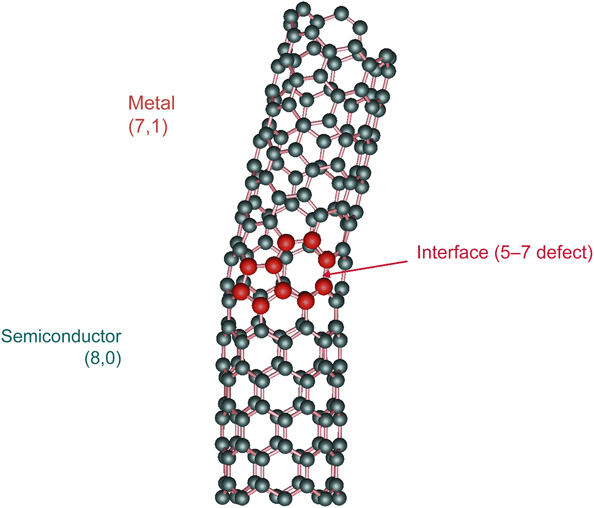
A sheet of graphene has carbon atoms arranged at the vertices of hexagons. If a graphene sheet is bent around so that eight hexagons are around the circumference, as shown in Figure 10, the tube behaves as a semiconductor. This tube is called an (8,0) nanotube, where the 8 refers to the number of hexagons along the circumference, and the zero means that we did not displace the hexagons along the direction parallel to the axis of the tube. However, if we roll a tube with seven hexagons, but move one hexagon up along the direction of the axis of the tube, that material is a (7,1) nanotube that behaves like a metal. If we join the two tubes together, this requires a defect, which instead of having two sixfold rings at the interface, we have a fivefold ring and a sevenfold ring. Hence, a semiconductor in contact with a metal has been constructed, and it behaves like a piece of Si in contact with a piece of Al. A device of this kind is a Schottky barrier. Using nanotubes, a Schottky barrier can be made on a very small scale, suggesting a new era in miniaturization of electronic devices.Reference Chico, Crespi, Benedict, Louie and Cohen19 This nanosystem was predicted theoretically and found experimentally.
Carbon nanotube [(8,0)/(7,1)] with a Schottky barrier resulting from the interface between two different types of nanotube structures. Reprinted with permission from Reference 19. © 1996 American Physical Society.
Another prediction is that boron nitride (BN) would form nanotubes,Reference Rubio, Corkill and Cohen20 and these were subsequently found experimentally.Reference Chopra, Luyken, Cherrey, Crespi, Cohen, Louie and Zettl21 In contrast to carbon nanotubes, which can behave either as semiconductors or metals, BN nanotubes are always semiconducting but with a wide bandgap of the order of about 5 eV. Although BN nanotubes are similar in structure to carbon nanotubes, they have some unusual and desirable electronic properties. For example, if we take a BN nanotube and dope it so that it is n-type, the charge travels through the center of the tube, acting like a pipe for electrons.
BN nanotubes have many applications. Yarn made of C nanotubes is black and hard to dye, while macroscopic materials made from BN nanotubes are white. In fact, sometimes a sheet of BN is referred to as white graphene. It is also possible to place buckyball, C60, molecules at the center of BN nanotubes and use them for a number of applications. BN nanotubes are more biofriendly than carbon nanotubes, making them promising materials for medical applications.Reference Cohen and Zettl22 The main problem associated with BN nanotubes has been the difficulty in making these tubes, so the supply could not meet demand, but there are new methods to make fabricating large amounts of BN nanotubes possible.
Quantum mechanics and philosophy and superconductors
Some concepts related to the philosophy of science must be introduced before discussing superconductivity. Fortunately, many modern science philosophers study quantum mechanics, and they are aware of what we are up against regarding knowledge and uncertainty. There have been some exciting discussions about how we interpret science related to the concepts of elementary excitations and emergence.
The model of a solid described earlier focused on the description of a solid as a system of strongly interacting atoms. A second model of a solid is often called the elementary excitations model. The first model involves building solids from collections of atoms, while the second model relies on the behavior of the solid when probed. The elementary excitations model is much simpler since one focuses on the results when a probe, such as light, temperature, or a magnetic field, is applied to a solid. The probe produces elementary excitations in the solid, and when the responses to the probe are examined, they are described in terms of the elementary excitations produced.
For example, the reflectivity of a material is a response function, which can be measured by shining light on its surface and comparing the incident and reflected light. A material can be heated, and the increase in its energy allows measurement of the heat capacity, which is the appropriate response function in this case. Once the response function is measured, the properties of this system can be explained in terms of the excitations, which are believed to be responsible for the observations.
A probe and response model of a solid can be thought of in terms of emergent behavior since certain excitations emerge. These can be viewed as fictitious particles or real particles. For instance, many scientists and engineers spend their entire careers researching and manipulating holes in semiconductors. A hole is simply the absence of one electron in a box of 1023 electrons per cm3. It is very difficult to take an electron out and then calculate the behavior of the system in terms of the other (1023 –1) electrons. It is much easier to trace the hole left behind. This approach is “real” in the sense that it explains the properties of a real material. If a solid is hit with a hammer, we excite sound waves characterized by the vibrations of atoms. However, since a wave and a particle can be understood as complementary, these waves can be thought of as particles. In this case, the particles are called phonons. Phonons and holes are both very important concepts in understanding the properties of materials.
The philosophy related to this aspect of science can be traced to the beginning of the 20th century. Among others, these ideas were discussed by Henri Bergson, a Frenchman who started his career as a mathematician and wrote an important thesis in mathematics.Reference Gerbson23 He decided that Einstein’s theory of relativity had problems and argued with him, but eventually conceded that Einstein was right, although some philosophers still discuss and question the correctness of Bergson’s concept of time compared to Einstein’s. In a sense, Bergson moved from mathematics research to physics research, then to philosophy, where he proposed that everything we know is through images associated with our senses. Bergson stated that this is the fundamental aspect of perceiving and explaining phenomena, and that is why people think of physical properties as emerging and these fictitious particles as emergent properties.
Today, researchers refer to emergence in theoretical physics. Cosmologists discuss the emergence of space time, and those in condensed-matter physicsReference Cohen, Chiao, Cohen, Leggett, Phillips and Harper24 consider emergent particles and try to explain properties of systems in terms of the type of particles that can emerge. There are also examples of emergent properties of materials. At low temperatures, some materials may become superconducting and have no resistance, and superconductivity is considered an emergent property. In magnetism, electron correlations cause a system to become magnetic below a specific temperature. There are quantum Hall effects, and recently there has been a considerable amount of research on topological insulators.
In 1911, Kammerlingh Onnes and his students in Leiden, Holland discovered superconductivity in mercury.Reference Onnes25 They were measuring the resistance of mercury down to very low temperatures, and the resistance became as close to zero as their instruments were able to measure. Today, we work very hard to predict the properties of superconductors. Most of the predictions have been based on the Bardeen–Cooper–Schrieffer (BCS) theory of superconductors, and they have been successful. At this time, some superconductors cannot be explained by the BCS theory, but there are many that are.
How do we apply the models described to predict the properties of superconductors? In the beginning, semi-empirical models and similar approaches to those used for calculating electronic band structures were used. Later, we were able to use ab initio models. Si can be used as an example. When pressure is applied to Si, it goes through many structural phase transitions. The phases that are semiconductors can be useful for photovoltaics, but some can be metallic. It was possible to predictReference Chang, Dacorogna, Cohen, Mignot, Chouteau and Martinez26 that under pressure, Si will transform to a simple hexagonal structural phase that is a metal, and at higher pressures to a hexagonal close-packed phase, which is also a metal.
We predicted the following: the existence of these materials and their stability, the lattice constants, the mechanical and electronic properties, the phonon or the vibrational properties, the electrons’ interactions with the phonons, the superconducting transition temperatures, and their temperature dependences. All that is required for these calculations as inputs are the atomic number, the atomic mass, and an estimate of the Coulomb interaction. These materials were discovered experimentally, and all the predicted properties were found to be correct. Both systems were found to be superconducting at the predicted temperatures. In some sense, Si at high pressures may be the best-understood superconductor.
Our standard models in condensed-matter theory are the interacting atoms model and the elementary excitations model described before. Science philosophers would say that the former is associated with reductionism since we know what particles are included and the forces, and that is all that is required. Those in the emergent properties camp would say that is not all you need, because things emerge. The point is often made that if one knew how to connect all the molecules in a human body, they would still not know if it were alive since life is an emergent property. Condensed-matter theorists use both approaches, and today they can explain and predict the ground state and excited state properties of many condensed-matter systems, but in the end, all decisions in physics are made by experiment. Theorists do not make the decisions; the experimentalists make the decisions on what is right, and they also have made all the major new discoveries until now.
Summary and conclusions
If I could learn von Hippel’s secret for a long life, then perhaps I could work on many of the areas being currently discussed. Because life is finite, the main question in fundamental and applied condensed-matter physics is this: “What kind of problems should we work on?” I do not have a definite answer, but I believe that energy production, storage, transmission, clean energy, better materials for all kinds of applications, and high-temperature superconductors are important. We are still trying to find room-temperature superconductors that allow trains to travel at the speed of airplanes. We want to interface with biology and improve our understanding of information technology, quantum computing, and correlated systems, and we want to predict new states of matter. These are just some important topics that might be important in the future, but I have to remind you that Yogi Berra said, “it’s tough making predictions, especially about the future.”
I have differentiated to some extent between basic and applied research. When a student asks me, “Should I concentrate on basic or applied science?” the answer is the same as the answer to “Is light a particle or a wave?” Yes. We need both. I also want to add a disclaimer since I have discussed mainly theoretical research and the results of theoretical studies, but Einstein warned that “the most valuable tool of the theoretical physicist is his wastebasket.” So, please be forewarned.
Acknowledgments
Over the past 50 years, the author has had the joy of working with outstanding students, postdoctoral researchers, and visitors from around the world and thinks it is wonderful to be able to work with people on the topics that he believes in. The author acknowledges support from NSF Grant No. DMR-10-1006184, and the theory program at the Lawrence Berkeley National Laboratory through the Office of Basic Science, US Department of Energy under Contract No. DE-AC02-05CH11231.
Marvin L. Cohen is a professor of physics at the University of California–Berkeley and senior faculty scientist at the Lawrence Berkeley National Laboratory, USA. In 2005, Cohen was president of the American Physical Society (APS). His research includes theoretical condensed-matter physics. He is a recipient of the National Medal of Science, the APS Oliver E. Buckley Prize for Solid State Physics, the APS Julius Edgar Lilienfeld Prize, the Foresight Institute Richard P. Feynman Prize in Nanotechnology, the Technology Pioneer Award from the World Economic Forum, the Berkeley Citation, and the Dickson Prize in Science along with other honors. He has honorary degrees from the University of Montreal, the Hong Kong University of Science and Technology, and the Weizmann Institute of Science. He has contributed more than 820 technical publications. Cohen is a Fellow of APS and the American Association for the Advancement of Science and a member of the National Academy of Sciences, the American Academy of Arts and Sciences, and the American Philosophical Society.


