

1. Introduction
Metalorganic chemical vapour deposition (MOCVD) and molecular beam epitaxy (MBE) are the most common methods for epitaxial growth of GaN films. Both techniques have their advantages. The MOCVD is a comparatively inexpensive method, because ultrahigh vacuum is not necessary. The MBE benefits from the clean environment and therefore low concentration of unwanted extrinsic defects, excellent control of the deposition parameters, and lower deposition temperatures which should lead to fewer thermally induced intrinsic defects. The plasma-enhanced molecular beam epitaxy (PEMBE) uses nitrogen radicals, produced in a nitrogen rf-plasma. Hydrogen, probably responsible for the passivation of dopants such as magnesium Reference Brandt, Johnson, Molnar, Singh and Moustakas[1], is thus avoidable during PEMBE growth in contrast to MBE using other nitrogen sources Reference Kingsley, Whitaker and Wee[2]. Despite these advantages, the best film quality has so far been achieved by the MOCVD method Reference Nakamura, Mukai and Senoh[3]. In this paper we discuss the PEMBE growth of GaN and emphasize some differences in MOCVD and PEMBE-grown GaN.
2. Experimental
The PEMBE GaN films are grown in a Tectra Mini MBE® chamber with a background pressure of 1 × 10⁻¹⁰ mbar . The gallium and aluminum sources are conventional hot lip and cold lip effusion cells, respectively. As nitrogen source, an Oxford Applied Research CARS25 radical beam source is used. In this source the molecular nitrogen is decomposed in a radio frequency (rf) plasma at 13.56 MHz. The activated nitogen is predominantly atomic nitrogen and has only a negligble fraction of ions Reference Hughes, Rowland, Johnson, Fujita, Cook, Schetzina, Ren and Edmond[4]. This is the main difference to the electron cyclotron resonance (ECR) plasma source, Reference Hughes, Rowland, Johnson, Fujita, Cook, Schetzina, Ren and Edmond[4] the other commonly used source for PEMBE growth of III-V nitrides. During the growth, the samples were rotated with 10 rpm to obtain uniform films over 2 inch (0001) sapphire wafers. Before deposition the substrates were pretreated by heating for 1 hour at 950 °C under N-radical flux. The deposition temperatures were varied from 650°C up to 825°C. The Ga flux onto the (0001) sapphire surface was 8 × 1014 cmȒ2s−1 as measured with a quartz microbalance. The pressure in the MBE chamber during deposition and pretreatment was 4 × 10⁻⁵ mbar. The inductively coupled rf power was 400W. Before the actual GaN growth, on several samples, AlN buffer layers of approximately 50 nm thickness were grown at 850 °C with an Al flux of 6 × 1013 cm−2s−1. To ensure that all of the Al metal on the wafer surface reacts to AlN, the N-radical flux was further maintained for 30 min.
The MOCVD samples were grown by low pressure MOCVD Reference Ambacher, Rieger, Ansmann, Angerer, Moustakas and Stutzmann[5], using ammonia and triethylgallium (TEG) as precursors for nitrogen and gallium at a temperature of 1020 °C on a 50 nm thick GaN buffer layer produced at 520 °C. The ammonia flux was 1.8 slm and hydrogen and nitrogen fluxes were 0.7 slm each. The flow rate of bubbled hydrogen was 10 sccm, yielding a flow rate of 1.8 μmol/min TEG in the reaction chamber. The resulting deposition rate was 1 μm/h. Typical concentrations of free carriers in 1 μm thick GaN films were 1x1017 cm−3 with a mobility of 100 cm2/Vs.
The XRD rocking curve measurements were performed with a single monochromatized two-circle diffractometer. The carrier concentration and mobility were characterized by Hall measurements, using the van der Pauw technique.
3. Results and discussion
For optimizing the film quality of MBE-GaN, several deposition parameters, such as Ga flux, buffer layer growth, and deposition temperature were varied. To prevent the formation of Ga droplets at low deposition temperatures, the Ga flux was set at 3 × 1014 cm−2s−1 (Figure 1) corresponding to a Ga effusion cell temperature of 950 °C.
Dependence of the deposition rate on substrate temperature and Ga flux.
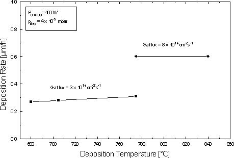
At a substrate temperature of 775°C, an increase in Ga flux to 8 × 1014 cm−2s−1 leads to a proportional increase in deposition rate. This fact, and a significant decrease of the growth rate by elevating the deposition temperature, are indicative of Ga-limited growth. An increase of the Ga flux for a given temperature also affects the electronic properties of the material. The Hall mobility remains at 35 cm2/Vs, but the carrier concentration decreased from 4 × 10¹⁸ for low flux to ne = 1 × 1017 cm−3 for elevated flux. This is evidence for reduced intrinsic defect density and therefore for improved stoichiometry. The structural quality does not change significantly, as shown by the XRD rocking curves with FWHM of 0.49° for both samples. The dependence of film quality on substrate temperature for GaN without an AlN buffer layer is shown in Figure 2. The increasing Hall mobility for constant charge carrier density, ne = 2 × 1017 cm−3, and the decrease in the XRD rocking curve FWHM is evidence for improvement, particularly in the structural properties of the epitaxial GaN.
The FWHM of the XRD rocking curve and the Hall mobility at 300K versus the substrate temperature for MBE grown samples. All GaN films have similar thickness (0.7 - 1.1 μm) and, for samples without a buffer layer, similar charge carrier densities (1 - 3 × 1017 cm−3).
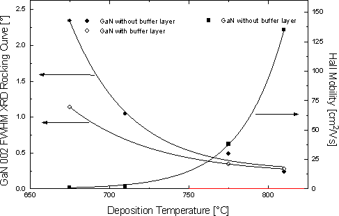
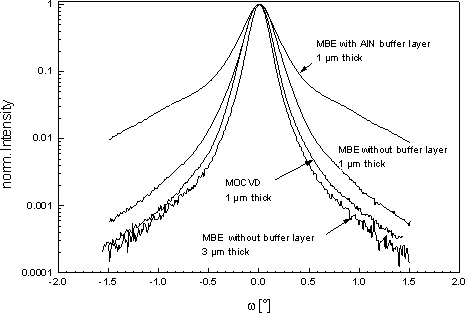
The improvement of film quality by the deposition of a thin GaN or AlN buffer layer is well documented for MOCVD Reference Yoshida, Misawa and Gonda[6] Reference Akasaki and Amano[7]. The growth of approximately 50 nm thick AlN buffer layers in MBE leads, especially at low deposition temperatures, to a reduced mosaicity of the GaN film, which is mainly responsible for the FWHM in the XRD rocking curves for symmetric reflections. Though no significant change in morphology occurred, nevertheless a drastic change in optical and electronic properties of the films was observed. The resistivity increased from about 103 Ω**cm for GaN films without a buffer layer to the order of 109 Ωcm for samples with an AlN buffer layer, thus preventing Hall measurements. Though the FWHM of the XRD rocking curve is not strongly affected by the buffer layer, a strikingly increased background due to diffuse scattering was measured for samples prepared at elevated deposition temperatures (Figure 3). This indicates that an AlN buffer layer has negligible influence in the growth direction [00.1], but strongly affects the formation of defects in other directions. PL measurements showed that the near-bandgap luminescence disappears for samples grown with an AlN buffer layer. This also points to the formation of deep defects that provide nonradiative recombination paths.
XRD rocking curves for MBE samples produced with the same parameters (Tdep = 810 °C, Ga flux = 8 × 1014 cm−2s−1), on a logarithmic scale. For comparison, a MOCVD sample with similar FWHM is shown.
In order to investigate the role of thickness on the film properties, a 3 μm thick sample was grown at 810°C with Ga flux of 8 × 1014cm−2s−1. Compared with a 1 μm thick film, the Hall mobility increased from 135 to 270 cm2/Vs for the same charge carrier density of 2 × 1017cm−3, and the FWHM of the XRD rocking curve decreased from 840 to 570 arcsec. This large influence is assumed to be due to decreasing defect density, particulary the reduction of grain boundaries, with increasing film thickness.
MOCVD samples with a similar rocking curve FWHM as the PEMBE films show less diffuse scattering, for the same sample thickness. This fact, and more directly a comparison of the morphology of PEMBE and MOCVD films (Figure 4), show that different growth mechanisms dominate. A three-dimensional growth for PEMBE films leads to epitaxial islands, responsible for a high surface roughness of about 30 nm and probably to abrupt interfaces between the crystallites. For the MOCVD samples, two-dimensional growth is achieved as indicated by smooth surfaces with a roughness of 5 nm, corresponding to 20 monolayers over 10 μm.
AFM surface image and depth profiles of PEMBE (left) and MOCVD (right) grown GaN with similar thickness and XRD rocking curve FWHM.

4. Conclusions
Several PEMBE deposition parameters were investigated for their influence on sample quality. An increase in Ga flux from 3 to 8 × 1014cm−2s−1 leads to a lower charge carrier density from ne = 4 × 10¹⁸ to 1 × 1017cm−3 respectively. In contrast to the growth of GaN by MOCVD, the use of AlN buffer layers did not improve the sample quality. The Hall mobility and the structural quality can be improved by the growth of thick samples. Comparing the morphology of PEMBE and MOCVD samples indicates that the mechanism is two-dimensional growth for MOCVD and three-dimensional growth for PEMBE, leading to a high concentration of inner interfaces. Nevertheless, GaN films with a Hall mobility μH = 270 cm2/Vs , charge carrier density ne = 2 × 1017cm−3 and XRD rocking curve FWHM of 570 arcsec are well suited for device fabrication by PEMBE.
This work was supported by the Bayerische Forschungsstiftung (FOROPTO II) and the Deutsche Forschungsgemeinschaft.


