Introduction
GaN based laser diodes have potential in a number of applications such as optical data storage, printing, full-color displays and chemical sensors. Additionally, medical applications of nitride based lasers include laser ablation of tissue (e.g. angioplasty), optical detection and selective destruction of malignant tumors, and autoflourescence imaging for the early detection of cancer. Major developments in recent years have led to lifetimes in excess of 10,000 hours demonstrating the viability of nitride laser diodes for commercial applications [Reference Nakamura, Senoh, Nagahama, Iwasa, Yamada, Matsushita, Kiyoku, Sugimoto, Kozaki, Umemeto, Sano and Chocho1].
Superlattices have been studied in the cladding for two reasons. First, it is difficult to grow thick AlGaN cladding layers needed for optical confinement due to cracking from lattice mismatch stresses during growth. AlGaN/GaN strained layer superlattices (SLSs) have been employed for strain relief of the cladding layer [Reference Ito, Hiramatsu, Amano and Akasaki2,Reference Nakamura, Senoh, Nagahama, Iwasa, Yamada, Matsushita, Kiyoku, Sugimoto, Kozaki, Umemeto, Sano and Chocho3]. Secondly, Mg-doped AlGaN/GaN superlattices have also shown an enhanced hole concentration. Kozodoy et al. show that a periodic oscillation of the valence band edge, such as superlattices employing alloys with different valence band edge positions, can help overcome the poor doping efficiency of a deep acceptor by forming a two-dimensional hole gas (2DHG) [Reference Kozodoy, Hansen, Mishra and DenBaars4]. This results from the ionization of acceptors when the band edge is far below the Fermi energy causing an accumulation of holes where the band edge is close to the Fermi level. Although the free carriers are separated into parallel sheets, their overall number may be much higher than in a simple bulk film. The average hole concentration of superlattice layers at room temperature increases by more than a factor of 10 over bulk films. This paper investigates the effect of vertical conduction of AlGaN/GaN superlattice cladding layers on InGaN laser diode structures.
Experimental Details
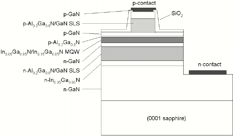
InGaN multi-quantum well laser diodes were grown by metalorganic chemical vapor deposition (MOCVD) in a two-flow horizontal reactor on c-plane sapphire substrates using both atmospheric and low pressure. The device structure shown in Figure 1 has an active region consisting of a 3 period In0.15Ga0.85N (40 Å)/In0.05Ga0.95N:Si (85Å) MQW with a 200 Å Al0.2Ga0.8N:Mg cap. The n- and p-type cladding regions surrounding the active region consisted of Al0.2Ga0.8N/GaN superlattices with a total thickness of 0.5 µm. The cladding regions were Si doped for the n-cladding and Mg doped for the p-cladding. The laser structures were grown with superlattice periods of 40 Å, 55 Å, 70 Å, 80 Å, 100 Å, 110 Å and 140 Å. The thickness of the AlGaN and GaN layers were the same yielding an average composition of 10% Al in the cladding. One structure was grown with a 0.5 µm thick bulk Al0.1Ga0.9N cladding layer for comparison purposes. A GaN:Mg layer was used for a contact layer and an In0.05Ga0.95N:Si layer is used beneath the lower n-type cladding as a compliance layer. The compressively strained InGaN compliance layer works to counteract the tensile strain of the n-cladding layer, thereby reducing the overall strain within the structure.
Layer structure for laser diodes with superlattice cladding layers.

Laser facets were formed by Cl2 reactive ion etching of 45 µm wide mesas of various lengths ranging from 400 µm to 1600 µm. P-contact stripes were formed on the mesas with widths ranging from 5 µm to 15 µm. The structure was etched around p-contact stripe through the p-cladding for index guiding as shown in Figure 1. The n- and p-contacts were formed by electron beam evaporation of Ti/Al/Ni/Au and Pd/Au respectively. Electrical testing was performed using pulses of 50 ns with a 1 kHz pulse repetition rate. The surface topography of the epitaxial structure was measured in tapping mode using a Digital Instruments Dimension 3000 scanning probe microscope. X-ray rocking curves of the GaN (102) ω peak were recorded using Ge(220)-monochromatic Cu-Kα radiation in triple axis mode. Specimens for transmission electron microscopy (TEM) were prepared by wedge polishing followed by standard Ar+ ion milling. Images were recorded on a JEOL 2000FX microscope operated at 200 kV.
Discussion
Structural Characterization
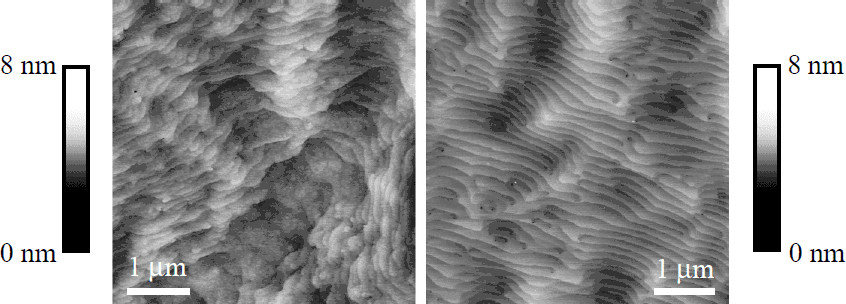
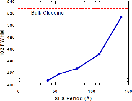
The structural quality of laser structures with superlattice cladding were superior compared to a laser structure with the bulk Al0.1Ga0.9N cladding as seen by atomic force microscopy (AFM) and off-axis x-ray diffraction (XRD). Figure 2 compares 5 × 5 µm AFM scans of a laser structure with bulk cladding layers and one with superlattices as the cladding. The surface morphology of the bulk cladding structure shows a poor step structure which appears to be a transition between two-dimensional step flow growth and layer by layer growth. The superlattice cladding sample has well defined steps formed by a step flow growth mode. The full width at half-maximum (FWHM) for the (102) GaN ω rocking curve is plotted versus strain layer superlattice period in Figure 3. The FWHM increases with increasing superlattice period and is greatest for the laser structure with bulk AlGaN cladding layers. Larger values of the (102) ω rocking curve FWHM indicate a higher presence of edge dislocations in the laser with bulk cladding [Reference Heying, Wu, Keller, Li, Kapolnek, Keller, DenBaars and Speck5].
5 × 5 µm AFM micrographs of laser structures with (a) bulk AlGaN cladding layers and (b) AlGaN/GaN superlattice cladding layers.
Full width at half-maximum (FWHM) for the (102) GaN ω rocking curve versus strain layer superlattice period. The FWHM value for the laser structure with bulk AlGaN cladding layers is indicated by the dotted line.
Device Characterization
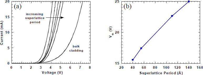
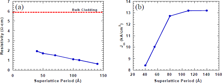
The effect of superlattice period is seen in the current-voltage (I-V) characteristics shown in Figure 4. The DC voltage of the devices increases with increased superlattice period and is dramatically higher for the bulk cladding. The threshold voltage of the laser diodes, which is the voltage measured at the threshold current, also increases with increasing superlattice period. Note that laser characteristics for the device with bulk claddings are not included since this sample did not lase. The voltage rise with increasing period can be explained by the lower probability for carriers to tunnel through the thicker AlGaN layers. The lateral resistivity of the superlattice layers decreases with increasing period as seen in the transmission line model (TLM) measurements of Figure 5a. Additionally, the threshold current density also increases with increasing superlattice period until it levels off for periods greater than 110 Å (Figure 5b). The increased threshold current density can be explained as an increase in surface recombination at the ridge as a result of the larger lateral conductivity of the larger period superlattice. Kozodoy et al. have shown that as the superlattice period increases, the spatially averaged hole concentration of AlGaN/GaN superlattices increases by more than ten times the value obtained for bulk AlGaN films [Reference Kozodoy, Hansen, Mishra and DenBaars4]. However, the increase in hole concentration associated with increasing superlattice period does not offset the enhanced resistance to vertical conduction through the p-type superlattice cladding observed for larger superlattice periods, thus higher voltages are observed.
(a) DC current-voltage (I-V) characteristics for laser diodes with 40, 55, 80, 110, and 140 Å period superlattice cladding layers and bulk cladding layers and (b) threshold voltage for laser diodes with varying superlattice period.
(a) Lateral resistivity of cladding layers for various superlattice periods as well as bulk. The bulk cladding is indicated with a dotted line. (b) Threshold current density for laser diodes with varying superlattice periods
Conclusion
InGaN MQW laser diodes with strained layer superlattices as cladding layers were shown to have superior structural and electrical properties compared to laser diodes with bulk AlGaN cladding layers. As the period of the strained layer superlattices is decreased, the threshold voltage is decreased. The current density also decreases with decreasing superlattice spacing. Since the vertical conduction does not improve with a larger overall hole concentration from the periodic oscillation of the valence band edge in the superlattice layers, the advantage of the superlattices as laser diode cladding layers is only for strain relief.
Acknowledgements
The authors would like to acknowledge the support of DARPA (R. Leheny), NSF, ONR (Max Yoder, Colin Wood, Yoon-Soo Park) and Hewlett Packard through the UC MICRO program (S.Y. Wang).