


Impact Statement
Optical elements such as microscopy phase masks, holography plates, and aberration compensation plates require well defined surface topographies with a high surface quality. Smooth topographies are also desired in a variety of biological applications such as anti-fouling and control of cell proliferation. Fabrication of smooth curved surfaces, particularly at the microscale, is a challenge for most fabrication techniques such as lithography, machining and three-dimensional printing.
In this work, we leverage dielectrophoresis, commonly used to manipulate micro-scale particles within liquids, to create nearly arbitrary deformations of a thin liquid film by applying a force distribution on its gas–liquid interface. Our results provide a practical methodology for the design of such systems, allowing to control the deformation shape and magnitude. Using photopolymers, the technique enables the fabrication of solid micro-scale objects with smooth (nanometer roughness) topographies.
1. Introduction
Dielectrophoresis (DEP) is a particular case of a force arising from the Maxwell stresses acting on dielectric materials containing permittivity gradients. The effect of DEP on particles has been studied extensively for over seven decades (Reference HughesHughes, 2000; Reference JonesJones, 1995; Reference PohlPohl, 1978). Significant advancement in microfabrication techniques in the early 1990s led to wider adoption of DEP, particularly in biological applications, as a method for control and manipulation of cells, viruses, proteins and DNA (Reference Chiou, Ohta and WuChiou, Ohta, & Wu, 2005; Reference Eberle, Höller, Müller, Suomalainen, Greber, Eghlidi and PoulikakosEberle et al., 2018; Reference HughesHughes, 2000; Reference Zhang, Shakiba, Chen, Zhang, Tian, Singh and WheelerZhang et al., 2018).
To date, only a few studies have examined the effect of DEP forces in geometries which are not particles, bubbles or droplets immersed in a liquid. Reference PellatPellat (Reference Pellat1894) was the first to study the effect of DEP on the rise of a dielectric liquid contained between two parallel electrodes. Extending Pellat's study, Reference JonesJones (Reference Jones2002), Reference Jones, Fowler, Chang and KimJones, Fowler, Chang, and Kim (Reference Jones, Fowler, Chang and Kim2003) and Reference Jones, Wang and YaoJones, Wang, and Yao (Reference Jones, Wang and Yao2004) investigated the influence of the liquid properties and the electric field frequency on the final height of the rising liquid, and used the term ‘liquid DEP’ (credited to Melcher (Reference JonesJones, 2002)) to describe problems associated with the motion of a liquid–air interface. Reference Jones, Gunji, Washizu and FeldmanJones, Gunji, Washizu, and Feldman (Reference Jones, Gunji, Washizu and Feldman2001) also studied the use of DEP forces for the generation and control of micro- and nano-droplets on solid surfaces.
The DEP actuation can also be leveraged for shaping the interface of a dielectric liquid film, as first demonstrated by Reference Brown, Wells, Newton and McHaleBrown, Wells, Newton, and McHale (Reference Brown, Wells, Newton and McHale2009), Reference Brown, Al-Shabib, Wells, McHale and NewtonBrown, Al-Shabib, Wells, McHale, and Newton (Reference Brown, Al-Shabib, Wells, McHale and Newton2010), Reference Brown, McHale and MottramBrown, McHale, and Mottram (Reference Brown, McHale and Mottram2011) and Reference Wells, Sampara, Kriezis, Fyson and BrownWells, Sampara, Kriezis, Fyson, and Brown (Reference Wells, Sampara, Kriezis, Fyson and Brown2011). In their original work, Brown et al. demonstrated the ability to deform a thin liquid film using DEP forces produced by an array of interdigitated electrodes. Using an electrode spacing of between 20 and 240 μm, they formed a fluidic diffraction grating with corresponding peak-to-peak spacings (Reference Brown, Wells, Newton and McHaleBrown et al., 2009). In follow-up work, they provided a detailed experimental study of the deformation scaling with the electric field magnitude, electrode spacing and film thickness (Reference Brown, Al-Shabib, Wells, McHale and NewtonBrown et al., 2010). Under the assumption of a periodic structure, and using a minimum energy approach, Brown et al. also provided an explicit analytical expression for the deformation (Reference Brown, McHale and MottramBrown et al., 2011). Wells et al. then showed that such structures could also be polymerized to yield solid optical components that no longer require the electric field to maintain their shape (Reference Wells, Sampara, Kriezis, Fyson and BrownWells et al., 2011). Their demonstration naturally raises the desire to create other, more complex, surface deformations. However, such generic deformations cannot be addressed by a periodic energy-balance approach.
In this work, we provide an alternative approach for the analysis for thin film deformations by DEP forces that does not rely on the assumption of a periodic structures. Instead of the energy approach, we utilize a force balance approach and model the spatial electric field created by pairs of electrodes patterned at the bottom of the fluidic chamber and calculate numerically the force distribution on the interface through Maxwell stresses. Coupling the DEP force with the Young–Laplace equation, we derive the governing equation describing the deformation of the interface. To validate the theory, we design an experimental set-up which allows spatial dielectrophoretic actuation, measurements of the microscale deformations and rapid curing of the deformed film into a solid object. Based on the insights from the characterization of the system, we demonstrate the ability to produce complex two-dimensional structures and provide guidelines for the design of such systems.
2. Concept and physical mechanism
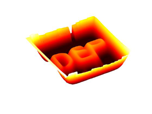
Figure 1 presents the concept of thin liquid deformation using dielectrophoretic forces. The system we consider consists of a fluidic chamber filled with a thin layer of dielectric liquid resting on top of a rigid substrate containing patterned electrodes. Aiming to achieve localized deformations, we use pairs of closely spaced electrode lines to define arbitrary paths along the chamber, as illustrated in figure 1(a). Upon setting an alternating current (AC) electric potential difference between the electrodes, a strong localized electric field is created. Figure 1(b) presents the electric field lines at the high frequency regime where the liquid acts like a perfect dielectric (Reference Castellanos, Ramos, González, Green and MorganCastellanos, Ramos, González, Green, & Morgan, 2003; Reference Morgan and GreenMorgan & Green, 2003). This electric field creates localized Maxwell stresses at the liquid–air interface (figure 1c), which in turn act to deform the interface (figure 1d). The permittivity difference in our system creates purely positive forces that push the interface upward; however, due to mass conservation, both positive and negative deformations are obtained. Figure 1(e) presents the deformation of a thin layer of silicone oil by DEP forces induced by an electrode pattern in the form of the word ‘DEP’.
Illustration of the concept of DEP-induced deformations. (a) Isometric view of the device used for inducing deformation, which consists of an open microfluidic chamber whose floor is patterned with pairs of electrodes leading to interface pads. The chamber is filled with a thin dielectric liquid film, forming a liquid–air interface. (b) A cut view of the chamber showing that upon actuation of the electrodes, a non-uniform electric field is established (potential map indicated in grey scale, electric field lines in blue). (c) The electric field induces Maxwell stresses on the interface with maxima in proximity to the electrode pairs. (d) The stresses deform the liquid–air interface, with the deformation extending far beyond the electrodes region. While the DEP force is non-negative everywhere, mass conservation dictates both positive and negative deformation. The green dashed lines in d indicate the corresponding region shown in b and c. (e) Image of a rectangular microfluidic chamber filled with silicone oil and patterned with the same electrode configuration presented in a, where actuation of the electrodes enables to reshape the interface creating complex and localized patterns such as writing the word ‘DEP’.

3. Results
3.1 Theoretical model
Consider a liquid resting on top of a rigid substrate patterned with conductive electrodes and open to the air from the top, as illustrated in figure 1(a) with a Cartesian coordinate system at the bottom where the x–y plane is parallel to the floor and the z coordinate pointing at the normal direction to the floor. The electric body force at any point in the system can be expressed as (Reference MelcherMelcher 1981)
 \begin{equation}\boldsymbol{f} = {\rho _E}\boldsymbol{E} - \frac{1}{2}{E^2}\boldsymbol{\nabla} \varepsilon + \frac{1}{2}\boldsymbol{\nabla} \left( {\rho \frac{{\partial \varepsilon }}{{\partial \rho }}{E^2}} \right),\end{equation}
where  ${\rho _E}$ is the free charge density, E is the electric field, $\varepsilon $ is the dielectric permittivity and $\rho $ is the fluid's density. Under the assumptions of a high frequency regime, i.e. $\omega \gg \sigma /\varepsilon $ (where $\omega $ is the electric field frequency and $\sigma $ is the fluid's conductivity), the liquid can be assumed to behave as a perfect dielectric, and the contribution of the free charges (first term in (3.1)) vanishes (Reference Castellanos, Ramos, González, Green and MorganCastellanos et al., 2003; Reference Ramos, Morgan, Green and CastellanosRamos, Morgan, Green, & Castellanos, 1998). Furthermore, if the liquid is assumed to have uniform permittivity, then the second term vanishes everywhere except at the interface where a discontinuity in permittivity exists. A convenient way to express the force distribution on the liquid–air interface is by considering the Maxwell stresses tensor, ${\boldsymbol{\mathsf{T}}_{ij}}$ (Reference MelcherMelcher, 1981) associated with (3.1),
 \begin{equation}{\boldsymbol{\mathsf{T}}_{ij}} = \varepsilon \left( {{E_i}{E_j} - \frac{1}{2}{\delta_{ij}}{E_k}{E_k}\left( {1 - \frac{\rho }{\varepsilon }\frac{{\partial \varepsilon }}{{\partial \rho }}} \right)} \right),\end{equation}
(where  ${\delta _{ij}}$ is the Kronecker delta) and evaluating its normal projection on either side of this interface (see detailed derivation in supplementary material section S1 available at https://doi.org/10.1017/flo.2021.13) provides the electrostatic force on the interface.
For convenience, we decompose the normal component of the electrostatic force on the interface into two terms representing the contribution of the permittivity discontinuity,  ${f_{DEP}}$, and of the electrostriction, ${f_{ES}}$:
 \begin{align}{f_{DEP}} &= \frac{1}{2}({\varepsilon _f}{|{{\boldsymbol{E}_{a,{\textbf{t}}}}} |^2} + {\varepsilon _a}E_{a,n}^2)\left( {1 - \frac{{{\varepsilon_a}}}{{{\varepsilon_f}}}} \right),\end{align}
 \begin{align}{f_{ES}} &= \frac{1}{2}\bigg[ {{{|{{\boldsymbol{E}_a}} |}^2}{\rho_a}{{\left( {\frac{{\partial \varepsilon }}{{\partial \rho }}} \right)}_a} - {{|{{\boldsymbol{E}_f}} |}^2}{\rho_f}{{\left( {\frac{{\partial \varepsilon }}{{\partial \rho }}} \right)}_f}} \bigg],\end{align}
where  ${E_{a,n}}$ and ${\boldsymbol{E}_{a,t}}$ are the normal and tangential electric field components at the air side of the interface, respectively. The subscripts a and f mark the air and the fluid domains. We note that both the normal and tangential components of the electric field contribute to the force distribution in the normal direction to the interface.
To calculate the shape of the liquid–air interface at steady state, we express the normal stress balance while accounting for surface tension and Maxwell stresses,
 \begin{equation}{P_f} - {P_a} + {f_{DEP}} + {f_{ES}} = \gamma \kappa ,\end{equation}
where  $\gamma $ and $\kappa $ are the surface tension and the mean curvature of the liquid–air interface, ${P_a}$ is the pressure in the air (which can be assumed constant) and ${P_f}$ is the fluid pressure distribution on the interface. To resolve the pressure everywhere in the liquid, we write the electrohydrostatic equation, $\boldsymbol{\nabla }p = \boldsymbol{f} - {\rho _f}\boldsymbol{g}$ (Reference StrattonStratton, 1941), which after integration yields
 \begin{equation}{p_f}(x,y,z) = {P_0} + {\rho _f}\bigg( {\frac{1}{2}{{\left( {\frac{{\partial \varepsilon }}{{\partial \rho }}} \right)}_f}{{|{\boldsymbol{E}(x,y,z)} |}^2} - gz} \bigg),\end{equation}
where g is the gravitational acceleration,  ${p_f}(x,y,z)$ is the pressure in the liquid and ${P_0}$ is a constant that can be determined from the boundary conditions (e.g. far from the electrodes, at the liquid–air interface, ${p_f}$ is equal to the atmospheric pressure). By substituting (3.4) and (3.6) into (3.5) we obtain
 \begin{equation}{P_0} + {\rho _f}\bigg( {\frac{1}{2}{{\left( {\frac{{\partial \varepsilon }}{{\partial \rho }}} \right)}_f}|\boldsymbol{E} |_f^2 - gh} \bigg) - {P_a} + {f_{DEP}} + \frac{1}{2}\bigg[ {{{|{{\boldsymbol{E}_a}} |}^2}{\rho_a}{{\left( {\frac{{\partial \varepsilon }}{{\partial \rho }}} \right)}_a} - {{|{{\boldsymbol{E}_f}} |}^2}{\rho_f}{{\left( {\frac{{\partial \varepsilon }}{{\partial \rho }}} \right)}_f}} \bigg] = \gamma \kappa ,\end{equation}
where h is the height of the liquid film. Importantly, the contribution of the electrostriction pressure in the fluid cancels out with the fluid's contribution to the electrostriction force distribution on the interface. Furthermore, using the Clausius–Mossotti law (Reference StrattonStratton, 1941),
 \begin{equation}\rho \frac{{\partial \varepsilon }}{{\partial \rho }} = \frac{{(\varepsilon - {\varepsilon _0})(\varepsilon + 2{\varepsilon _0})}}{{3{\varepsilon _0}}},\end{equation}
the electrostriction pressure in the air vanishes  $({\varepsilon _a} = {\varepsilon _0})$. The final equation governing the shape of the interface is thus
 \begin{equation}{f_{DEP}} - \gamma \kappa - \rho gh = {P_a} - {P_0}.\end{equation}
3.1.1 Two-dimensional model
While the system we consider in our experimental work is three-dimensional, significant insight into the DEP forces and the deformations of the liquid–air interface can be obtained through analysis of a two-dimensional system. Consider a two-dimensional fluidic chamber of length l and height  ${h_0}$ filled with a dielectric liquid of volume ${V_f}$ (per unit depth) creating a thin liquid film, as illustrated in figure 2. The floor of the chamber contains at its centre a pair of electrodes of width and gap ${l_e}$ and negligible thickness. The dielectric permittivities of the liquid and the air above it are ${\varepsilon _f}$ and ${\varepsilon _a}$, respectively, and the surface tension of the liquid–air interface is $\gamma $.
Two-dimensional illustration of the parallel electrode-pair configuration and the relevant physical parameters used in modelling the system. (a) A dielectric liquid of volume  ${V_f}$ is placed in a chamber of length l and height ${h_0}$, forming a thin film wetting the chamber's floor and walls. Two surface electrodes of width and gap ${l_e}$, are located at the centre of the chamber. The dielectric permittivities of the fluid and air above it are ${\varepsilon _f}$ and ${\varepsilon _a}$, respectively, and the surface tension of the fluid–air interface is $\gamma $. (b) A closer view on the electrode region. Since the dimensions of the electrodes are significantly smaller than the size of the chamber, we assume an approximately constant height for the liquid film for the purpose of electric field and force calculations.

The electric field and the deformation in the system are coupled. However, because the electric field decays rapidly away from the electrodes, we consider a simplified model in which the film thickness is uniform and equal to its value at the centre between the electrodes, as illustrated in figure 2(b). This approximation holds well for small deformations, and as evident by the experimental results, provides very good predictions also for large deformations.
We numerically solve the electrostatic Laplace equation in a domain containing the two fluids. Substituting the resulting electric field into equation (3.3) yields the force distribution on the interface. Figure 3(a) presents the DEP force distribution (stress) at the liquid–air interface for an electrode width of  ${l_e} = 120$, 180, 240 μm and a fixed film thickness of $h = 100\;{\rm \mu} \mathrm{m}$, showing that the maximum is achieved midway between the electrodes and decreases as the gap between the electrodes increases. This is expected, because a larger distance between the electrodes leads to a proportionally smaller electric field.
Two-dimensional finite-element simulation results showing the behaviour of the DEP force acting on the interface for electrode-pair configurations where the width of the electrodes is much smaller than the chamber length,  ${l_e} \ll l$. (a) The DEP force distribution on the interface along the chamber for three different electrode widths, with $h = {100}\;\mu m$, showing that the maximum achieved midway between the electrodes, decreases as the width of the electrodes increases. (b) A colour map showing the total force on the oil–air interface (integral over the DEP force distribution) as a function of ${l_e}$ and the film thickness h. The white dashed line indicates the electrode width that provides that maximum force for a given h. (c) As expected, for a fixed electrode width, the force decreases as the liquid thickness increases. We note the cross-over point indicating that the dependence of the force on the electrodes gap is inverted for sufficiently large film thicknesses. (d) The total DEP force as a function of the electrodes’ length for a fixed film thickness ( $h = {100}\;\mu m$), showing a non-monotonic dependence. The circles correspond to each of the cases in panel a. The simulations were performed using $l = {9}\;mm$, ${\varepsilon _f} = {2.5}{\varepsilon _0}$, ${\varepsilon _a} = {\varepsilon _0}$ and ${V_0} = {400}\;V$.

Observing figure 3(a), one may mistakenly conclude that the total force per unit depth on the interface,  ${F_{DEP}} = \int_{ - l/2}^{l/2} {{f_{DEP}}\,\textrm{d}\,x} $, also decreases with the increase in ${l_e}$. However, as shown in the figure 3(d), the total force is non-monotonic, and the cases ${l_e} = 180$, 240 μm provide a larger total force than ${l_e} = 120\;{\rm \mu} \mathrm{m}$, despite a lower maximum. Figure 3(b) presents the total force as a function of both ${l_e}$ and the film thickness h. Here, too, the non-monotonicity ${l_e}$ is evident across all h values, where for any film thickness, the maximum total force is obtained when setting ${l_e} = 1.85h$. As a result, while for $h > 0.54{l_e}$ the total force increases with ${l_e}$, for $h < 0.54{l_e}$ the dependence is inverted and the total force decreases with ${l_e}$. This behaviour can also be seen more explicitly in figure 3(c), presenting the total force as a function of h for different fixed ${l_e}$ values, equivalent to tracing figure 3(b) along vertical lines. The different decay rates of the force with h, result in the curves intersecting one another.
As presented in figure 3(a), the numerically obtained DEP force distributions strongly resemble a Gaussian. To facilitate an explicit expression for the deformation, we thus approximate  ${f_{DEP}}$ as a Gaussian of width (standard deviation) ${l_e}$, and an amplitude a set such that its total force matches ${F_{DEP}}$,
 \begin{equation}{f_{DEP}} = a\,\textrm{exp}\left[ { - {{\left( {\frac{x}{{{l_e}}}} \right)}^2}} \right],\quad a = \frac{{{F_{DEP}}}}{{{l_e}\sqrt \pi \,\textrm{erf}[l/2{l_e}]}}.\end{equation}
 Under the long-wave approximation (Reference LealLeal, 2007; Reference Oron, Davis and BankoffOron, Davis, & Bankoff, 1997), the interface curvature can be approximated as  ${\textrm{d}^2}h/\textrm{d}\,x^{2} = h^{\prime\prime}(x)$ and equation (3.9) can be written as
 \begin{equation}\gamma h^{\prime\prime} - \rho gh + {f_{DEP}} = {P_a} - {P_0}.\end{equation}
 We assume that the liquid is pinned at the edges of the chamber,  $h( - l/2) = h(l/2) = {h_0}$, providing two boundary conditions which are sufficient to solve equation (3.11) as a function of the constant pressure difference ${P_a} - {P_0}$. To then obtain the value of ${P_a} - {P_0}$, we require the total fluid volume to be conserved, $\int_{ - l/2}^{l/2} {h(x)\,\textrm{d}\,x} = {V_f}$. The complete solution, including the effect of gravity, is presented in the SI. For brevity, we here provide the more compact expression for the case of $g = 0$ and ${V_f} = {h_0}l$. It is also convenient to present the solution in terms of the deformation of the liquid–air interface relative to its initial state, $d = h - {h_0}$,
 \begin{align}d(\xi ) = A\left( {({ - 8{\textrm{e}^{ - {\xi^2}/{c^2}}} + 2{\textrm{e}^{ - 1/{c^2}}}(1 + 3{\xi^2})} )c + \sqrt \pi \left( {(2 + 6{\xi^2} - 3{c^2}({\xi^2} - 1))\,\textrm{erf}\left[ {\frac{1}{c}} \right] - 8\xi \,\textrm{erf}\left[ {\frac{\xi }{c}} \right]} \right)} \right),\end{align}
where  $\xi = 2x/l$ is the non-dimensional axial coordinate, $c = 2{l_e}/l$ is the non-dimensional electrode width and $A = {F_{DEP}}l/16\gamma \sqrt \pi \,\textrm{erf}[1/c]$.
In this work, we investigate only the case of  $c \ll 1$, corresponding to narrow electrodes compared with the length of the chamber. At this limit, the deformation magnitude scales with A, and is linear with the chamber's length, l and inversely proportional to the surface tension. Consistently with the assumption of $c \ll 1$, the spatial gradients of the deformation, $(\textrm{d}/\textrm{d}\,x)(d) = (\textrm{d}/\textrm{d}\xi )(d)(2/l)$, are independent of the chamber size l.
The solution for the deformation (3.12) is a function of the DEP force, which in turn depends on the fluid thickness. Therefore, to solve for the deformation for a given voltage we use an iterative solver. Using the DEP force calculated based on the initial fluid thickness, we obtain an initial solution for the deformation. Updating the DEP force using the obtained height of the interface above the electrodes yields a new solution for the deformation. We repeat the process until the relative change in interface height between iterations (evaluated at  $x = 0$) reduces below ${10^{ - 5}}$.
3.2 Experimental measurements
In figure 4(a) we present three-dimensional digital holographic measurements (Reference Cuche, Marquet and DepeursingeCuche, Marquet, & Depeursinge, 1999) of the deformation of an oil–air interface due to an electric field produced by a pair of parallel electrodes. The fluidic chamber has a width and length of  $l = 9\;\textrm{mm}$ and depth of approximately ${h_0} = 120\;{\rm \mu} \mathrm{m}$. The electrodes have a width and gap of ${l_e} = 120\;{\rm \mu} \mathrm{m}$ and span the entire length of the chamber. The dielectric fluid is a low-viscosity silicone oil with density $\rho = 913\;\textrm{kg}\;{\textrm{m}^{ - 3}}$, and surface tension $\gamma = 20\;\textrm{mN}\;{\textrm{m}^{ - 1}}$. We initially measure the oil–air interface in the absence of an electric field. This measurement is subtracted from all subsequent measurements, thus allowing us to isolate the deformation of the interface due to the electric field.
Experimental measurements and theoretical predictions of DEP-induced deformations using the parallel electrode-pair configuration. (a) A typical experimental result showing the three-dimensional shape of the deformations, resulting from actuation of a pair of electrodes positioned along the  $y$-axis. (b,c) The deformation along the x-axis at $y = {0}\ $ for different applied voltages and initial liquid volumes, respectively. The solid lines present the experimental results, and the dashed lines present the theoretical predictions, obtained from the two-dimensional model equation (3.11). The maximum deformation is achieved in the middle of the chamber, between the electrodes, and it increases as the applied voltage increases and decreases as the fluid volume (fluid height above the electrodes) increases. We use silicone oil with a dielectric permittivity of ${\varepsilon _f} = {2.5}{\varepsilon _0}$ and surface tension of $\gamma = {20}\;\textrm{mN}\;{\textrm{m}^{ - 1}}$, a square-shaped chamber with $l = {9}\;\textrm{mm}$, ${h_0} = {120}\;\mu m$, ${l_e} = {120}\;\mu m$ and an AC voltage with a frequency of 10 kHz.

In figures 4(b) and 4(c) we compare the experimental data with the theoretical predictions for the deformation along the x-axis, for different electrode widths and different fluid thicknesses. Increasing the applied voltage increases the electric field and results in larger deformations. Similarly, decreasing the initial liquid volume, which decreases the distance of the interface from the electrodes, also results in a higher electric field and larger deformations. Both effects, as well as the details of the spatial deformation, are captured by the model, in very good agreement with the experimental results. The results show that the use of the long-wave approximation is well justified even for the largest deformations, where the maximal slope of the interface is of the order of 100 μm over 1 mm.
Figure 5(a) presents the maximum deformation as a function of the applied voltage squared, showing good agreement between theory and experiments. At low voltages, the deformation magnitude follows well the voltage-squared dependence obtained from scaling of the DEP force. However, at higher voltages, the maximum deformations are lower than those suggested by the scaling. This is precisely because of the earlier mentioned coupling between the deformation and the electric force; at high voltages, the deformation becomes significant enough to affect (reduce) the electric field at the interface.
Comparison of experimental and theoretical results of the maximum deformation. (a) The maximal deformation as a function of the voltage squared for  ${l_e} = {120}\;\mu m$ and ${V_f} = {8}\;\mu l$. The black dashed line presents the theoretical prediction based on the one-dimensional model, the black crosses present the experimental results and the blue dashed line represents the linear scaling with $V_0^2$. When the deformation is small compared with the initial fluid thickness above the electrodes, the theoretical solution scales linearly with $V_0^2$, yet as the deformation becomes comparable to the initial film thickness, both theoretical and experimental results show a sub-linear behaviour with $V_0^2$, due to the inverse scaling of the DEP force with the film thickness. (b) Normalized maximum deformation as a function of the electrodes width for different voltages. The dashed lines present the theoretical predictions and the crosses represent the experimental results. For low voltages (e.g. ${V_0} = {100}\;\textrm{V}$, black line), the deformation decreases when the electrodes width ${l_e}$ increases, but above a certain value of ${V_0}$ the deformation increases as ${l_e}$ increases (e.g. ${V_0} = {800}\;\textrm{V}$, light grey line). This transition is associated with the cross-over in the total force ${F_{DEP}}$ observed in figure 3(c).

This coupling is also evident in figure 5(b) that presents the predicted and measured (normalized) maximum deformations as a function of  ${l_e}$, for different voltages. The dependence on ${l_e}$ is different for different voltages, to the extent that the trend is inverted between the lowest and highest voltages shown. This could be explained by the fact that higher voltages are associated with larger film thickness. For example, the case of 100 V yields deformations of several microns, whereas the 800 V case yields deformations of approximately 100 μm (both relative to an initial thickness of 35 μm). These film thickness values reside on opposite sides of the intersection region shown in figure 3(c), and thus the inverted dependence on ${l_e}$ is expected. This result elucidates that to achieve the maximum force, the electrodes width and gap ${l_e}$ should be chosen such that ${l_e} = 1.85h$ in accordance with figure 3(b), but where h is the post-deformation film thickness, rather than the initial one.
3.3 Fluid shaping
The electrode-pair configuration can serve as a basic unit for the creation of complex two-dimensional electrode structures. Figure 6(a1) presents experimental measurements of the oil–air interface topography resulting from the actuation of an electrode configuration tracing the letters ‘DEP’ on the surface (figure 6b1). The deformation clearly shows peaks along the electrode pairs, and the letters are clearly distinguishable. However, as also visible from the cross-section in figure 6(c1), the peaks are not well separated. During our experiments, we found that reducing the liquid volume can significantly increase the resolution and contrast of the deformation field. Figure 6(b2) presents the same electrode configuration and applied voltage, but with 2 μl instead of 4 μl of liquid, resulting in its accumulation primarily at the edges of the chamber and only minimally wetting of the floor. As a result, upon actuation of the voltage, the liquid is drawn from the edges of the chamber toward the electrodes. Since the proximity of the floor precludes significant negative deformations, as can be seen clearly from both figures 6(a2) and 6(c2), the resulting deformation shows a better separation of the peaks and consequently better-defined letters. The same conditions can be applied to other electrode configurations, as shown in figure 6.3. Here, the electrode pairs are patterned to form an outline of a Y-junction. Upon activation of the electric field, each electrode pair produces a vertical wall, forming the physical boundaries of a 60 μm deep and 1 mm wide Y-junction channel. As shown in supplementary movie S1, upon activation of the field, the deformation is rapidly formed, can be easily modulated in amplitude, turned on and off and quickly recovers from external forced disturbances.
Experimental results demonstrating the use of DEP-based deformation for the creation of complex structures. Each configuration is based on pairs of electrodes deposited on a desired pattern at the bottom of the fluidic chamber (b). Upon actuation of the electric field, the liquid deforms to obtain the desired shape corresponding to the electrode configuration. The dashed and solid black curves in the two-dimensional images present the shape of the interface before and after actuation, respectively, along the x-axis denoted by a white line in the three-dimensional figure. (1) Using  ${4}\;\mu l$ of liquid, the initial interface is curved and the displacement of the liquid from the periphery into the actuation region is distinctly visible in c1. Panel (a1) shows the resulting topography which reads ‘DEP’. (2) using only ${2}\;\mu l$ of liquid, the initial interface at the centre of the chamber is nearly flat, which results in accentuation of the deformations and improved resolution relative to the ${4}\;\mu l$ case, providing better contrast and readability. (3) Using ${2}\;\mu l$, we demonstrate the creation of a ${\sim} {1}\;\textrm{mm}$ wide, ${\sim} {60}\;\mu m$ deep microfluidic channel and a Y-junction.

Due to the nature of the liquid–air interfaces, the resulting surfaces of the produced structures are very smooth. Thus, replacing the silicone oil with a polymer opens the door to a fabrication of smooth solid structures. Figure 7(a) presents an example for a structure produced by deforming the interface of a photopolymer using the Y-junction electrode configuration; after the steady-state deformation is obtained, and while the electrodes are still active, we expose the film to 365 nm ultraviolet (UV) light for five minutes which leads to its solidification. Figure 7(b) presents the shape of the interface along a cross-section before polymerization (i.e. in liquid state) and following polymerization (i.e. in solid state), showing good agreement between the two. Figure 7(c) presents the surface quality of the solidified part. Fitting the measured data to a second-degree polynomial and subtracting it from the original curve provides an estimate for the surface roughness, which is of the order of 3.2 nm root mean square (r.m.s.) (figure 7d). The surface roughness may in fact be better, as this is the limitation of the digital holographic microscope, as shown by measurements of an atomically polished wafer (SI figure S5).
Experimental demonstration of the use of DEP-based deformation for the fabrication of smooth solid structures. (a) Image of a Y-junction fabricated by deformation and polymerization of a photopolymer. (b) Comparison of the cross-section along the chamber (indicated by the white dashed line in a) before and after solidification of the polymer. (c) Zoomed-in view of the surface at  $x = {0}$ (solid red curve) together with a second-order polynomial fit (black dashed curve). (d) The difference between the raw data and the fit provides an estimation of the surface quality, yielding an r.m.s. value of 3.2 nm.

4. Methods
We fabricated the devices using standard cleanroom microfabrication processes. We used a 4 in. borosilicate glass wafer (Borofloat33, Wafer Universe, Germany) as a substrate on which we patterned via lifting off a 6 nm consisting of 2 nm titanium, 2 nm platinum and 2 nm titanium. We used such a thin layer because it is semi-transparent in the visible spectrum and thus reduces the reflection of the holographic microscope's laser beam. We defined the fluidic chamber's walls by lithography processing of a 120–150 μm thick layer of SU8, created by spin coating of SU8-50 (Microchem AG, Germany) in two sequential steps.
We performed the experiments by placing at the centre of the chamber a few microlitres of low-viscosity silicone oil (cat. no. 317667, Sigma-Aldrich) of density  $\rho = 913\;\textrm{kg}\;{\textrm{m}^{ - 3}}$, refractive index $n = 1.403$ and surface tension $\gamma = 20\;\textrm{mN}\;{\textrm{m}^{ - 1}}$, measured using an optical tensiometer (Theta Flex, Biolin Scientific). We used a wave generator (TG5012A, AIM-TTI Instruments) connected to an amplifier (2210-CE, TREK) to deliver to the electrodes a 10 kHz sinusoidal AC electric potential at voltages (peak to peak) of up to 900 V.
The measurements of the DEP induced deformations were obtained using a digital holographic microscope (DHM-R1003, Lyncee Tec) through a 10× objective with a field of view of  $0.5 \times \textrm{0}\textrm{.5}\;\textrm{m}{\textrm{m}^2}$ (see detailed explanation in SI section 3). To obtain full coverage of the chamber area we used an automated stage (MS 2000, ASI) working in synchronization with the DHM camera. We dictated a constant movement of 407 μm and stitched the data to assemble the image of the entire oil–air interface.
For the polymerization experiments, we used a UV curable polymer (CPS 1050, Colorado Polymer Solutions) and activated the electrodes at a voltage of 400 V and frequency of 10 kHz. We solidified the polymer using two 12 W UV lamps with a wavelength of 365 nm for 5 min.
5. Discussion and conclusions
We presented a theoretical model and an experimental demonstration of a new and practical approach to create desired deformations of a liquid–fluid interface. Owing to their inherently smooth interfaces, the ability to shape liquid films holds great promise as a method to create and modulate optical components. We showed that the use of pairs of electrodes provides an effective method for creating desired deformations. Beyond their ability to form highly localized deformations, from a practical perspective, continuous parallel electrodes allow us to span significant portions of the working area using only a single connection at the edge of each electrode. Furthermore, we showed that the distance between the electrodes can be used to control the magnitude of deformation, allowing the deformation to vary along the electrode-pair path.
In the current work, we studied the steady-state deformation of the system. When using a polymer, the liquid film can be solidified to yield a permanent component that could be used outside of the DEP system. However, one potential advantage of a fluidic system, particularly in the context of adaptive optics (Reference Mishra, Murade, Carreel, Roghair, Oh, Manukyan and MugeleMishra et al., 2014; Reference Zohrabi, Cormack, Mccullough, Supekar, Gibson, Bright and GopinathZohrabi et al., 2017), is the ability to dynamically modulate it, transitioning from one configuration to another. Supplementary movie S2 demonstrates this concept using an array of parallel electrodes, where the actuation transitions dynamically between one set to another.
We focused on deformations of an oil–air interface, with a dielectric constant ratio of approximately 2.5. As indicated by equation (3.3), the force is proportional to this ratio, and thus much larger deformations can be expected when using liquids with a higher dielectric constant. A natural candidate would be water, with a relative permittivity that is ~30-fold greater than that of silicone oil. For sufficiently high frequencies, such a system can be considered to be governed by dielectric effects, yet for lower frequencies, one must consider conductivity effects that would not only alter the force on the interface (see SI section 1) but would also lead to additional effects such as Joule heating and internal flows which we did not consider in this work. Our theory can also be directly applied to liquid–liquid configurations, providing an opportunity to invert the permittivity ratio relative to the oil–air configuration, i.e. have the liquid with the lower permittivity be in contact with the electrodes. In such a case, the resulting force on the interface will be toward the electrodes rather than away from them. This may lead to larger deformations, due to the pulling force further increasing as the interface approaches the surface. Beyond a certain threshold, this is also expected to lead to instability and rupture of the film over the electrode's region.
Acknowledgments
I.G. acknowledges the support of ISEF and is grateful to the Azrieli Foundation for the award of an Azrieli Fellowship. E.B. acknowledges the support of the Adams Fellowship Program of the Israel Academy of Sciences and Humanities, the Yad Hanadiv (Rothschild) Foundation and the Zuckerman STEM Leadership Program.
Funding Statement
This project has received funding from the European Research Council under the European Union's Horizon 2020 Research and Innovation Programme, grant agreement 678734 (MetamorphChip).
Declaration of Interests
The authors declare no conflict of interest.
Author Contributions
I.G., A.G. and M.B. conceived the research; I.G. performed the experiments, led the development of the models and analysed the data; F.P fabricated the devices and contributed to the design of the experiments; E.B. and A.R. contributed to the model development; A.G. and M.B. directed the research; I.G., F.P., E.B., A.G. and M.B. wrote the paper.
Data Availability Statement
All data are available in the main text or in the supplementary information.
Ethical Standards
The research meets all ethical guidelines, including adherence to the legal requirements of the study country.
Supplementary Material and Movies
The supplementary material includes a supplementary information file with five sections and seven figures. We also provide two movies with this manuscript ad supplementary material. Supplementary material and movies are available at https://doi.org/10.1017/flo.2021.13.


 Open access