

 ) surfaces is presented, including results for In, Mg, Si, and H adsorbates. Emphasis is given to direct determination of surface structure employing experimental techniques such as scanning tunneling microscopy, electron diffraction, and Auger electron spectroscopy, and utilizing first principles computations of the total energy of various structural models. Different surface stoichiometries are studied experimentally by varying the surface preparation conditions (e.g. Ga-rich compared to N-rich), and the stoichiometry is included in the theory by performing calculations for various chemical potentials of the constituent atoms. Based on the work reviewed here, surface reconstructions for plasma-assisted molecular beam epitaxy growth of GaN (0001) and (000
1 Introduction
Gallium nitride and other III-nitrides have attracted considerable interest recently because of their applications for blue light-emitting diodes and lasers and for high frequency/high power transistors Reference Davis[1] Reference Akasaki and Amano[2] Reference Morkoc, Strite, Gao, Lin, Sverdlov and Burns[3] Reference Nakamura[4] Reference Johnson, Nurmikko and DenBaars[5] Reference Jain, Willander, Narayan and Van Overstraeten[6] Reference Doppalapudi, Moustakas and Nalwa[7]. These materials have several unique properties compared to the more conventional III-V semiconductors (GaAs, InP, etc.): they exist in both cubic (zincblende) and hexagonal (wurtzite) form, they are refractory, and some of the materials have large band gaps. The relatively small size of nitrogen, compared to Ga or In, in these compounds leads to a number of unique surface structures, which have been explored in several papers for the (001) growth surface of cubic GaN Reference Feuillet, Hamaguchi, Ohta, Hacke, Okumura and Yoshida[8] Reference Wassermeier, Yamada, Yang, Brandt, Behrend and Ploog[9] Reference Neugebauer, Zywietz, Scheffler, Northrup and Van de Walle[10]. For the technologically more relevant (0001) growth surface of hexagonal GaN, reports over the past 5 years have led to considerable understanding of its structure, for both bare and adsorbate covered surfaces. This article presents a review of these studies of the surface science of wurtzite GaN (0001) and (000
Common growth methods for GaN films include metal-organic vapor phase epitaxy (MOVPE) and molecular beam epitaxy (MBE). The latter can be performed using a plasma source for nitrogen (plasma-assisted MBE, or PAMBE) or using ammonia, which thermally decomposes on the growth surface (reactive MBE, or RMBE). The MBE technique by virtue of its ultra-high vacuum apparatus is more amenable to surface science studies, and most surface science work to date has been performed on samples grown by PAMBE. Such work constitutes the bulk of the material reviewed in this article. Reports of the surface science of GaN films grown by RMBE have also appeared Reference Held, Nowak, Ishaug, Seutter, Parkhomovsky, Dabiran, Cohen, Grzegory and Porowski[11] Reference Grandjean, Massies, Semond, Karpov and Talalaev[12] Reference Thamm, Brandt, Takemura, Trampert and Ploog[13], and one group has reported surface science results for MOVPE-grown material Reference Munkholm, Stephenson, Eastman, Thompson, Fini, Speck, Auciello, Fuoss and DenBaars[14]. Those works are discussed below in Section 3.5.
It is important to note that the (0001) and (000
Cross-sectional view of a wurtzite GaN crystal in a (11

Regarding nomenclature, we repeat here the recommendation made by Hellman et al., that the terms “Ga-terminated” or “N-terminated” should be avoided when referring to film or surface polarity. The actual termination of a film depends, of course, on the surface reconstruction and surface stoichiometry. These terms, Ga- or N-terminated, will however be occasionally used below when referring to the actual presence of a particular terminating layer of atoms on a surface.
In this article we review results for surface reconstructions of GaN (000
2 Bare Surfaces
2.1 N-polarity
2.1.1 Experiment
A number of early works have reported surface symmetries other than 1×1 for GaN surfaces, but the nature of these reconstructions was completely unknown Reference Hellman[15] Reference Sung, Ahn, Bykov, Rabalais, Koleske and Wickenden[20] Reference Ahn, Sung, Rabalais, Koleske and Wickenden[21] Reference Asif Khan, Kuznia, Olson and Kaplan[22] Reference Hughes, Rowland, Johnson, Fujita, Cook, Schetzina, Ren and Edmond[23] Reference Lin, Strite, Agarwal, Salvador, Zhou, Teraguchi, Rockett and Morkoc[24] Reference IWATA, ASAHI, YU, ASAMI, FUJITA, FUSHIDA and GONDA[25] Reference Hacke, Feuillet, Okumura and Yoshida[26] Reference Wong, Li, Dong, Deng, Lau, Tu, Hays, Bidnyk and Song[27] Reference Molnar, Singh and Moustakas[28] Reference Packard, Dow, Nicolaides, Doverspike and Kaplan[29]. The first paper to determine geometrical arrangements of reconstructions was the work of Smith et al. for the GaN(000
STM images of the GaN(000

The 1×1 reconstruction appears as a hexagonal array of corrugation maxima, with a lateral spacing equal to the c-plane lattice constant of GaN, 3.19 Å. The 3×3 is similar in appearance but displays an asymmetry within the unit cell as well as additional structure at lower biases. The asymmetry of the unit cell reflects the fact that each GaN bilayer has only three-fold symmetry. STM images confirm that this asymmetry reverses upon descending a single bilayer-high step on the surface. The 6×6 is made up of ring-shaped structures. Each ring has three-fold symmetry with lobes from three neighboring rings coming close together. This results in two different kinds of “‘holes” around the rings, one appearing deeper than the other. The c(6×12) reconstruction is qualitatively different in appearance from the previous three. Row-like structures are observed running parallel to 〈1
For determining structural models of the observed reconstructions, an important constraint is the number of Ga (and N) atoms involved in each structure. The observed surface reconstructions form when the surface is Ga-rich Reference Held, Nowak, Ishaug, Seutter, Parkhomovsky, Dabiran, Cohen, Grzegory and Porowski[11] Reference Smith, Feenstra, Greve, Neugebauer and Northrup[30]. Formation of the 3×3 reconstruction was found to require 0.145 ± 0.025 ML (ML = monolayer = 1.14 × 10¹⁵ atoms/cm2) more Ga than the 1×1 structure, corresponding to 1.3 ± 0.2 atoms per 3×3 unit cell. The 6×6 and c(6×12) require additional amounts of Ga, estimated to be 0.43 and 0.58 ML respectively relative to the 1×1 surface Reference Smith, Feenstra, Greve, Neugebauer and Northrup[31]. It is important to note that this “excess” Ga (over that required for the 1×1) is only weakly bound onto the surface. Above a temperature of about 200°C, the 3×3, 6×6, and c(6×12) all transform reversibly to a 1×1 arrangement believed to consist simply of the 1×1 Ga-terminated surface (described below) together with the excess Ga in a mobile, disordered (probably lattice gas) arrangement on the surface.
2.1.2 Theory
First principles total energy calculations of the relative stability of possible models of surface reconstructions can provide definitive determinations of the surface structure provided certain conditions are met. One requirement is that the system under consideration must be reasonably close to equilibrium. It is not obvious a priori that this requirement is satisfied in general by surface structures prepared by an MBE growth process. Nevertheless theorists have moved forward using a thermodynamic approach and there is now a widespread consensus that it is possible to obtain a reasonably complete mapping of the observed reconstructions by calculating the surface formation energies as a function of one or more of the atomic chemical potentials of the constituents. Prototypical examples of systems where this approach has achieved some success include the GaAs(001) and ZnSe(001) surfaces. The approach has also been successful in chemisorption systems such as Si(001)H. One of the objectives of work on GaN surfaces is to determine if the same theoretical approach will be successful for GaN and the other highly ionic wide-band-gap materials. At present the theoretical mapping for GaN is not complete: some of the observed reconstructions – such as the 6×6 and c(6×12) on the (000
For GaN one calculates the relative formation energies of surfaces as a function of the Ga and N chemical potentials (μGa and μN). The formation energy of a system comprised of Ga and N is defined as Ω = E − nGaμGa − nNμN. In this expression E is the total energy per supercell that is calculated for a structure containing the specified number of gallium and nitrogen atoms (nGa,nN). We assume equilibrium with bulk GaN: This implies the relation μGa + μN = μGaN(bulk), where μGaN(bulk) is the calculated energy per Ga-N pair for wurtzite GaN. This relation between the chemical potentials is used to eliminate either the gallium or nitrogen chemical potential as an independent variable and to write the formation energy as a function of a single chemical potential. The formation energy may then be written as Ω = Ega − (nGa − nN)(μGa − μGa(bulk)), where Ega is the formation energy corresponding to the Ga-rich limit, where by definition μGa = μGa(bulk). The relative energy difference between any two reconstructions may then be expressed as ΔΩ = ΔEga − (ΔnGa − ΔnN)(μGa − μGa(bulk)). The Ga chemical potential is bounded from above by μGa(bulk) and from below by μGa(bulk) − |ΔH| where ΔH is the heat of formation of GaN. We refer to the two endpoints of the allowed Ga chemical potential, μGa = μGa(bulk) and μGa = μGa(bulk) – |ΔH|, as the Ga-rich and N-rich limits. The thermodynamically allowed structures are those that have the lowest energy for some value of the Ga chemical potential within the allowed range Reference Qian, Martin and Chadi[32].
Total energy calculations for the (000
(a) The relative energies calculated for possible models of the GaN(0001) surface are shown as a function of the Ga chemical potential. (b) Relative energies for GaN(000

In N-rich conditions the most stable structure that has been obtained theoretically is the 2×2 Ga adatom model, with the adatom in an H3 site. The adatom forms three bonds to the N atoms in the layer below, and the length of these bonds is 1.98 Å. So far, a 2×2 structure has not been observed on the GaN(000
The Ga atoms in the 1×1 adlayer structure are each bonded to a single N atom and are separated from 6 other Ga atoms in the adlayer by a distance corresponding to a second-nearest-neighbor distance of bulk GaN, i.e. they are separated by about 3.2 Å. The relative stability of this type of structure is, at first sight, very surprising. To establish the plausibility of this structure a set of calculations was performed in order to determine how much of the binding energy of a Ga atom arises from intra-adlayer Ga-Ga interactions and how much arises from the Ga-N bonds Reference Smith, Feenstra, Greve, Shin, Skowronski, Neugebauer and Northrup[33]. Starting from a GaN(000
The other observed reconstruction of the GaN(000
Schematic view of structures determined for the (a) 1×1 Ga adlayer and (b) 3×3 adatom-on-adlayer reconstructions of GaN(000

The atop-registered 1×1 adlayer model is also energetically favorable in the case of In-terminated GaN(000
2.2 Ga-polarity
2.2.1 Experiment
Reconstructions of the GaN(0001) surface have been reported by Smith et al. Reference Smith, Feenstra, Greve, Shin, Skowronski, Neugebauer and Northrup[36]. Those Ga-polar films were grown by PAMBE, using homoepitaxy on MOVPE-grown Ga-polar GaN, or using Si-polar SiC(0001) substrates. Compared to the (000
The origin of the 2×2 surface reconstruction, in particular, is quite controversial. Smith et al. observe this structure only under N-rich conditions (it is not seen during growth, but it does appear when the Ga-flux is interrupted). They thus suggest that it arises from a 2×2 arrangement of N adatoms. In contrast, a number of groups have reported an intense 2×2 diffraction pattern during growth, as seen by reflection high energy electron diffraction (RHEED) Reference Hellman[15] Reference IWATA, ASAHI, YU, ASAMI, FUJITA, FUSHIDA and GONDA[25] Reference Hacke, Feuillet, Okumura and Yoshida[26] Reference Xue, Xue, Bakhtizin, Hasegawa, Tsong, Sakurai and Ohno[37]. This pattern has been attributed to a 2×2 arrangement of Ga adatoms Reference Hellman[15] Reference Xue, Xue, Bakhtizin, Hasegawa, Tsong, Sakurai and Ohno[37]. Following an exhaustive but unsuccessful search for this 2×2 structure seen during growth, utilizing different growth conditions and multiple N-sources, Smith et al. finally proposed that it might arise from some unintentional adsorbate in the growth systems, e.g. arsenic Reference Smith, Ramachandran, Feenstra, Greve, Ptak, Myers, Sarney, Salamanca-Riba, Shin and Skowronski[38]. Subsequent installation of an arsenic source into their MBE system led to an immediate detection of the intense 2×2 pattern (seen during growth), thus confirming its origin as being due to arsenic, as further discussed below in Section 3.3. Indeed, in several cases, the growth systems which reveal intense 2×2 patterns during PAMBE growth are known to have been previously used for GaAs growth Reference Xue, K. Xue, Kuwano, Sadowski, Kelly, Sakurai and Ohno[39] Reference Brandt[40]. It is important to note that the above comments regarding the identity of the commonly observed 2×2 pattern apply only to PAMBE growth; for RMBE, a 2×2 pattern with different characteristics than that seen during PAMBE has been reported Reference Thamm, Brandt, Takemura, Trampert and Ploog[13].
The 2×2 reconstruction observed by Smith et al. is prepared by nitriding the surface at a temperature of about 600°C. STM images reveal a disordered surface with small domains of 2×2, consistent with the fact that the 1/2-order lines seen in RHEED are not very sharp Reference Smith, Feenstra, Greve, Shin, Skowronski, Neugebauer and Northrup[36]. From total energy calculations for the Ga face, two different 2×2 structures are found to be energetically favorable within certain ranges of the Ga chemical potential as described below: a N-adatom (H3) 2×2 and a Ga-adatom (T4) 2×2 Reference Smith, Feenstra, Greve, Neugebauer and Northrup[30]. The fact the 2×2 seen by Smith et al. is formed by nitridation led them to suggest that it arises from N adatoms.
The 5×5 reconstruction is obtained by annealing the Ga-face at 750°C, depositing 1/2 ML of Ga, then re-annealing the surface to about 700°C Reference Smith, Feenstra, Greve, Shin, Skowronski, Neugebauer and Northrup[36]. The surface obtained by annealing at 750°C alone is found to be disordered, but the Ga deposition and re-annealing process stabilizes the surface via the 5×5 reconstruction. Compared to reconstructions found on the N-face, the Ga-face 5×5 is strongly bias-dependent, suggestive of a semiconducting surface. Shown in Figure 5 is a pair of STM images of the 5×5 reconstruction acquired at positive sample bias (empty states) in (a), and negative sample bias (filled states) in (b), from nearby surface locations. At positive sample bias, the unit cells of the 5×5 can be readily identified by the dark trenches traversing the image in all three of the 〈11
Simultaneously-acquired dual bias images of the 5×5 reconstruction. Sample biases are +1.0 V and −1.0 V with gray scale ranges of 0.5 Å and 0.9 Å for (a) and (b), respectively. (From Reference Smith, Feenstra, Greve, Shin, Skowronski, Neugebauer and Northrup[36]).

Detailed analysis of the voltage-dependent images of the 5×5 leads to the model shown in Figure 6. The topographic maxima seen in the images are interpreted in terms of N and Ga adatoms, residing on T4 and H3 sites respectively, together with some residual dangling bonds in the unit cell. A complete theoretical description of this surface is lacking at present, although some results are available for the relative stability of Ga and N adatoms on the surface as discussed in Section 2.2.2 below.
Structural model for the 5×5 reconstruction. Ga-adatoms in T4 sites and N-adatoms in H3 sites are shown by large black and large grey circles respectively. The small open circles in the diagram represent the Ga rest atoms in the 2nd layer. In the locations where the small open circles are missing, Ga vacancies occur. The N atoms in the 3rd layer are not shown. The light grey circle labelled DB (dangling bond) is a particular Ga rest atom site. In an alternative model, this site could conceivably contain another adatom in a nearby T4 or H3 site. (From Reference Smith, Feenstra, Greve, Shin, Skowronski, Neugebauer and Northrup[36]).

The 6×4 is formed by depositing 1/2 ML of Ga onto the 5×5 and then briefly heating the surface up to 700°C. Ga deposition alone will not produce the 6×4, suggesting that the formation of the 6×4 must involve extensive rearrangement of surface atoms. Surfaces showing clear 6×4 RHEED patterns obtained in this manner, however, are also found to contain large domains of 5×5, as shown in Figure 7. Seen there are STM image of both the 5×5 and 6×4 regions, at both positive sample bias and negative sample bias. As with the 5×5, the row-like 6×4 structure shows a strong bias-dependence, again suggesting a semiconducting surface. At positive sample bias, each row is clearly defined by a line of bright features spaced 4×a (a = 3.19 Å) apart along the [11
Dual bias images of the 5×5 and 6×4 reconstructions. The average height difference between the two reconstructions is 0.3 Å for empty states (+1.0 V sample voltage) shown in (a) and 0.4 Å for filled states (−1.0 V sample voltage) shown in (b), with the 5×5 being higher in each case. In both images the total gray scale range is about 1.3 Å. (From Reference Smith, Feenstra, Greve, Shin, Skowronski, Neugebauer and Northrup[36]).

As seen in Figure 7 the 6×4 appears topographically lower, on the average, than the 5×5. This is counter-intuitive since the 6×4 is formed by adding Ga to the 5×5. One possible explanation is that the height difference is electronic in nature. However, this seems insufficient to explain the difference since the 5×5 is higher than the 6×4 at both positive sample bias (by 0.3 Å) and negative sample bias (by 0.4 Å). A second possibility is based on the observation that 6×4 surfaces not only contain 5×5 but also “1×1” Reference Smith, Feenstra, Greve, Shin, Skowronski, Neugebauer and Northrup[36]. This latter structure as described below is known to contain much more Ga compared to the other reconstructions, as measured by Auger electron spectroscopy (AES). The fact that all three reconstructions are found together suggests that the 5×5 and 6×4 may not be very different from each other in terms of energy, and possibly also Ga coverage. The “1×1”, on the other hand, appears to be energetically much more favorable, effectively acting as a Ga “sink”. In any case, it is hard to imagine that the 6×4 could contain less Ga than the 5×5. The additional Ga in the 6×4 could form a structural arrangement allowing a denser packing of Ga compared to the 5×5. The observed height difference might then be explained by a combination of both structural and electronic effects.
As reported by Smith et al. Reference Smith, Feenstra, Greve, Shin, Skowronski, Neugebauer and Northrup[33] the most stable structure at high Ga coverage is one which displays a diffraction pattern dominated by 1×1 spots, so that this structure is known as pseudo-1×1 or “1×1”. The structure can be formed in several ways, one of which is by depositing about 1 ML of Ga onto the 6×4, followed by a rapid anneal to 700°C. Another way to form the “1×1” is to terminate the growth of GaN under slightly Ga-rich growth conditions. As the sample cools, the entire surface can become “1×1” although 5×5 and 6×4 may also be observed, depending on the precise amount of Ga present on the surface. The diffraction patterns of this surface show mainly 1×1 streaks (in RHEED) or spots (in low-energy electron diffraction, LEED), but includes sidebands or satellite spots in these patterns as described below. Hence this structure is referred to as “1×1”, using the quotation marks to indicate that the symmetry is not truly 1×1. During growth, this Ga-rich surface shows only 1x streaks, as illustrated in Figure 8(a). However, as the surface is cooled down to 〈350°C, distinct sidebands appear on the high wavevector sides of the first-order streaks along the [11
1×1 RHEED pattern for GaN(0001) during growth, (a), and after cooling to below 350°C, (b), where it converts to a 1+1/6 pattern. The 1+1/6 LEED pattern (Einc =100 eV) is shown in (c). For most “1×1” surfaces (see text), a 1+1/12 pattern is observed below 200°C, as shown in (d) (Einc =40 eV). LEED in vicinity of (0,1) spot (Einc =40 eV) at various temperatures: (e) RT-100°C, (f) 100-150°C, (g) 150-200°C, and (h) above 350°C. (From Reference Smith, Feenstra, Greve, Shin, Skowronski, Neugebauer and Northrup[33]).

The temperature dependence of the 1×1 surface is illustrated in Figs. 8(e–h), focusing on the vicinity of the integral order (0,1) spot. Between room temperature and about 100°C, as seen in Figure 8(e), a modulated ring of intensity with radius 0.08 k 1 is observed around the (0,1) spot with modulation at 60° intervals. This ring has greater intensity on the high wavevector side of the spot. As the temperature is increased to about 150°C, the ring modulation decreases slightly [Figure 8(f)]. As the surface temperature increases further to around 200°C, the ring modulation decreases further [Figure 8(g)]. It is also seen that the radius of the ring appears to have decreased slightly to about 0.07 k 1. As the temperature is raised past 200°C, the pattern converts to 1+ 1/6 (although not observed in this particular LEED experiment, the conversion from 1+ 1/12 to 1+ 1/6 in this temperature range has been observed consistently in RHEED experiments). Above 350°C, one sees only the integral order LEED spot [Figure 8(h)]. This sequence of phase transitions is reversible. Thus we find that the ring modulation decreases with increasing temperature. At the same time, the ring radius decreases slightly from 0.08 k 1 to 0.07 k 1 with increasing temperature until about 200°C, at which point it increases by a discrete amount to 0.16 k 1.
The “1×1” diffraction patterns described above are typical of a incommensurate surface structure. The modulated ring structure and its temperature dependence indicate that this incommensurate structure possesses considerable dynamic, fluid-like character, even at room temperature. Thus, it was inferred that the “1×1” surface at room temperature is best characterized by a discommensuration-fluid phase Reference Smith, Feenstra, Greve, Shin, Skowronski, Neugebauer and Northrup[33], similar to that seen for Au(111) and Pt(111) at elevated temperatures Reference Abernathy, Gibbs, Gruebel, Huang, Mochrie, Sandy and Zehner[41]. Since the melting point of bulk Ga (29.8°C) is very near room temperature, such a structural phase for this Ga-rich surface is most reasonable. STM image for this surface generally do not display any atomic corrugation. Rather, the “1×1” regions appear quite featureless. Sometimes corrugation is seen, and in those cases it has precise 1×1 spacing (rather than some much longer corrugation, as would be expected from the diffraction results) Reference Smith, Feenstra, Greve, Shin, Skowronski, Neugebauer and Northrup[33]. This apparent discrepancy between the STM and diffraction results was resolved by postulating a model in which the surface contains two monolayers of excess Ga in an incommensurate arrangement, with this Ga existing in the mobile, fluid-like state at room temperature. Thus, the STM images reflect the time averaged position of the Ga atoms, which reflects the underlying 1×1 structure of the GaN bilayer below the excess Ga. In one exceptional case of STM imaging on the (000
STM images acquired at room temperature for a surface containing a mixture of “1×1”, 5×5, and 6×4 domains reveal a height difference of “1×1” islands relative to surrounding 6×4 and 5×5 regions of about 2.1 Å. Electronic effects can of course influence this height, but typically by only a few tenths of an Å. As discussed above, the 5×5 and 6×4 regions are believed to contain adatoms with height (from theory Reference Smith, Feenstra, Greve, Shin, Skowronski, Neugebauer and Northrup[36]) of about 1.7 Å above the Ga atoms in the outermost GaN bilayer. Thus, the thickness of the “1×1” Ga layer is estimated to be about 3.8 Å, corresponding to about 1.8 ML. This estimate suggests that the “1×1” reconstruction contains around 2 ML of excess Ga. Similarly, AES measurements indicate that the “1×1” surface contains 2-3 additional ML of Ga above the outermost GaN bilayer Reference Smith, Feenstra, Greve, Shin, Skowronski, Neugebauer and Northrup[33]. Recent results of RHEED studies for Ga on GaN(0001) and AlN(0001) also yield a value for the stable coverage of Ga on those surfaces under Ga-rich conditions of about 2 ML Reference Mula, Adelmann, Moehl, Oullier and Daudin[43].
The above diffraction results for the “1×1” structure have recently also been clearly observed using low energy electron microscopy (LEEM) Reference Pavlovska and Bauer[44] Reference Pavlovska and Bauer[45]. Transitions between the 1+ 1/6 and 1+ 1/12 structures were found to occur reversibly, as a function of temperature and Ga coverage. The state of the surface was monitored in real-time during growth, and it was found, in agreement with prior work, that the presence of the Ga bilayer associated with the “1×1” structure stabilizes the (0001) surface and gives rise to the flat morphology. Under Ga-poor conditions the bilayer disappeared and the morphology became rough and microfaceted (for more discussion of this phenomena see Section 4). So long as the microfaceting was not too severe, it could be eliminated by restoring the Ga double layer during growth.
Based on the data of Smith et al. a model was proposed in which the “1×1” surface consists of a double layer of Ga atoms, with 7 unit cell of the Ga atoms residing on 6 unit cells of the GaN Reference Smith, Feenstra, Greve, Shin, Skowronski, Neugebauer and Northrup[33]. The resulting spacing between the Ga atoms in the double layer is then close to what is ideally obtained in bulk Ga, and in energy minimization calculations for free-standing Ga bilayers. This laterally contracted bilayer model is illustrated in Figure 9. Although a complete theoretical description of such a model is currently not possible (because a 6×6 unit cell would be required), a simplified version of the model with √3×√3 symmetry has been shown to be energetically favorable under Ga-rich conditions Reference Northrup, Neugebauer, Feenstra and Smith[46], as further discussed in the following Section.
Side view of a possible structural model for the “1×1” surface (at a given instant in time) consisting of 2.7 ML of Ga sitting on top of the Ga-terminated bilayer. The empty circles represent the various possible positions of first-layer Ga atoms plotted with respect to each of several GaN unit cells, illustrate the time-averaged height of the first layer Ga atoms and thus the 1×1 contour which the STM tip will follow. At a given instant in time, however, this incommensurate structure will manifest itself in diffraction as satellites surrounding the integral order peaks. (From Reference Smith, Feenstra, Greve, Shin, Skowronski, Neugebauer and Northrup[33]).

2.2.2 Theory
Let us now turn to theoretical results for structures on the (0001) surface. A large number of possible structures were considered theoretically by Smith et al. Reference Smith, Feenstra, Greve, Neugebauer and Northrup[30] and many could be ruled out on the grounds that they are thermodynamically unstable. A simple 1×1 Ga terminated N-Ga bilayer model (i.e. the “ideal” surface) can certainly be excluded. In this structure the Ga atoms at the surface are threefold coordinated – each Ga is bonded to three N atoms and there is one Ga dangling bond per atom. The total energy calculations shown in Figure 3(a) indicate that there is no region of the chemical potential space for which this structure is stable. Adding one monolayer of Ga to this 1×1 Ga-terminated bilayer leads to the 1×1 Ga adlayer structures. Several possible adlayer registries (H3, T4, atop) were considered but in no case was a thermodynamically stable structure found. It is interesting to note that the surface energies of these Ga adlayer structures are rather insensitive to the registry. This has implications for the existence of stable incommensurate adlayer structures discussed below. After an extensive search it was ultimately surmised that there exists no stable structure having a true 1×1 symmetry for the clean GaN(0001) surface Reference Smith, Feenstra, Greve, Neugebauer and Northrup[30]. It was also determined that the 2×2 Ga vacancy model is not stable on the (0001) surface. This structure is slightly higher in energy than the N-H3 adatom model. The instability of the Ga vacancy model for GaN(0001) is interesting in view of the fact that a 2×2 Ga vacancy structure is known to exist on the GaAs(111) surface Reference Tong, Xu and Mei[47] Reference Chadi[48].
On the basis of the results shown in Figure 3(a) only the 2×2 N adatom and the 2×2 Ga adatom survive as potential candidates as thermodynamically stable structures on the GaN(0001) surface. The question then is which, if either, of these two models corresponds to the 2×2 structure that is observed. Given that the 2×2 structure seen in experiment is the least Ga-rich of all the observed reconstructions, and that it is often observed following an interruption in the Ga flux, it seems more likely that the observed 2×2 structure arises from N rather than Ga adatoms.
Of the two possible adsorption sites for the N adatom, the H3 site is preferred over the T4 site in the calculations by 0.7 eV/(2×2) cell Reference Smith, Feenstra, Greve, Shin, Skowronski, Neugebauer and Northrup[36]. A qualitatively similar result has been predicted for N adatom structures on the AlN(0001) surface, where the preference for the H3 site is 3.3 eV/(2×2) cell Reference Northrup, Di Felice and Neugebauer[49]. As yet there exist no experimental determinations of the site preference of N adatoms on either GaN or AlN surfaces. In the case of the 2×2 Ga adatom model a slight preference for the T4 site is predicted: the energy difference is about 0.12 eV/(2×2) cell Reference Smith, Feenstra, Greve, Shin, Skowronski, Neugebauer and Northrup[36]. The different site preference exhibited by the N and Ga adatoms on the (0001) surface is related to their very different ionicities.
Concerning the Ga-adatom 2×2, it appears that it has a higher energy than the 5×5 and “1×1” structures (described below), so that the Ga-adatom 2×2 is not actually energetically allowed (even though it is employed in many theoretical computations since it is a relatively simple structure).
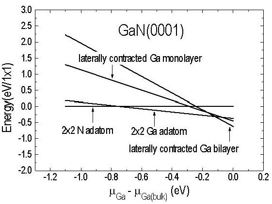
Let us now consider the pseudo-1×1 structure that is observed under very Ga-rich conditions. Although the STM corrugation pattern exhibits 1×1 symmetry the electron diffraction patterns obtained at temperatures less than 350°C reveal, in addition to the 1×1 spots, additional diffraction intensity in satellite spots Reference Smith, Feenstra, Greve, Shin, Skowronski, Neugebauer and Northrup[33]. These diffraction patterns indicate that the lattice vectors of the unit cell are in fact larger than those corresponding to a 1×1 cell, and furthermore it is found from Auger spectroscopy that the structure contains 2-3 ML of Ga in excess of that expected for a bulk terminated GaN surface. To explain these observations a laterally contracted Ga bilayer model has been proposed Reference Northrup, Neugebauer, Feenstra and Smith[46], shown in Figure 10. In this model the atoms in layer 1 are located in atop sites and are separated by a = 3.19 Å. However, the atoms in the top layer (layer 0) are contracted. This lateral contraction of the top layer is proposed because calculations have shown that a lateral contraction of such an adlayer – so that the Ga-Ga separation is reduced from 3.19 to 2.75 Å – is energetically favorable. This reduction in the spacing results in an increased density of atoms in the adlayer and therefore provides a natural explanation of the Auger data, which is suggestive of an increased Ga content (greater than 2 ML) on the surface. Total energy calculations for such an adlayer were performed using a √3 × √3 unit cell. Different registries of layer 0 were considered, as shown in Figure 10, but the energies were found to be independent, within 0.01 eV/atom, of the registry. As seen in Figure 11 the laterally contracted bilayer structure becomes energetically favorable with respect to the Ga adatom model in Ga-rich conditions. This increase in stability has been traced to the energy benefit of reducing the in-plane Ga-Ga spacing Reference Smith, Feenstra, Greve, Shin, Skowronski, Neugebauer and Northrup[33].
A schematic representation of a laterally contracted Ga bilayer above a Ga-terminated (0001) substrate. The average separations between layers are z12 = 2.54 Å and z01 = 2.37 Å. The filled and open circles in layer 0 represent a time averaged image of the Ga atoms. The filled circles in layer 0 correspond to the positions at a particular time. The time averaged vertical corrugation of layer 0 is approximately 0.16 Å. Note: In this projection the laterally contracted monolayer (layer 0) has been rotated by 30° for ease of viewing. (From Reference Northrup, Neugebauer, Feenstra and Smith[46]).

Projection on the c-plane of the top two layers for the registry Bstructure discussed in the text. Open circles represent a 1×1 adlayer of atoms located in T1 sites. (From Reference Northrup, Neugebauer, Feenstra and Smith[46]).

Projection on the c-plane of the top two layers for registry A. The heights (h) of the Ga atoms in layer 0, relative to that of atom 1 in registry Bare listed. (From Reference Northrup, Neugebauer, Feenstra and Smith[46]).

Relative energies of the surfaces are plotted as a function of the Ga chemical potential. For Ga-rich conditions the most stable structure is the laterally contracted Ga bilayer. (From Reference Northrup, Neugebauer, Feenstra and Smith[46]).
3 Adsorbates
3.1 Indium
InGaN is the dominant alloy material used for III-nitride light emitters. The larger size of indium compared to gallium leads to a variety of phenomena, including surface segregation, alloy phase separation, inhomogeneous incorporation, etc. Surface studies of InGaN have been performed by Chen et al. for both (000
STM image of the InGaN(000

Theoretical computations permit the identification of the bright and dark areas in the STM image. Those results are pictured in Figure 13. The total energy calculation is performed for various GaN(000
Schematic view of the InGaN surface in an (1

STM results for the InGaN(0001) surface are shown in Figure 14. The films shown there were known from AES measurements to have surface indium coverage of about 1 ML, and bulk indium content of several % or less. Figure 14(a), shows several regions of apparently different structure. In the lower right hand corner is a region of uniform, 1×1 corrugation. Elsewhere on the surface are seen areas of brighter (higher) corrugation, with 1x and 2x spacing, and in these regions of brighter corrugation the presence of small black vacancy islands is observed. Total energy calculations performed for a large number of InGaN(0001) surfaces indicate that a 1×1 surface with 1 ML of In in atop sites (layer 1 in Figure 14) is energetically favorable under In and Ga-rich conditions Reference Northrup and Neugebauer[53]. This structure was associated with the 1×1 region seen in the lower right hand corner of Figure 14. For more Ga-deficient conditions the calculations show that it becomes energetically favorable to incorporate some In atoms into layer 2 as well. The height of the observed bright maxima, typically 0.2 Å above the nominal height of the 1×1 region, is consistent with the calculated 0.3 Å increase in height of a layer 1 atom produced by substitution of In for Ga in layer 2. The bright corrugation maxima observed elsewhere in the image were thus attributed to the presence of layer 2 In-atoms.
STM images of InGaN(0001) surface: (a) surface containing 0.9±0.2 ML of indium. Image was acquired at a sample voltage of +1.0 V. Grey scale range is 0.6 Å. Different regions of the sample are labeled according to their In occupation, layer 1 or layer 1+2, as pictured below on the image on the right- and left-hand sides respectively. (b) and (c) Surface containing 1.4±0.2 ML of indium. Images were acquired at sample voltages of (a) −2.0 V and (b) +1.5 V. The entire surface consists of the vacancy island structure. Grey scale range is 0.6 Å for (b) and (c). Tunnel current is 0.075 nA for all images. (From Reference Chen, Feenstra, Northrup, Zywietz and Neugebauer[51]).

The surfaces pictured in Figs. 14(b) and (c) contain slightly higher indium than that of Figure 14(a), and in this case the surface phase containing vacancy islands covers the entire surface. The vacancy islands appear dark (lower surface height) for both positive and negative sample bias voltage, indicating that atoms are indeed missing from those areas. The vacancy islands do not grow with time, but rather, they have an equilibrium diameter of 10-20 Å. The depth of the smallest vacancy islands seen in Figure 14 is typically 0.8 Å, but this value is probably limited by the shape of the STM probe tip. For the larger vacancy islands, a depth of about 2.5 Å was found, indicating that at least one layer of atoms is missing from the surface. As seen in Figure 14(c), bright rings of atoms are sometimes (depending on imaging condition) see surrounding the vacancy islands. These bright features were attributed to In atoms at the edge of the islands, as revealed in the theoretical analysis below.
In order to identify the underlying mechanism giving rise to the observed structural instabilities, first-principles total energy calculations for a variety of InGaN(0001) surface structures were performed Reference Chen, Feenstra, Northrup, Zywietz and Neugebauer[51]. Because InGaN films must be grown under very N-rich (Ga-deficient) conditions to obtain In concentrations greater than a few percent, attention was focussed on surface structures that could be stable under Ga-deficient conditions Reference Northrup and Neugebauer[53]. Specifically, surfaces were considered in which layer 1 is completely occupied by In atoms and layer 2 is occupied by both In and Ga. Structures of this type are indicated schematically in Figs. 14 and 15. Because the In-N bond is about 0.23 Å longer than the Ga-N bond, partial occupation of the second layer by In leads to a substantial surface strain. It was found that for sufficiently large In concentrations in layer 2 it is energetically favorable to create N vacancies in layer 3. For example, for the structure shown in Figure 15(a) containing 7/4 ML of In (1 ML in layer 1 and 3/4 ML in layer 2), it was found that the creation of a N-vacancy in layer 3 of this structure, as shown in Figure 14(b), is exothermic. The energy of the reaction depends on the N chemical potential, but is at least 0.85 eV per vacancy. The exothermicity of vacancy formation in a system having a full monolayer of In atoms in layer 2 is even greater, being at least 1.07 eV per vacancy. It is important to note that in both of these exothermic reactions each of the three layer 2 sites adjacent to the vacancy is occupied by an In atom. The relative weakness of the In-N bonds compared to Ga-N is an important component in this structural instability.
(a) Top view of the 7/4 structure comprised of 7/4 ML of In. In this 2×2 structure there is 3/4 ML of In and 1/4 ML Ga in layer 2. Layer 1 (not shown) contains 1 ML of In atoms. (b) Top view of the 7/4 + N-vacancy structure, obtained from the 7/4 structure by removing N atoms from layer 3. (c) Side view of a trench created by removing three rows of N atoms (layer 3) and two rows of In atoms (layer 1). Formation of this trench leads to substantial lateral displacements of the atoms in layers 2 and 3, shown in Å. Indium atoms in sites 1 and 2 are bonded to 1 and 2 N-atoms respectively. (From Reference Chen, Feenstra, Northrup, Zywietz and Neugebauer[51]).

Given the above results it is quite plausible that the vacancy islands seen in the STM images form in order to relieve surface strain and permit the segregation of In atoms to sites where they exhibit reduced N coordination, i.e. around the edges of the vacancy islands. This idea was tested on a structure consisting of an array of trenches. As shown in Figure 15(c), the trenches in this model system are created by removal of rows of layer 3 N-atoms and layer 1 In-atoms. Total energy calculations employing a 6×1 unit cell to model such an array of trenches indicate that trench formation is exothermic and leads to strain relief Reference Chen, Feenstra, Northrup, Zywietz and Neugebauer[51]. It was concluded that this type of structural instability, in which surface strain is relieved and In segregates to the edges of the vacancy islands, is the fundamental mechanism giving rise to the vacancy islands.
During MBE growth of GaN, the surface undergoes a transition from smooth to rough morphology when the growth condition is switched from Ga-rich to N-rich, as discussed below in Section 4. It was reported by Widmann et al. for the (0001) surface that indium atoms serve as a surfactant, keeping the growth in the smooth regime when the gallium flux is slightly reduced beneath the transition flux Reference Widmann, Daudin, Feuillet, Rouviére and Pelekanos[54]. This surfactant effect was studied by Chen et al. in a study where they compared the influence of In on the kinetics for both the (0001) and (000
Smooth/rough transition on (a) (000

3.2 Magnesium
Magnesium is an important p-type dopant in GaN. To understand Mg incorporation kinetics during growth, a determination of the Mg-induced surface reconstructions is required. In MBE growth of p-doped GaN, the high vapor pressure of Mg at GaN growth temperatures is an issue and dopant incorporation may be rather inefficient Reference Guha, Bojarczuk and Cardone[55] Reference Bungaro, Rapcewicz and Bernholc[56]. Studies have shown that the Mg concentration decreases from the surface to the interior of the film Reference Cheng, Foxon, Jeffs, Dewsnip, Flannery, Orton, Novikov, Ya Ber and Kudriavtsev[57], suggesting dopant incorporation from a surface Mg layer. Some workers have noted Mg-induced changes in the growth rate of GaN on different crystallographic planes Reference Beaumont, ; Haffouz and Gibart[58], pointing to a surfactant effect of Mg on GaN. The presence of Mg atoms during the growth of GaN has also been associated with the appearance of stacking faults Reference Lilienthal-Weber, Benamara, Swider, Washburn, Porowski, Dupuis and Eiting[59].
The surface science of Mg adlayers on the GaN(0001) surface has been studied by Ramachandran et al. using RHEED and STM Reference Ramachandran, Feenstra, Sarney, Salamanca-Riba, Northrup, Romano and Greve[60] Reference Ramachandran, Feenstra, Northrup and Greve[61]. During PAMBE growth, films are briefly exposed to a Mg flux. A surfactant effect of Mg is seen on the Ga-polar films in the Ga-poor regime, where reducing the Ga-flux in the absence of Mg causes the RHEED pattern to change from streaky to spotty indicative of a growth mode transition from 2-dimensional to 3-dimensional Reference Smith, Ramachandran, Feenstra, Greve, Ptak, Myers, Sarney, Salamanca-Riba, Shin and Skowronski[38]. Exposing this surface to about 0.2 ML of Mg under Ga-poor conditions leads to a reversal of the RHEED pattern to streaky. Also, when the growth is made severely N-rich, by reducing the Ga flux to about one half of that at the transition point, exposure to Mg often produces a streaky 2×2 pattern, as shown in Figure 17. The origin of this surfactant behavior of Mg has not been considered in detail, although a model has been suggested in which 1/4 or 3/4 ML of Mg substitutes for Ga in a GaN bilayer Reference Bungaro, Rapcewicz and Bernholc[56] Reference Ramachandran, Feenstra, Northrup and Greve[61], yielding a surface which satisfies electron counting and thus may produce reduced barriers for surface diffusion.
RHEED patterns seen after cooling of GaN films. Non-inverted surface: (a)“1×1” and (b) 2×2. After Mg exposure, inverted surface: (c) 3×3 and (d) 6×6. (From Reference Ramachandran, Feenstra, Sarney, Salamanca-Riba, Northrup, Romano and Greve[60]).

When the film is exposed to 1.2±0.4 ML or more of Mg during growth, it is found that the polarity switches to N-polar. After terminating the growth and cooling the sample to below about 300°C, a 1×1 RHEED pattern is obtained. Exposing this surface to Ga produces 3×3, 6×6, and c(6×12) surfaces with increasing Ga coverage, as shown in Figure 17. This sequence of RHEED patterns definitively indicates the N-polarity of the film. Transmission electron microscopy (TEM) results reveal an inversion domain boundary extending along the c-plane, as shown in Figure 18 Reference Ramachandran, Feenstra, Sarney, Salamanca-Riba, Northrup, Romano and Greve[60]. The inverted film was found to contain numerous defects, perhaps arising from small inversion domains. More recent results from Romano et al. reveal an inverted film with fewer defects, and in that case the inversion boundary occurs on facetted planes Reference Romano, Northrup, Ptak and Myers[62].
(a) Bright field TEM image in (0002) two-beam condition of a MBE-grown GaN film grown on SiC showing inversion boundary labeled with solid arrowheads and growth interrupts labeled with hollow arrowheads. (b) High-resolution image of the same sample as in (a). Brackets indicate the region of the inversion boundary. (c) Bright field (0002) two-beam TEM image of a MOCVD-grown GaN film showing inversion domains (ID). Regrowth interface is indicated by arrows. (From Reference Ramachandran, Feenstra, Sarney, Salamanca-Riba, Northrup, Romano and Greve[60]).

To understand the origin of the polarity inversion, first principles pseudopotential calculations were performed of the total energy of various possible inverted structures. An IDB may form if, for a Mg concentration above a certain threshold, it is energetically favorable to form a Mg-terminated (000
(a) Structural model of a c-plane inversion domain boundary (IDB) induced by Mg atoms. (b) Noninverted structure. Both models are shown in a (11

3.3 Arsenic
As discussed above, the role of arsenic on the surface of GaN is controversial. A number of workers have reported an intense 2×2 diffraction observed during and after PAMBE growth on Ga-polar surfaces, and they interpret that in terms of a 2×2 arrangement of Ga adatoms. However, Ramachandran et al. Reference Ramachandran, Lee, Feenstra, Smith, Northrup and Greve[19] have presented convincing evidence that this structure arises, in fact, from arsenic atoms which are unintentionally present in the MBE growth systems. The presence of the arsenic may actually be beneficial for growth (it has a surfactant effect, described below), although the possibility remains of point defects arising from arsenic incorporation.
To understand the effect of arsenic, it is necessary to first describe the RHEED patterns observed on bare GaN(0001). During PAMBE growth under Ga-rich conditions, the RHEED pattern is generally 1×1 (occasionally 5×5 can be seen) and streaky, indicating smooth growth. If one changes the Ga/N flux ratio so that N-rich conditions are obtained, the pattern quickly changes to spotty, indicating rough growth, as shown in Figure 20(a)-(c). This smooth/rough transition is a hallmark of PAMBE growth, and its origin is discussed below in Section 4.
(a)-(c) RHEED patterns of Ga-polar films during growth withoutany arsenic, as a function of decreasing Ga flux. (d)–(f) A similar progression of RHEED patterns in the presenceof arsenic with a BEP of 1×10⁻⁹ Torr. (From Reference Ramachandran, Lee, Feenstra, Smith, Northrup and Greve[19]).

The effect of arsenic on the RHEED patterns during growth is dramatic, as shown in Figure 20(d)-(f) Reference Ramachandran, Lee, Feenstra, Smith, Northrup and Greve[19]. Arsenic was introduced by resistive heating of a GaAs wafer located in the growth chamber about 5 cm from the substrate holder. For arsenic beam equivalent pressure (BEP) below 1×10⁻⁹ Torr, no change is detected in the RHEED sequence mentioned above. However, for higher arsenic BEP, as the Ga flux is reduced, a bright streaky 2×2 RHEED pattern is observed as shown in Figure 20(e). This transition to a 2×2 pattern is reversible, and it provides an unambiguous signature of the surface arsenic. Upon cooling, the 2×2 surface persists down to room temperature. Subsequent mild annealing of such a surface can cause the 2×2 pattern to switch to 4×4 Reference Ramachandran, Lee, Feenstra, Smith, Northrup and Greve[19]. This same 2×2/4×4 behavior was reported by previous workers (who did not attribute the patterns to arsenic Reference Xue, Xue, Bakhtizin, Hasegawa, Tsong, Sakurai and Ohno[37] Reference Xue, K. Xue, Kuwano, Sadowski, Kelly, Sakurai and Ohno[39]), and provides evidence that the 2×2 and 4×4 patterns they observe are indeed due to the presence of arsenic on the surface.
The streaky 2×2 pattern, occurring for a Ga/N flux ratio near unit, demonstrates a surfactant nature of the arsenic adatoms. The window for this streaky 2×2 pattern in terms of fluxes is relatively broad and easily achieved during PAMBE growth. In contrast, if one wants to grow precisely at the Ga/N=1 point in the absence of arsenic (where the 1×1 RHEED pattern shows some brightening), the growth window is vanishingly small. Concerning the structure of the arsenic-induced 2×2, it seems likely that it arises simply from a 2×2 arrangement of arsenic adatoms which is a very low energy surface as described below. This surface satisfies electron counting (i.e. anion dangling bonds are doubly occupied and cation dangling bonds are empty Reference Smith, Feenstra, Greve, Shin, Skowronski, Neugebauer and Northrup[33]), and thus, qualitatively, it is expected to have relatively low diffusion barriers which may account for its surfactant behavior.
Possible models for the As-induced 2×2 structure include the adatom model as well as the As-trimer structure Reference Ramachandran, Lee, Feenstra, Smith, Northrup and Greve[19]. In both structures As atoms are bonded to Ga atoms in the layers below. A comparison of the stability of the possible structures as a function of the As chemical potential can be made and indicates that both adatom and trimer models can be stable with respect to the clean surfaces, depending on the chemical potentials of As and Ga. The As-adatom structure is preferred over the As-trimer structure for low values of the As chemical potential. Specifically, when μAs 〈 μAs(bulk) – 0.49 eV the As-adatom model is favored. For higher values of the chemical potential the As-trimer structure would be preferred. Because the surface energies of the Ga-rich surfaces are lower than those for N-rich conditions, the formation of As-terminated surfaces is more likely to occur under N-rich conditions. An analysis of the relative stability of As-terminated surfaces compared to clean surfaces Reference Ramachandran, Lee, Feenstra, Smith, Northrup and Greve[19] indicates that As-terminated surfaces are likely to be more stable than clean GaN surfaces under the As deposition conditions employed in the experiments discussed above.
3.4 Silicon
3.4.1 Experiment
Silicon is commonly used as a n-type dopant in GaN. As in the case of Mg discussed above, aspects of its surface science can determine limits on the incorporation efficiency and structural quality of the resulting films. In addition, it has been shown that silicon has a strong effect on the surface morphology of GaN films: small amounts of silicon on GaN modify the growth mode from step-flow to 3-dimensional giving rise to the formation of small islands in MOVPE and gas source molecular beam epitaxy (GSMBE) Reference Tanaka, Aoyagi and Iwai[63] Reference Shen, Tanaka, Aoyagi and Iwai[64].
Lee et al. studied the effect of silicon adlayers on the surface structures of GaN(0001) surfaces Reference Lee, Feenstra, Rosa, Neugebauer and Northrup[65]. Depositing Si on a Ga-rich (0001) surface, displaying a “1×1” reconstruction in RHEED, resulted in no change in the surface structure. The Si appears not to have modified the surface structure, as further discussed below. If, alternatively, Si is deposited on a (0001) surface displaying a 5×5 reconstruction, a Si-induced 2×2 reconstruction results. Figure 21(a) shows a STM image of neighboring areas of the 2×2 and 5×5 reconstructions. Silicon exposure was performed at a temperature near 300°C. With sufficient silicon exposure, a 2×2 pattern appears gradually. The temperature window for formation of the 2×2 reconstruction is quite narrow. With increasing substrate temperature the 2×2 disappears after it has formed, implying that it is metastable, and for lower temperatures no ordered surface structure is found. AES indicates a saturated 2×2 intensity for a Si coverage of roughly 0.5 ML.
STM images of GaN(0001) surface exposed to ≈ 0.5 ML of silicon. (a) Surface region showing Si-induced 2×2 reconstruction and the 5×5 reconstruction of the bare surface. (b) Two different types of domains (seen on the left and right sides of the image) of the 2×2 structures. Images were acquired with sample bias voltages of −2.5 V and −2.0 V, respectively, and are shown with gray-scale ranges of 1.3 and 1.0 Å, respectively. (From Reference Lee, Feenstra, Rosa, Neugebauer and Northrup[65]).

Surfaces containing the Si-induced 2×2 structure also invariably display small regions of “1×1” structure. As the amount of 2×2 structure increases (due to additional Si deposition), the total area “1×1” regions also increases. When additional Si, above ≈0.5 ML, is deposited on the surface, the 1/2-order diffraction lines seen in RHEED become dim. The resulting surface appears in STM to be disordered, with small domains of well-ordered 2×2 reconstructions surrounded by disordered regions, and containing as well numerous islands with “1×1” reconstruction.
Upon continuing the silicon exposure up to ≈ 1 ML at 300°C, the 2×2 reconstruction becomes weak and a new 4×4 pattern appears. This RHEED pattern is diffuse, indicating some surface disorder. In addition to 4×4, RHEED also shows a weak “1×1” pattern at room temperature. After annealing at around 350°C for 2 minutes, RHEED shows a clear 4×4 reconstruction. A large scale STM image for this sample is shown in Figure 22(a), and a detailed view of the 4×4 is shown in Figure 22(b). As seen there, the featureless “1×1” region is dominant and the 4×4 region is seen only near step edges. With increasing anneal temperature, the 4×4 RHEED pattern disappears completely, and at room temperature only the “1×1” pattern is seen. This indicates that the whole surface is covered by ≈2 ML Ga and the silicon atoms have moved to subsurface sites. Thus, based on these experimental observations it was concluded that the silicon adatoms tend to reside in subsurface sites on the Ga-polar surface.
STM image of a GaN(0001) surface following ≈ 1 ML silicon exposure. (a) Large scale image displaying terraces of “1×1” reconstruction with 4×4 structure seen at the terrace edges. (b) High resolution view of 4×4 structure near a terrace edge. Images were both acquired with a sample bias voltages of +2.0 V, and are shown with gray-scale ranges of 13 and 2.1 Å, respectively. (From Reference Lee, Feenstra, Rosa, Neugebauer and Northrup[65]).

3.4.2 Theory
In order to identify the atomic structure of the Si induced reconstructions density-functional theory calculations for a large number of possible geometries had been employed Reference Rosa, Neugebauer, Northrup, Lee and Feenstra[66]. Specifically, starting from the known structures for bare GaN(0001) Si atoms were systematically added on top of the surface or replaced Ga/N atoms in the first, second and third layer. Si coverages 0<ΘSi<2 ML have been considered. To determine the stability of the different configurations the surface energy had been calculated as function of nitrogen (μN) and silicon (μSi) chemical potential. Using these results a surface phase diagram had been derived which shows what surface is stable for a given set of chemical potentials (see Figure 23). The corresponding surface structures are shown in Figure 24. At low Si concentrations the incorporation of Si atoms into the surface is energetically unfavorable and only bare GaN surfaces are stable. Indeed going from Ga to N rich conditions the phase diagram reproduces the above described bare GaN surface structures (Ga-bilayer, Ga-adatom, N-adatom). When going towards more Si-rich conditions (close to the formation of Si-precipitates, i.e., μSi≈μSi(bulk)) a number of Si-induced reconstructions are found. At Ga-rich conditions the Ga-bilayer structure with a Si in the third layer (Figure 24(c)) is energetically preferred. Going towards more N-rich conditions a structure with 1ML of Si is energetically most favorable (Figure 24(a)). At extreme N and Si rich conditions a structure with two Si and N layers is energetically favorable (Figure 24(g)). An important result of the phase diagram is that all Si induced surface reconstructions are thermodynamically unstable against the formation of Si3N4.
Phase diagram showing the energetically stable structures determined from first-principles calculations as a function of both Si (μSi) and N (μN) chemical potentials. The atomic geometry of these structures is shown in Figure 24. The limit at N-rich conditions is μSi = 1/3 ΔHf(Si3N4) and at Ga-rich conditions is μSi = 1/3 ΔHf(Si3N4) − 4/3 ΔHf(GaN). ΔHf(Si3N4) = −3.32 eV and ΔHf(GaN) = −1.24 eV are the calculated formation enthalpies of Si3N4 and GaN bulk, respectively. The shaded area shows the region where all structures are unstable against the formation of Si3N4. (From Reference Rosa, Neugebauer, Northrup, Lee and Feenstra[66]).

Based on these calculations, the structures and structural changes observed in STM have been explained as follows. If Si adsorbs on the surface it kicks out surface Ga atoms and induces a 2×2 reconstruction (Figure 24(f); experiment: Figure 21). It is important to note that this Si induced 2×2 structure is metastable and therefore does not appear in the phase diagram. The metastability of the 2×2 structure is also found experimentally: The structure disappears if the sample is annealed above 350°C. To create the 2×2 structure two Ga atoms per 2×2 cell have to be kicked out. These excess Ga atoms cluster in islands and increase locally the Ga-chemical potential. Based on the phase diagram one finds that under these conditions a Ga-bilayer with a pseudo-1×1 structure stabilized by Si in the third layer is most stable. With increasing Si coverage more and more excess Ga atoms are created and the area covered by the Ga-bilayer will increase until eventually it covers the entire surface (as in Figure 22).
Schematic sideview of the energetically favorable structures for bare and Si-covered GaN(0001) surfaces. (a) N terminated with a Si subsurface, (b) Ga bilayer, (c) Ga bilayer with a Si subsurface, (d) Ga adatom, (e) N adatom, (f) Ga adatom with a Si subsurface, and (g) 2 ML of Si. See, also, Figure 23. (From Reference Rosa, Neugebauer, Northrup, Lee and Feenstra[66]).

From the phase diagram trends concerning the incorporation of Si on GaN surfaces have also been deduced. For more N-rich conditions surface reconstructions with high Si-concentrations in the surface layer are found. Therefore, under those conditions, the Si concentration at the surface may be significantly higher than in GaN bulk and surface segregation might be an important issue. For more Ga-rich conditions, however, a fundamentally different behavior can be deduced from the phase diagram: Under these conditions Si prefers subsurface configurations rather than surface sites, i.e., surface segregation does not occur and Si can be efficiently incorporated in GaN bulk.
The above discussion gives also insight why in some experiments (employing MOVPE or GSMBE Reference Tanaka, Aoyagi and Iwai[63] Reference Shen, Tanaka, Aoyagi and Iwai[64]) Si acts as antisurfactant and roughens the surface while in others (PAMBE) it does not have this effect. The main difference between the two cases is that in MOVPE and GSMBE growth hydrogen is highly abundant while in PAMBE it is virtually absent. As will be shown in the next Section, hydrogen stabilizes N on the surface making the surface more N-rich. The structures found under these conditions (Figs. 24(a) and (g)) have in the top surface layers exclusively Si and N atoms and the activation barrier to form Si3N4 is thus expected to be rather low. In fact, calculations for an isolated Si-N double layer indicate that the surface layer of these structures is rather unstable and under large tensile strain: Going from an in-plane lattice constant of 3.19 Å for GaN to the smaller value of 2.86 Å leads to a reduction in energy of 0.92 eV per N atom. The formation of Si3N4 has important consequences. On one side, it explains the antisurfactant behavior of Si on GaN(0001). Si3N4 islands/precipitates are well known to chemically passivate the GaN surface and to block growth Reference Lahreche, Vennegues, Beaumont and Gibart[67]. Since growth occurs then only on areas not covered by Si3N4 three-dimensional growth results.
Under Ga-rich conditions (which are characteristic for PAMBE growth), the Si induced surfaces are essentially free of Si in the top surface layer. Since for these structures Si is already incorporated in a bulk-like GaN environment the formation of Si3N4 is expected to be largely suppressed by kinetic barriers. Further, since the topology of these surfaces is very similar to the bare surfaces Si has no effect on the adatom kinetics or the growth mode. Ga-rich conditions are therefore expected to be the optimum regime to incorporate Si in GaN.
3.5 Hydrogen
Hydrogen is present in high concentrations in commonly used growth techniques for nitride semiconductors, including MOVPE, hydride vapor-phase epitaxy (HVPE) and GSMBE (using an NH3 source). Hydrogen has been observed to have important effects on the growth of GaN. For example, Yu et al. Reference Yu, Buczkowski, Giles, Myers and Richards-Babb[68] observed that the introduction of H during MBE growth of GaN using an RF-plasma source can increase the growth rate by as much as a factor of two. Hydrogen has been also found to improve the quality of GaN in PAMBE Reference Okamoto, Hashiguchi, Okada and Kawabe[69].
Experimental investigations of how hydrogen modifies the GaN surfaces and surface kinetics are rare. Sung et al. Reference Sung, Ahn, Bykov, Rabalais, Koleske and Wickenden[20] investigated the composition and structure of GaN(000
All of the above described studies were performed far away from realistic growth conditions. Using thermal desorption mass spectrometry Held et al. Reference Held, Ishaug, Parkhomovsky, Dabiran and Cohen[73] determined surface reactivity and growth kinetics during RMBE growth. A model for the observations was developed involving multiple adsorption states for Ga on the surface. Based on the structural studies of Smith et al. Reference Smith, Feenstra, Greve, Neugebauer and Northrup[30] discussed above the origin of these adsorption states can be identified. Additional models for surface kinetics during RMBE growth have also been reported Reference Grandjean, Massies, Semond, Karpov and Talalaev[12] Reference Karpov and Maiorov[74] Reference Wenning and Venkat[75]. Those models assume, in general, the existence of surface layers of particular types in order to match the observed kinetic data, thereby gaining valuable insight concerning the composition of the surface layers. Nevertheless, it should be noted that the detailed structures and composition of such surface layers for RMBE are not yet well understood on the basis of independent surface structural studies.
Using grazing incidence x-ray scattering Munkholm et al. Reference Munkholm, Stephenson, Eastman, Thompson, Fini, Speck, Auciello, Fuoss and DenBaars[14] performed in situ studies of surface reconstructions on GaN(0001) surfaces in an MOVPE environment. In that study it was found that the surface equilibrium phase diagram as a function of temperature and ammonia partial pressure shows a transition between two phases: at high temperatures, a 1×1 reconstruction was observed, while at lower temperatures and sufficiently low NH3 pressures, a different reconstruction with 2√3×2√3−R30° periodicity was seen. From the temperature dependence of p(NH3) at the transition, an activation energy of 3.0±0.2eV was extracted.
Early theoretical studies of H on GaN(0001) and/or (000
Van de Walle et al. Reference Van de Walle and Neugebauer[80] investigated over 30 different surface reconstructions of hydrogenated GaN(0001) including structures with 1×1, 2×2 and √3 × √3 periodicity. An important conclusion of this study was that only structures obeying the electron counting rule are energetically favorable, i.e. hydrogen efficiently removes surface states and compensates partially occupied surface states. All hydrogen terminated surfaces are therefore semiconducting, in contrast to bare GaN(0001) where metallic structures (such as the Ga bilayer Reference Smith, Feenstra, Greve, Shin, Skowronski, Neugebauer and Northrup[33]) are found. Based on the calculated surface energies a surface phase diagram (Figure 25) has been constructed that shows which surface is energetically most stable for a given set of Ga and H chemical potentials. The corresponding reconstructions are shown in Figure 26. For H poor conditions (low μH) the phase diagram reproduces the reconstructions as calculated Reference Smith, Feenstra, Greve, Neugebauer and Northrup[30] Reference Northrup, Neugebauer, Feenstra and Smith[46] for bare GaN(0001): Going from N-rich to Ga-rich conditions a N adatom, a Ga adatom and a Ga-bilayer structure are most stable. In the presence of hydrogen the structure most favorable at zero temperature (μH= 0 eV) is the NH3+3NH2 reconstruction. In this structure one NH3 and three NH2 molecules are attached on the Ga-terminated surface in on-top positions (i.e. with the N atoms of the molecules above the Ga surface atoms). It can thus be concluded that at low temperatures NH3/NH2 molecules are thermodynamically stable – dissociation of these molecules is forbidden. Going towards less hydrogen rich conditions not all the N atoms can be kept at the surface and Ga-H bonds are formed. Examples are the NH3+3Ga-H structure (where compared to the NH3+3NH2 surface the 3 NH2 molecules have been replaced by H atoms), the 3Ga-H structure (where all NH3/NH2 have been removed), or the Nad-H+Ga-H structure (where only a single NH group remains). An important conclusion that can be drawn from these results is that dissociation of the NH3 molecule is only possible at sufficiently low hydrogen chemical potential and that the tendency to dissociate is strongly enhanced when going towards Ga-rich conditions.
(a) Phase diagram for the GaN(0001) surface in the presence of H, as a function of μGa and μH. μH = 0 corresponds to H molecules at T=0; μGa = 0 corresponds to bulk Ga. Dots indicate experimental data from Ref. Reference Munkholm, Stephenson, Eastman, Thompson, Fini, Speck, Auciello, Fuoss and DenBaars[14]; within the error bars, these data agree with the calculated NH3 + 3Ga-H / 3Ga-H phase boundary highlighted by the thicker line. Note that the V Ga + 6H structure is stoichiometrically and energetically equivalent to NH3 + 3Ga-H. (b) temperature dependence of μH for two different pressures. (From Reference Van de Walle and Neugebauer[80]).

Schematic top view of prevalent 2×2 reconstructions for GaN(0001) surfaces. Large open circles represent Ga atoms, solid circles N, and small open circles H. (From Reference Van de Walle and Neugebauer[80]).

Van de Walle et al. Reference Van de Walle and Neugebauer[80] also give an explicit dependence of the hydrogen chemical potential on temperature and pressure which allows to relate experimental growth conditions to surface structures in the phase diagram. For realistic growth conditions (between 700 and 1100°C) and not too N-rich conditions surfaces with only NH3/NH2 molecules are unstable, i.e., a dissociation of ammonia molecules is thermodynamically favorable. The explicit knowledge of the hydrogen chemical potential made it also possible to include in the phase diagram the above mentioned and thus far only experimentally observed transition between two surface reconstructions (see the dotted line in Figure 25) Reference Munkholm, Stephenson, Eastman, Thompson, Fini, Speck, Auciello, Fuoss and DenBaars[14]. As can be seen the experimental data are (within the estimated error bar of 0.1 eV) consistent with a transition between the NH3+3Ga-H and the 3Ga-H structure, i.e., with adding/removing a NH3 molecule.
4 Surface Kinetics
A major goal of the surface science studies presented above is to serve as a basis for developing an understanding of surface kinetics. With the detailed knowledge of surface structures gained over the past number of years, realistic models of kinetic processes are now becoming possible. Several such studies of kinetics during RMBE were mentioned in the previous Section on hydrogen adsorbates. For the case of PAMBE of GaN, as discussed above in Section 3.1, a hallmark of that growth process is a smooth to rough transition which occurs with decreasing Ga flux Reference Smith, Ramachandran, Feenstra, Greve, Ptak, Myers, Sarney, Salamanca-Riba, Shin and Skowronski[38] Reference Tarsa, Heying, Wu, Fini, DenBaars and Speck[81] Reference Ploog, Brandt, Muralidharan, Thamm and Waltereit[82] Reference Heying, Averbeck, Chen, Haus, Riechert and Speck[83] Reference Lee, Ramachandran, Sagar, Feenstra, Greve, Sarney, Salamanca-Riba, Look, Bai, Choyke and Devaty[84]. This behavior is illustrated in Figure 27. Similar behavior occurs for both (000
AFM images of GaN films grown under (a) Ga-rich conditions, and (b) N-rich conditions. The insets shows the corresponding RHEED patterns with the electron beam along (11

The origin of this smooth to rough behavior of the GaN surface has been discussed by Zywietz et al. Reference Zywietz and Neugebauer[85]. They computed surface diffusion barriers for Ga- and N-adatoms on Ga-terminated (0001) and (000
An alternative model for the smooth to rough behavior has been suggested by Chen et al. Reference Chen, Feenstra, Northrup, Zywietz, Neugebauer and Greve[52] based on kinetic effects in the presence of indium. As described above in Section 3.1, the addition of indium to the surface produces much different behavior of the smooth to rough transition for (000
This model of enhanced N diffusivity in the presence of multiple metal layers also is applicable to the case of bare GaN growth, under Ga-rich conditions. Indeed, Ga has been argued to provide a surfactant effect for the growth of GaN Reference Mula, Adelmann, Moehl, Oullier and Daudin[43]. For both the (000
Growth at reduced temperature is a commonly used technique in the study of growth kinetics. This method has been used by Zheng et al. to elucidate some kinetic aspects of GaN growth Reference Zheng, Xie, Seutter, Cheung and Tong[86]. Using PAMBE, they deposit GaN on GaN(0001) surfaces at temperatures of about 400°C. Small, isolated islands are formed on the surface (at higher growth temperature, the growth proceeds by step flow so that islands are not formed). It is found that two types of islands form: “normal” islands which display a regular bilayer (2.6 Å) step height, and “ghost” islands which in STM image display a distinct boundary around the island but have a island height much less than 1 bilayer. AFM studies revealed that the ghost islands do in fact have height of nearly 1 bilayer, so that their different appearance in STM images could be ascribed to electronic effects (i.e. implying different structure for those islands) Reference Zheng, Xie, Seutter, Cheung and Tong[86]. It was noted that for ideal growth, N atoms should substitute for the Ga atoms in the second layer of the Ga double layer terminating the surface Reference Zheng, Xie, Seutter, Cheung and Tong[86]. To achieve the different structure of the ghost islands, it was thus proposed that the N-atoms substituted instead for Ga atoms in the first layer of the Ga double layer. The resulting structure would then have this N-layer bonded on top of two layers of Ga atoms (i.e. the lower layer of the double layer plus the Ga-layer of the uppermost GaN bilayer). These two Ga layers have a Ga-Ga bonding arrangement similar to that shown in Figure 19 above; this arrangement provides a relatively low energy structure. The ghost islands are thus seen to constitute regions of inverted polarity on the surface Reference Zheng, Xie, Seutter, Cheung and Tong[86].
5 Summary
In summary, we have reviewed here most of the studies reported to date concerning the surface structures of GaN(0001) and (000
ACKNOWLEDGMENTS
We thank H. Chen, D. W. Greve, C. D. Lee, V. Ramachandran, A. L. Rosa, A. R. Smith, C. G. Van de Walle and T. Zywietz for their collaboration in the work described in part in this paper. We gratefully acknowledge support from the U. S. Office of Naval Research under Grant N00014-96-1-0214 (R.M.F.), from the U. S. Air Force Office of Scientific Research under Contract F4920-00-C-0019 (J.E.N.), and from the German Research Society (J.N.).


