

1. Introduction
The growth of misfitting heteroepitaxial layers generally is influenced by processes that relax the built-up strain. Well known are misfit dislocations that form beyond a critical layer thickness for plastic relaxation. However, also at smaller thicknesses, elastic relaxation may take place by formation of sinusoidal undulations, islands and/or pits Reference Srolovitz[1], Reference Tersoff and Srolovitz[2]. For many optoelectronic devices like single or multiple quantum wells however, two-dimensional, pseudomorphically grown structures are required. Thus, the limits of lattice mismatch and thickness must be known.
In this work, we analyse the strain relaxation mechanisms that occur in the system InGaN/GaN (0001). We will find that, as a consequence of glide geometry and high Peierls forces, plastic relaxation hardly occurs. Thus, elastic relaxation is expected to dominate, and we will exemplify that pinholes Reference Liliental-Weber, Chen, Ruvimov, Swider and Washburn[3], Reference Liliental-Weber, Chen, Ruvimov and Washburn[4], Reference Chen, Takeuchi, Amano, Akasaki, Yamada, Kaneko and Wang[5], Reference Wu, Elsass, Abare, Mack, Keller, Petroff, DenBaars and Speck[6] (pits in the shape of open inverted pyramids) take part. In addition, in the case of pinholes as deep as the heteroepitaxial InGaN layer, stress concentration at the apex of the pinholes leads to limited formation of misfit dislocations in the heteroepitaxial interface, i. e. in the basal plane of the wurtzite lattice. We show that these deep pinholes are the only source of misfit dislocations up to the investigated InGaN layer thickness of 100 nm and within the investigated range of In concentrations (up to 14 %).
2. Experiment
Three InGaN/GaN single heterostructures were grown by MOVPE. Figure 1 shows a schematic of the layer structure. (0001)-SiC was used as a substrate, and an AlN layer and a GaN layer of a total thickness of about 1 µm were used as a buffer layer. On top of that, 100 nm thick InGaN layers with In contents of 6 %, 8 % and 14 % were grown. The growth temperatures for the AlN layers, the GaN layers and the InGaN layers were 1100 °C, 1000 °C and 780 °C, respectively. Trimethylaluminium (TMAl), triethylgallium (TEGa), trimethylindium (TMIn) and ammonia (NH3) were used as precursors for Al, Ga, In, and N, respectively.
Schematic of the layer structure.

The In concentrations of the InGaN layers were measured by X-ray diffraction (XRD) using (0002) rocking curves, taking into account the pseudomorphic growth of the layers as observed by TEM. For surface investigations, a Park Scientific Instruments atomic force microscope was used in contact mode. TEM studies were carried out with a Philips CM 20 operated at 200 keV accelerating voltage. For the preparation of TEM cross-sectional samples, the following techniques were used: polishing on diamond coated polymer foils, dimple grinding and polishing with diamond paste, and finally argon ion milling down to electron transparency.
3. Results
In the following, we first give experimental evidence of predominantly pseudomorphic growth of the InGaN layers within the given range of thicknesses and In concentrations. Then, results are presented showing that in the sample with the highest In content certain pinholes also serve as nucleation sites for misfit dislocations.
Figure 2 shows an AFM image of a 2 × 2 µm surface area which is typical of the samples. The smooth surface indicates step-flow growth mode. The black dots represent homogeneously distributed pinholes with a density in the range of 109 cm−2. They are about 50 nm in diameter. Figure 3 shows the pinhole density as a function of the In content. With increasing In concentration and therefore increasing misfit, the pinhole density increases.
AFM image of sample with 8 % Indium. Surface area: 2 x 2 µm. A smooth surface is found which is typical of the samples, indicating step-flow growth mode. The black dots represent pinholes with a diameter of about 50 nm and a density in the range of 109 cm−2.

Pinhole density as a function of the In content in the InGaN layer.

The pinholes lie within the InGaN layer, as can be seen from Figure 4, showing a TEM cross-sectional sample, with the InGaN/GaN interface indicated by horizontal bars. In the sample with the lowest In content, no misfit dislocations are present in the interfacial plane. At higher In content, the contrast at the apex of the pinholes reveals high stress there (see arrows in Figure 5). In this figure, the InGaN layer can be revealed by Z-contrast. The layer is pseudomorphic, i. e. no misfit dislocations can be observed at the InGaN/GaN interface. This also holds for large parts of the sample with the highest In content. Moreover, homogeneous nucleation of misfit dislocations by formation of dislocation half-loops at the layer surface is not observed in our samples.
TEM cross-sectional image of sample with 6 % Indium, (0002) bright-field image. The pinholes lie within the InGaN layer. The InGaN/GaN interface is indicated by horizontal bars. There are no misfit dislocations at the interface.

TEM cross-sectional image of sample with 8 % Indium, (

Misfit dislocations exclusively appear in the sample with the highest In content at pinholes that are as deep as the heteroepitaxial layer and therefore reach the heteroepitaxial interface (see Figure 6).
TEM cross-sectional image of sample with 14 % Indium, (

In all samples, a high density of threading dislocations in the range of 109 cm−2 is present (e. g. Figure 4 and Figure 5). A large part of the pinholes are attached to these threading dislocations, while another part are not related to any dislocations (see Figure 7). Threading dislocations that end at pinholes exhibit a Burgers vector with a c-component, most of them are of mixed (a+c) type (see right part of Figure 8). In contrast, pure a-type threading dislocations end at the general sample surface and do not end at pinholes.
TEM cross-sectional image of sample with 14 % Indium, multi-beam image taken along the [2

TEM cross-sectional images of sample with 8 % Indium. Left: multi-beam image taken along the [2

4. Discussion
From our analyses of the InGaN/GaN (0001) system, we obtain the following results:
-
i) InGaN/GaN layers at a given thickness of 100 nm remain free of misfit dislocations up to an In concentration of 14 %.
-
ii) The density of pinholes increases with increasing In content.
-
iii) Misfit dislocations form at pinholes that reach the heteroepitaxial interface.
4.1 Elastic Relaxation
From these results we conclude that one of the consequences of pinhole formation is elastic relaxation of strain, as illustrated by the schematic in Figure 9. On the left, a fictitious situation with rigid lattice planes in the vicinity of a pinhole is shown. In Figure 9 on the right, elastic relaxation is illustrated. Part of the misfit strain may be reduced by this mechanism. Two-dimensional finite-element calculations of pit-like structures show that such pits may efficiently reduce strain by elastic relaxation Reference Vanderbilt and Wickham[7].
Model of elastic relaxation at pinholes. Left: Fictitious situation with rigid lattice planes. Right: Elastic relaxation.

4.2 Plastic Relaxation
In order to understand the absence of misfit dislocations we first consider glide of threading dislocations as a potential source of misfit dislocations according to the Matthews-Blakeslee model Reference Matthews and Matthews[8]. A schematic illustrating this mechanism is shown in Figure 10. It will be shown, however, that the potential slip systems are inoperative and that, in accordance with the experimental results, misfit dislocations do not nucleate by this mechanism.
Nucleation of misfit dislocations by glide of threading dislocations according to the Matthews-Blakeslee model. “A” corresponds to InGaN layer, “B” corresponds to GaN layer. Schematic after Reference Matthews and Matthews[8].

For our considerations, we take into account three forces acting on a threading segment in the heteroepitaxial InGaN layer Reference Matthews and Matthews[8], Reference Chidambarrao, Srinivasan, Cunningham and Murthy[9]:
The driving shear force Fmisfit due to the misfit is counteracted by a force Fline tension due to the line tension of the misfit segment deposited in the interface, and the Peierls force FPeierls acting on the threading segment. Details about these forces are given in Appendix 1. It is important to note here that the Peierls force is strongly dependent on the ratio of the spacing d of the slip plane and the length b of the Burgers vector, see Table 1 and Table 2, respectively. It is this force that makes the potential slip systems inoperative.
Spacing d of the slip planes in pure InN and GaN, with the lattice parameters as given in Reference Strite and Morkoç[12]

Length b of the Burgers vectors in pure InN and GaN, with the lattice parameters as given in Reference Strite and Morkoç[12]

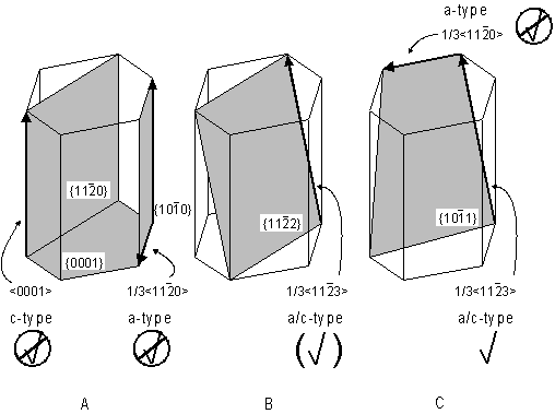
The slip systems to be expected in the wurtzite structure are shown schematically in Figure 11, with the basal plane being parallel to the heteroepitaxial interface. In Figure 12, the Peierls forces acting on dislocations in these slip systems are compared. A large Peierls force is expected in slip systems with a large Burgers vector, <0001> (c-type) or 1/3<11
Schematic of slip systems in the wurtzite structure. The basal plane is parallel to the heteroepitaxial interface. The crossed out ticks indicate slip systems that cannot lead to misfit dislocations by glide of threading dislocations. See 4.2 for details.
Peierls force as a function of the ratio of slip plane distance d and length b of the Burgers vector for the slip systems illustrated in Figure 11.

However, some slip systems can be ruled out as sources of misfit dislocations, simply because they do not provide a component of the Burgers vector lying in the interfacial plane. This is true for all slip systems with c-type Burgers vector (schematic A in Figure 11). Those with the slip plane being at right angles with the interface are inoperative, because there is no driving shear force acting on such a slip plane ({11
For the remaining 1/3<11
Calculated critical thickness hc of the InGaN layer as a function of the In content for nucleation of misfit dislocations by glide of 1/3<11

It was shown that TEM analyses of the threading dislocations in our samples reveal the presence of dislocations with mixed Burgers vector (Figure 8). They are the ones that have been considered as potential sources of misfit dislocations. As these dislocations do not end at the general sample surface, but at the pinholes, the effective length of the threading segment is even considerably smaller than the 100 nm that have been taken into account above.
Thus, within the given range of thicknesses and concentrations, misfit dislocations do not form by glide of pre-existing threading dislocations and subsequent deposition of misfit dislocation segments at the interface as in the Matthews-Blakeslee model. Instead, the few misfit dislocations that have been observed in the sample with the highest In content nucleate by a different mechanism and without prior motion through the heteroepitaxial InGaN layer: The deep pinholes that reach the heteroepitaxial interface serve as nucleation sites for these misfit dislocations, see TEM image in Figure 6 and schematic in Figure 14. The detected high stress at the apex of all pinholes at high In concentrations (Figure 5) results in a strain distribution that strongly deviates from that of a pseudomorphically strained two-dimensional layer. In particular, shear stresses are present in the (0001) plane that may cause activation and glide of dislocations in the 1/3<11
Schematic of plastic relaxation at deep pinholes that reach the heteroepitaxial interface, as observed in the sample with the highest In content of 14 %. Left: Cross-sectional schematic view of a deep pinhole, parallel to the heteroepitaxial interface (lower horizontal line). Right: Perspective view showing how the misfit dislocations glide away from the deep pinholes.

5. Summary
In conclusion, relaxation of misfit strain in the heteroepitaxial InGaN/GaN system has been investigated using TEM and AFM. It was shown that InGaN layers grow predominantly pseudomorphically up to the experimentally given layer thickness of 100 nm and In concentrations of up to 14 %. We detect an increase of the pinhole density with increasing In content of the InGaN layer and propose a model of elastic relaxation at pinholes. Application of the Matthews-Blakeslee model reveals, in accordance with the experimental results, that misfit dislocations do not form by glide of threading dislocations. Threading dislocations that are attached to pinholes always have a c-component Burgers vector, most of them are of mixed (a+c) type. In the sample with the highest given In content of 14 %, however, deep pinholes reaching the heteroepitaxial InGaN/GaN interface serve as nucleation sites for misfit dislocations. The slip system of these dislocations is 1/3<11
Thus, pseudomorphic growth of InGaN layers is rendered difficult by the deep pinholes. Those pinholes that do not produce misfit dislocations might be harmful as well. Some of the potential consequences are reduction of the diffusion length of free carriers, a higher density of surface states and composition inhomogeneities that may lead to carrier confinement as a consequence of elastic relaxation at pinholes. In order to avoid the presence of pinholes, further work on their formation mechanism is needed. On the one hand, our results and those reported in Reference Wu, Elsass, Abare, Mack, Keller, Petroff, DenBaars and Speck[6] already suggest that the strain field of the threading dislocations with a c-component Burgers vector is one of the factors that facilitate the formation of pinholes, where pinholes serve to reduce the misfit-induced strain. Thus the density of these threading dislocations needs to be reduced. On the other hand, it should be investigated whether pinholes only form beyond a critical thickness of the InGaN layer, as combined TEM and photoluminescence analyses of thick InGaN layers suggest Reference Hiramatsu, Kawaguchi, Shimizu, Sawaki, Zheleva, Davis, Tsuda, Taki, Kuwano and Oki[10].
Acknowledgments
This work has been partly supported by the German-American Cooperation Program (Deutscher Akademischer Austauschdienst and National Science Foundation).
Appendices
1 Equations used for the calculation of the critical thickness
For our calculations of the critical thickness hc according to the Matthews-Blakeslee model, we make use of the equations given in Reference Matthews and Matthews[8] and, for the Peierls force, in Reference Chidambarrao, Srinivasan, Cunningham and Murthy[9].
The force Fmisfit due to the misfit is given as

GInGaN is the bulk modulus and ν is Poisson's number of the InGaN layer, respectively. f is the misfit at the InGaN/GaN interface, b is the length of the Burgers vector, and l is the length of the threading segment in the heteroepitaxial layer. The Schmid factor S is dependent on the angle λ between the Burgers vector and a vector i, and on the angle β between the normal of the slip plane and the vector i. The vector i lies in the interfacial plane, perpendicular to the line of intersection of the interfacial plane and the slip plane.
The force Fline tension due to the line tension of the misfit segment is given as

GGaN is the bulk modulus of the thick GaN layer, serving as a substrate. h represents the thickness of the InGaN layer, and α is the angle between the Burgers vector and the line direction of the misfit segment.
The Peierls force FPeierls is given as

d is the spacing of the slip plane and χ the angle between the Burgers vector and the line direction of the threading segment. ω is a material constant given as

The number of atoms per unit cell is represented by n, the volume of the unit cell by V. T is the growth temperature of the InGaN layer in absolute degrees, k is Boltzmann's constant.
For the calculations, we neglect differences between the bulk moduli of the InGaN layer and GaN layer and use a value of 200 GPa for both, and take Poisson's number for InGaN as 0.6 Reference Wright[11].


