

1. Introduction
The GaN based semiconductors have recently been applied to fabricate optoelectronic devices such as light emitting diodes (LEDs) and laser diodes (LDs) in the blue and violet light region Reference Nakamura, Senoh and Mukai[1], Reference Nakamura, Senoh, Nagahama, Iwasa, Yamada, Matsushita, Kiyoku, Sugimoto, Kozaki, Umemoto, Sano and Chocho[2]. They also have the potential for electronic devices operating at high temperatures up to 300 °C due to their superior physical properties, such as the wide bandgap, high breakdown electric field, high saturation velocity, and high thermal conductivity Reference Khan, Shur, Kuznia, Chen, Burm and Schaff[3], Reference Aktas, Fan, Mohammad, Botchkarev and Morkoc[4]. To fabricate reliable, efficient, high-performance devices and circuits, it is essential to develop high quality and thermally stable contacts to GaN-based materials. Many extensive studies have been made for developing optimized ohmic contact systems Reference Liu and Lau[5], Reference Pearton, Zolper, Shul and Ren[6].
Since power dissipation across the p-GaN/metal interface generated Joule heat, failure of LDs was due to indiffusion of the ohmic contact elements along dislocations in the GaN epilayers, leading to the electrical short of the pn junction Reference Nakamura, Senoh, Nagahama, Iwasa, Yamada, Matsushita, Sugimoto and Kiyoku[7]. To employ metal layers as a reliable ohmic contact on GaN, it is essential to understand the thermal stability and metallurgy of metal-GaN contact in addition to developing low-resistance ohmic system. The research on the high temperature behavior, therefore, is the current interest.
Ni/Au has been commonly used as ohmic contact to p-type GaN in experimental LDs Reference Nakamura, Senoh, Nagahama, Iwasa, Yamada, Matsushita, Kiyoku, Sugimoto, Kozaki, Umemoto, Sano and Chocho[2], Reference Nakamura, Senoh, Nagahama, Iwasa, Yamada, Matsushita, Sugimoto and Kiyoku[7]. A low contact resistivity of around 10−3Ωcm2 was obtained for p-GaN after annealing in N2 ambient at temperatures ranging from 500 to 700 °C Reference Kim, Lee, Lee, Park and Kim[8]. The decrease of resistivity during annealing was explained due to the creation of Ga vacancies in p-GaN and the formation of Au-Ga solid solution from the x-ray diffraction data of reduced Au layer spacing. Systematic studies of the structural evolution and metallurgy are clearly needed, not only to examine thermal stability but also to understand the ohmic mechanism.
In this paper, we investigated the structural behavior of the Ni/Au contact on GaN(000l) during annealing in N2. GaN decomposition occurred mostly along GaN dislocations at temperature higher than 500°C. The decomposed nitrogen reacted with Ni and formed epitaxial Ni4N. At dislocation free regions, however, the atomically smooth interface remained intact up to 700 °C.
2. Experimental details
The GaN films were grown by metal-organic chemical vapor deposition (MOCVD) on c-plane sapphire substrate. An undoped GaN layer with a thickness of 2 μm was grown first, followed by the growth of 1.6 μm-thick p-type GaN doped with Mg. For deposition of Ni/Au films, the GaN samples were first cleaned with organic solvents, then etched in HCl:HNO3 (3:1) solution, and finally loaded into an e-beam evaporation system in which the base pressure was ~1×10⁻⁷ Torr. Ni (160 Å) and Au (200 Å) metals were deposited on p-type GaN in sequence.
The Ni/Au layers on p-GaN were studied using conventional XRD and synchrotron radiation techniques. The real time x-ray scattering measurements during annealing were performed using Cu K α radiation with a Huber diffractometer. All data for in-situ experiment shown in this paper were measured after holding for 30 min at each annealing temperature. The anomalous x-ray scattering (AXS) experiments were carried out at room temperature using synchrotron source at beamline 5C2 of Pohang Light Source (PLS) in Korea.
To examine the interfacial structures, high-resolution electron microscopy (HREM) studies were performed on the samples annealed at 550 and 700 °C for 1 min in a rapid thermal annealing (RTA) furnace under N2flowing atmosphere. Cross sectional samples were prepared as usual by mechanical thinning, followed by ion milling as the final step in order to obtain electron transparency. HREM observations were carried out along the GaN [1 1 −2 0] direction on a Topcon 002B electron microscopy operating at 200kV with a point to point resolution of 0.18nm (CS=0.4mm).
3. Results
We first examined structural evolution of Ni/Au layers on GaN (000l) during annealing using real time XRD. Figure 1 (a) shows a series of powder x-ray diffraction profiles (θ-2θscan) obtained during annealing in N2 at several temperatures. The scans were taken along the substrate surface normal direction, qZ, in reciprocal space. In the as-deposited film, the Au (111) and Ni (111) Bragg reflections appeared, indicating that the Au and Ni films were grown with the (111) preferred orientation. As the annealing proceeded up to 300 °C, the peak positions of the Au (111) and Ni (111) reflections were shifted to smaller qZ direction, which means the (111) layer spacing increased by thermal expansion. The interference fringes, observed in the wings of the Au (111) and the Ni (111) profiles for the as-deposited and 300 °C annealed samples, indicated that the layering of the aligned domains for Au and Ni was coherent throughout the whole thickness and the surface and interface of each aligned domain were atomically smooth. As the annealing temperature was raised higher than 350 °C, however, the Au (111) peak positions moved rather to the reverse direction. This indicated that the intermixing of the thermally activated Au and Ni atoms occurred and the pure Au and Ni phases were transformed to Au-rich and Ni-rich alloys, respectively. Meanwhile, the interference fringes were greatly reduced, which is another evidence of the intermixing. It is conceivable that the well-defined interface of Au and Ni will become rough during the intermixing along with the loss of the coherence.
The x-ray powder diffraction profiles along the surface normal qZ direction for the Au/Ni/GaN film measured during real-time annealing at several temperatures in N2. (b) The phi scans of GaN (1 0 −1 1) and Ni4N (1 1 −1) nonspecular reflections along the azimuthal direction for the figure 1 (a) sample after cooling. The well defined peaks indicate that Ni4N was grown epitaxially on GaN (000l).
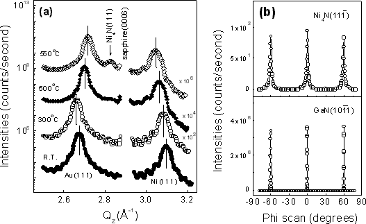
On the other hand, Ni4N phase nucleated at 500 °C, as revealed by appearance of Ni4N (111) Bragg reflection. We found the cubic Ni4N phase was grown epitaxially, which was confirmed by the nonspecular Ni4N (1 1 −1) reflection located 70.5° away from the surface normal direction. Figure 1 (b) shows the scattering profile along the phi scan of the nonspecular Ni4N reflection at room temperature. The well-defined peaks on the phi scans indicated that the Ni4N phase was in fact grown epitaxially on GaN (0001). From the relative directions of the film and the substrate crystalline axes, we summarized the epitaxial relationships of the cubic Ni4N phase as follows.
We note that the phi scan of the nonspecular Ni4N (1 1 −1) plane shows six-fold symmetry in Figure 1 (b), rather than three-fold symmetry. This was attributed to the six-fold symmetry of the GaN <1 0 -1 0> on the hexagonal substrate [ Figure 1 (b) ]. It is conceivable that the Ni4N (111) epitaxial domains are grown with the same probability along the GaN <1 0 -1 0> directions of six-fold symmetry. In the structural point of view, this is very similar to the cubic GaN <1 1 -1> with six-fold symmetry in the cubic GaN(111)/sapphire(0001) Reference Wu, Kapolnek, Tarsa, Heying, Keller, Keller, Mishra, DenBaars and Speck[9], Reference Cheng, Zhang, Zhang and Yu[10]. Au and Ni showed the same structural characteristics as Ni4N.
To clarify the existence of Ni4N phase more clearly, we carried out AXS experiments with synchrotron source at room temperature for the annealed sample of Figure 1 (a). We monitored the peak intensity of the Ni4N(111) while changing the x-ray photon energy around Ni K-edge absorption, 8.333 keV. The result is shown in Figure 2.
AXS result of the figure 1 sample after cooling. The momentum transfer was fixed to the position of the Ni4N (111) reflection and the scattering intensity was monitored as the x-ray energy was varied through Ni K-edge absorption.
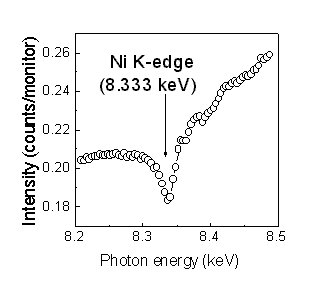
The atomic scattering factor, f ( = f0+ Δf ), consists of the nonresonant Thomson scattering factor, f0(Q), and the resonant anomalous scattering factor, Δf (k 1, k 2, E) which depends separately on the incident and scattered photon wave vectors k 1 and k 2, and on the photon energy E Reference Stragier, Cross, Rehr, Bouldin, Sorensen and Woicik[11]. In AXS measurements, the diffraction intensity is proportional to the square of the atomic factor and shows absorption-like information. Diffraction anomalous fine structure (DAFS) Reference Stragier, Cross, Rehr, Bouldin, Sorensen and Woicik[11], a technique combining diffraction and x-ray absorption fine structure (XAFS), can be used to selectively provide short-range order information of the long-ranged ordered atoms associated with a particular Bragg reflection, as well as the information on specific chemical valence and inequivalent atomic site.
For AXS measurements, the momentum transfer was fixed to the positions of the Ni4N (111) reflection and the scattering intensity was monitored as a function of x-ray energy in the vicinity of Ni K-edge absorption. If the element in question is related to the long-range order characterized by the specified Bragg peak, then the elemental absorption induces a decrease in the Bragg intensity at its absorption edge. A cusp, caused by the interference between the Thomson scattering amplitude and the real part of the anomalous scattering amplitude, is observed in the energy scan of the Bragg peak. Such behavior was indeed observed in Figure 2, indicating Ni was related to this Bragg peak. The result confirmed that the Bragg reflection originated from the Ni4N (111) planes.
To investigate the position of the decomposed Ga atoms, we performed AXS measurements around Ga K-edge absorption, 10.367 keV, for the (111) peaks of the Ni4N, the Au-rich alloy, and the Ni-rich alloy as shown in Figure 3. The cusps are observed only at the Bragg peaks for Au and Ni phases within our detection limit of AXS. The results indicate that Ga is related to the Bragg peaks for Au and Ni, while Ga is not associated with the Ni4N (111) Bragg peak. From these results, we conclude that the decomposed Ga atoms mostly diffuse into Au and Ni substitutional positions. The absence of Ga in the (111) Bragg peak of Ni4N suggested that Ga do not make a alloy with Ni4N.
AXS results of the figure 1 sample after cooling, Ga K-edge absorption. The momentum transfer was fixed to the position of the Ni4N (111), Au (111), and Ni (111) reflections, respectively.

To further understand the reacted interfacial microstructures, we carried out HR-TEM studies. Figure 4 (a) and (b) show the cross-sectional micrographs of the Au/Ni/GaN samples annealed at 550 and 700 °C for 1 min in a RTA furnace under N2flowing atmosphere, respectively. The metal indiffusion propagating along GaN dislocations (indicated by an arrow) was clearly shown in the 550 °C annealed sample. On the other hand, for dislocation free regions as illustrated in Figure 4 (b), atomically smooth interface remained even up to 700 °C. These results clearly indicate that GaN decomposition and reactions primarily concentrated on GaN dislocations.
Cross-sectional TEM image of GaN dislocation (indicated by an arrow) observed in the 550 °C annealed sample where metal indiffusion occurred. (b) HREM image of dislocation free region observed in the 700 °C annealed sample where atomically well defined interfacial structure is shown.

4. Conclusions
We have investigated details of the structural evolution of Ni/Au overlayers on GaN (0001) during the annealing process. Thermally activated atomic mobility caused metal atoms to interdiffuse and form solid solutions, at an annealing temperature higher than 350°C. The GaN decomposition and reactions occurred at 500°C, mostly along GaN dislocations. Decomposed Ga diffused into Ni and Au substitutional positions, and decomposed nitrogen reacted with Ni, forming Ni4N. Interestingly, the Ni4N was grown epitaxially. The orientation relationship of the Ni4N, Au, and Ni was identified as M(111)//GaN(0002) and M[1 −1 0] // GaN[1 1 −2 0] (M= Ni4N, Au, and Ni). At dislocation free regions, however, the atomically smooth interface remained intact up to 700 °C. To improve device reliability of the metal contact, metal indiffusion along GaN dislocations should be avoided.
ACKNOWLEDGMENTS
This work was supported in part by the Brain Korea 21 project and in part by the Korea Institute of Science and Technology Evaluation and Planning (KISTEP) through the NRL project.


