Introduction
It is our experience that atomic hydrogen readily permeates into GaN during many different device processing steps. The indiffusion is likely to be strongly enhanced by the presence of the high defect density in heteroepitaxial material. Examples of the processes in which hydrogen is incorporated into GaN at low temperatures (< 300 °C) include plasma enhanced chemical vapor deposition of dielectrics (the source of the hydrogen can be the plasma chemistry or erosion of the photoresist mask), boiling in solvents (including water), annealing under H2 or NH3 ambients and wet etching in acid or base solutions (e.g. NaOH, KOH). Secondary Ion Mass Spectrometry (SIMS) profiling after processing with deuterated chemicals to enhance the detection sensitivity show that hydrogen can diffuse into GaN at temperatures as low as 80 °C. The main effect of the hydrogen is passivation (electrical deactivation) of Mg acceptors in p-GaN through formation of neutral Mg-H complexes, which can be dissociated through either minority carrier (electron) injection or simple thermal annealing. There is evidence that all of the acceptor species in GaN, namely Mg, C, Ca and Cd are found to form complexes with hydrogen.
In this paper we will summarize what is known about the effects of hydrogen in GaN and discuss new results on the incorporation of hydrogen in electronic device structures.
Present State of Knowledge
The following information is firmly established for the behavior of hydrogen in GaN.[Reference Pearton, Zolper, Shul and Ren1-Reference Van Vechten, Zook, Horning and Goldenberg26]
-
GaN(Mg) grown by atmospheric pressure Metal Organic Chemical Vapor Deposition is highly resistive due to formation of neutral Mg-H complexes.[Reference Amano, Kito, Hiramatsu and Akasaki18,Reference Nakamura, Iwasa, Senoh and Mukai21,Reference Nakamura, Mukai, Senoh and Iwasa22] The Mg can be activated (i.e. produce p-type conductivity) by post-grown annealing at ≥ 700 °C in N2[Reference Nakamura, Mukai, Senoh and Iwasa22], low energy electron-beam irradiation near room temperature[Reference Amano, Kito, Hiramatsu and Akasaki18] or by forward biasing of a p-n junction to inject minority carriers (electrons).[Reference Pearton, Lee and Yuan27]
-
Thermal annealing in NH3 at ≥ 400 °C causes the GaN(Mg) to revert to a highly resistive (> 106 Ω⋅cm) state.[Reference Nakamura, Iwasa, Senoh and Mukai21,Reference Nakamura, Mukai, Senoh and Iwasa22]
-
GaN(Mg) grown by low-pressure MOCVD, Reactive Molecular Beam Epitaxy (solid Ga, NH3 gas) or by plasma-assisted MBE (solid Ga, plasma N2) can be p-type without annealing. This is presumably due to the lower H2 fluxes during growth, and the vacuum anneal undergone by RMBE material which is typically cooled without the plasma on.[Reference Popovici, Morhoe and Pearton28]
-
The residual hydrogen concentration in all GaN(Mg) tracks the acceptor concentration.[Reference Ohba and Hatano12]
-
All acceptor species show pairing with hydrogen (i.e. Mg, Zn, C, Ca, Cd).[Reference Lee, Pearton, Zolper and Stall13,Reference Amano, Kito, Hiramatsu and Akasaki18,Reference Nakamura, Iwasa, Senoh and Mukai21,Reference Amano, Akasaki, Kozawa, Sawaki, Ikeda and Ishii29-Reference Burchaid, Deicher, Forkel-Wirth, Haller, Magerle, Prospero and Stotzler31]
-
Donor dopant-hydrogen complexes have not yet been detected, and hydrogen concentrations are generally much lower in n-type GaN than in p-type material.[Reference Johnson, Gotz, Neugebauer and Van de Walle32]
-
Hydrogen enters GaN during many different device processing steps, even at 100 °C or lower.[Reference Pearton, Abernathy, Vartuli, Lee, MacKenzie, Wilson, Shul, Ren and Zavada11]
Information that is not as firmly established includes the following:
-
The energy levels and charge states (Ho, H+, H−) of hydrogen in GaN.
-
The existence of hydrogen molecules or larger clusters.
-
The role of hydrogen in facilitating p-type doping. Van Vechten[Reference Van Vechten, Zook, Horning and Goldenberg26] has suggested that hydrogen compensates native defects, making p-type doping possible, while Neugebauer and Van der Walle[Reference Neugebauer and Van de Walle14,Reference Van de Walle19] built on an earlier idea of Neumark’s[Reference Neumark33] from II-VI compounds that the presence of hydrogen increases Mg solubility and decreases compensating native vacancy defect concentration in GaN.
-
The role of line and point defects in enhancing hydrogen diffusivity (this will be answered by a comparison of its incorporation in the new epitaxial lateral overgrowth material with conventional heteroepitaxial GaN).
-
Hydrogen solubility – as with other semiconductors, the apparent solubility at low temperatures (≤ 500 °C) is likely to be dominated by the concentration of sites to which the hydrogen can be bonded, i.e. dopants, defects and impurities.[Reference Pearton, Corbett and Stavola34] In the following sections we will cover the incorporation of hydrogen during growth and processing, its thermal stability in GaN and some of the complexes it forms with dopants and defects.
Hydrogen in as-Grown GaN
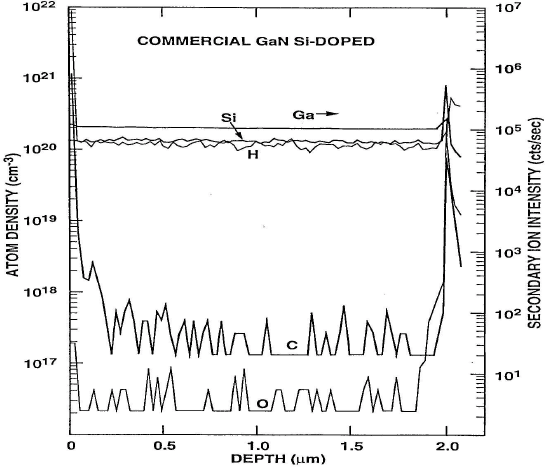
As mentioned above, the hydrogen concentration in p-GaN tracks the Mg concentration, and is correlated with the active Mg, not the total Mg density. Since Mg has a relatively deep ionization level (160-170 meV), the hole concentration at room temperature is typically only a percent or so of the total Mg in the crystal. We have found typical hydrogen concentrations in the 1018−1019 range in virtually all GaN grown by gas-phase techniques; in some samples doped with Si, we have seen the hydrogen present at higher concentrations (1020 cm−3), similar to that of the Si (Figure 1). This suggests the possibility of (Si-H) pair formation, but more work must be done to confirm this idea. It is a general result in semiconductors that acceptor passivation by hydrogen is more thermally stable than donor passivation and therefore is more readily observed experimentally.[Reference Pearton, Corbett and Stavola34]

Figure 1. SIMS profiles of H and other background impurities in MOCVD-grown, Si-doped GaN.
For the case of p-GaN, the hydrogen concentration is usually the same as the active Mg (i.e. ∼ 1% of 1020cm−3) after growth. A 700 °C, 20 min post-growth anneal in N2 only reduces the hydrogen concentration by a factor of 2 or 3, but this is enough to have strong p-type conductivity. An interesting question is whether the hydrogen is present in the GaN at the growth temperature (where it would be unbound and extremely diffusive) and then settles on the Mg during cooldown, or whether it actually enters the GaN from surface cracking of NH3 (to N2, NHx and H) during cooldown after growth (probably in the temperature range 300-600 °C). The latter is the passivation mechanism in p-type InP and GaAs grown by MOCVD, where hydrogen is found to deactivate 10-60% of Zn or C acceptors.
The annealing ambient may also affect the apparent thermal stability of the passivation, with reactivation of passivated Mg occuring at lower temperatures for N2 anneals. This is also a familiar phenomenon from other semiconductors. Since reactivation of the acceptor only requires dissociation of the Mg-H complex and a short range diffusion of the hydrogen away from the acceptor, it is also found that the apparent reactivation temperature depends therefore on the doping concentration (and therefore the associated hydrogen concentrations) and the layer structure and thickness (e.g. heteroepitaxial materials cladding the p-GaN layer may serve to retard hydrogen out-diffusion).
In contrast to other semiconductors in which acceptors are passivated by atomic hydrogen occupying a bond-centered position between the dopant and a neighboring lattice atom, in GaN the ionicity of the bonds means there is no local maximum in the charge density at the bond center. Both theoretical[Reference Neugebauer and Van de Walle14] and experimental[Reference Gatz, Johnson, Bour, McCluskey and Haller23] evidence suggests that in GaN(Mg) the hydrogen attaches to a nitrogen atom in an antibonding orientation. The predicted stretch frequency of hydrogen in the Mg-H complex is 3360 cm−1,[Reference Neugebauer and Van de Walle14] similar to that in NH3 molecules (3441 cm−1). Experimentally, a frequency of 3125 cm−1 has been reported.[Reference Gatz, Johnson, Bour, McCluskey and Haller23]
Hydrogen in as-Grown Device Structures
There is a lot of interest in the development of GaN-based high power, high temperature electronics for power switching and microwave applications. One potential device for ultra-high power switching is a thyristor, in either the npnp or pnpn configurations. Figure 2 shows a SIMS profile of Mg and H in an MOCVD-grown npnp thyristor structure. Note how the residual hydrogen tracks the Mg. Since the Mg-doped layer at ∼ 5.5 µm depth was the first to be grown, it contains less hydrogen than the Mg-doped region nearer to the surface which has spent less time at the growth temperature of 1040 °C. The source of the hydrogen is either the precursors, (CH3)3Ga and AsH3, or the carrier gas, which is generally H2. Sugiura et.al.[Reference Sugiura, Suzuki and Nishino17] found that if they employed a N2 carrier gas, they could get p-GaN without post-growth annealing. They also found that using a mixed H2/N2 carrier gas reduced the p-type doping level in as-grown samples. These results implicate the H2 carrier gas as the main source of hydrogen for passivation of the Mg acceptors, but previous experience in MOCVD growth of highly doped p-GaAs suggests that both the (CH3)3Ga and AsH3 are likely to also play a role. In particular, the cool down in AsH3 ambient after growth is likely a source of hydrogen for passivation.

Figure 2. SIMS profiles of H and other background impurities in an MOCVD-grown npnp thyristor structure.
Schottky and p-i-n diodes are employed as high-voltage rectifiers in power switching application. To suppress voltage transients when current is switched to inductive loads such as electric motors, these diodes are placed across the switching transistors. The advantage of simple metal-semiconductor diodes relative to p-n junction diodes is the faster turn-off because of the absence of minority carrier storage effects and lower power dissipation during switching. Wide bandgap semiconductors such as GaN offer additional advantages for fabrication of diode rectifiers, including much higher breakdown voltages and operating temperatures. There is much interest in developing advanced switching devices and control circuits for CW and pulsed electrical sub-systems in emerging hybrid-electric and all-electric vehicles, more-electric airplanes and naval ships and for improved transmission, distribution and quality of electric power in the utilities industry. Eventually one would like to reach target goals of 25 kV stand-off voltage, 2 kA or higher conducting current, forward drop less than 2% of the rated voltage and maximum operating frequency of 50 kHz.
Figure 3 shows a SIMS profile of H and other background impurities (along with intentional Si doping) in an MOCVD-grown p-i-n diode structure (left), together with the Mg profile in the structure (right). Notice once again that the H decorates the Mg due to formation of the neutral (Mg-H)o complexes. About 70-80% of the Mg atoms have hydrogen attached.
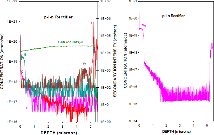
Figure 3. SIMS profiles of H and Si (left) and Mg (right) in an as-grown, MOCVD p-i-n rectifier structure.
To create a Schottky rectifier with high breakdown voltage, one needs a thick, very pure GaN depletion layer. Figure 4 shows SIMS profile of H and other background impurities in a 2 µm thick, high resistivity (107Ω⋅cm) GaN layer grown by MOCVD. The reverse breakdown voltage of simple Schottky rectifiers fabricated on this material was > 2 kV, a record for GaN. Notice that in this material the hydrogen concentration is at the detection sensitivity of the SIMS apparatus. The amount of hydrogen present in GaN after cooldown from the growth temperature will depend on the number of sites to which it can bond, including dopants and point and line defects. In the absence of p-type doping, it is clear that the number of these sites is ≤ 8×1017 cm−3 under our growth conditions.
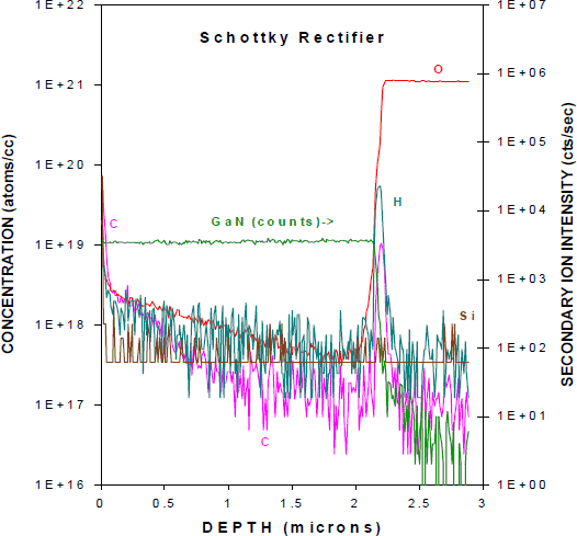
Figure 4. SIMS profiles of H and other background impurities in as-grown, MOCVD Schottky rectifier structure.
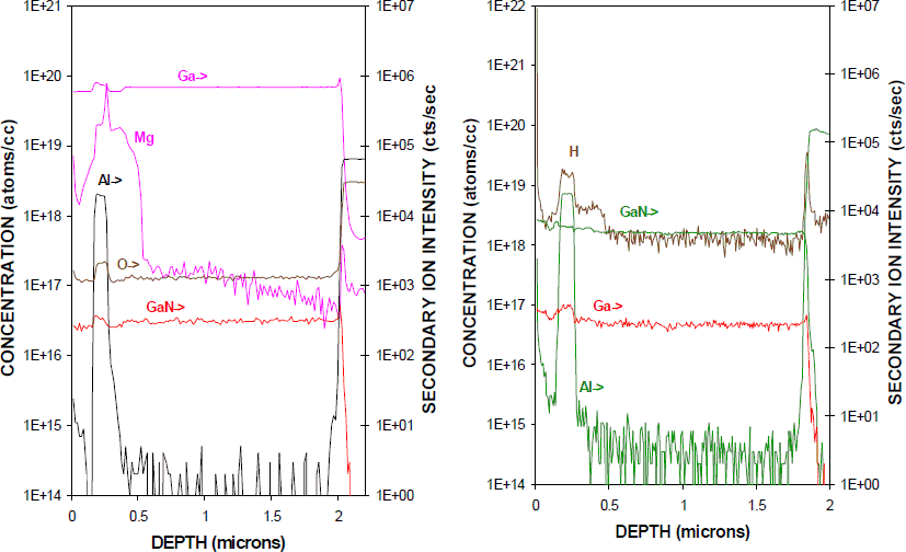
Another important device for power microwave applications is the heterojunction bipolar transistor (HBTs). Several groups have reported GaN/AlGaN HBTs with gains less than 10 at room temperature. Residual hydrogen passivation of the Mg acceptors in the base of such devices would create instabilities in the apparent gain during operation, since minority carrier injection would lead to time-dependent dopant reactivation, i.e. the gain would show an initial exponentially decreasing current gain, which might be interpreted as a reliability problem in the absence of an understanding of the effects of hydrogen. Figure 5 shows SIMS profiles of the Mg (left) and H (right) in an as-grown GaN/AlGaN HBT structure. The hydrogen is found to decorate both the GaN(Mg) base layer at ∼ 0.4 µm depth and also the AlGaN emitter layer, which is a region of additional strain within the structure.

Figure 5. SIMS profiles of Mg(left) and H (right) in as-grown MOCVD GaN/AlGaN HBT structure.
Once the device structure is grown and subsequently annealed to minimize the amount of residual hydrogen, there can still be problems associated with indiffusion during device fabrication. Atomic hydrogen is found to be unintentionally incorporated into the nitrides during many processing steps, including boiling in water, dry etching, wet etching, chemical vapor deposition of dielectrics and annealing in H2 or NH3. This shows that most of wet chemical or plasma processes involved in device processing are capable of causing passivation of dopants due to hydrogen incorporation in GaN and related alloys. SIMS profiling of GaN exposed to hydrogen-containing gases or chemicals shows that the hydrogen can diffuse into these layers at temperatures as low as 80 °C. Even though reactivation of dopants can be achieved by relatively low temperature thermal annealing after a given process step, the hydrogen may be cause similar problems after the subsequent processing so that one should be aware of its effects.
Diffusion of H in Implanted or Plasma-Treated GaN
Implantation of protons is commonly employed for inter-device isolation of electronic and photonic devices and for current guiding in various laser diode structures. Figure 6 shows SIMS profiles of 2H implanted into n-GaN, as a function of the subsequent annealing temperature under a N2 ambient. There is no redistribution of the deuterium until ≥ 800 °C, while at higher temperatures the remaining 2H decorates the implant damage profile which is slightly closer to the surface than the atomic profile. Note that even after a 1200 oC anneal there is a significant concentration of deuterium remaining at the peak of the damage profile. It appears that after high temperature annealing the deuterium is either trapped at defects or escapes the crystal.

Figure 6. SIMS profiles of 2H implanted into n-GaN at a dose of 2×1015 cm−2 and 50 keV, as a function of subsequent annealing temperature (10 secs. duration).
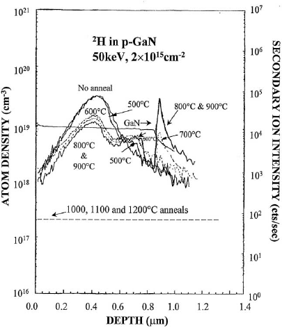
By sharp contrast, the redistribution of implanted 2H in p-GaN is more complicated. Figure 7 shows SIMS profiles of the deuterium as a function of annealing temperature. The redistribution begins at ≥ 500 °C and at higher temperatures there is decoration of the residual implant damage and the GaN/Al2O3 interface, in addition to the formation of a plateau region at ∼ 0.8 µm where Mg-H complexes are the dominant species. These results show that there is competition for trapping of deuterium between different sites, including strain and defects at interfaces, Mg dopants in the GaN, damage-related defects associated with the implant process and finally the surface of the GaN, through which the deuterium can evolve.

Figure 7. SIMS profiles of 2H implanted into p-GaN at a dose of 2×1015 cm−2 and 50 keV, as a function of subsequent annealing temperature (10 secs. duration).
An example of the indiffusion of deuterium into nitrides (in this case, AlN) as a result of exposure to a 2H plasma at low temperatures (200 or 250 °C) is shown in Figure 8. The deuterium has saturated the 1 µm thick layer after the 250 °C exposure. This gives a rough estimate for the diffusivity as 10−12 cm2⋅sec−1 at 250 °C. Similar values are obtained for deuterium in GaN. It is likely that the diffusivity in defect-free (bulk or homoepitaxial) nitrides is considerably lower than these values.

Figure 8. SIMS profiles of 2H in AlN exposed to deuterium plasmas at 200 °C or 250 °C for 30 mins.
Summary and Conclusions
Hydrogen is found to bond to regions of strain in GaN-based structures, such as interfaces or defects, as well as acceptor dopants. There are many potential sources of hydrogen during growth and processing of nitrides so that one needs to be vigilant for its effects, i.e. a reduction in hole concentration with an associated increase in hole mobility. It is expected that unintentional hydrogen incorporation will play a role in GaN electronic devices which contain p-n junctions, leading to high p-contact resistances and time-dependent current gains if precautions are not taken to remove the hydrogen.
Acknowledgements
The work at UF is partially supported by grants from DARPA/EPRI, MDA 972-98-1-0006, monitored by ONR (J.C. Zolper) and NSF 97-32865 (L. Hess). The work at NCU is partially supported by a grant from the National Science Council of R.O.C. under contract No. NSC-88-2215-E-008-012. Sandia is a multiprogram laboratory operated by Sandia Corporation, a Lockhead-Martin Company, for the US Department of Energy under contract No. DEAC04-94-AL85000. The work of RGW is partially supported by ARL (J.M. Zavada).