

 00> zone. Simulation was done by many-beam solution with 33 zero-order beams. The comparison of experimental CBED patterns and simulated patterns indicates that the polarity of GaN on Si(111) is Ga face.
Introduction
In recent years it has been demonstrated that GaN and related alloys grown by metalorganic vapor phase epitaxy exhibit superb properties for the design and production of light-emitting diodes and lasers operating in the short wavelength of the visible spectrum. LEO GaN on sapphire and silicon carbide substrates has been shown to result in a significant reduction of the extended defect density (3-4 orders of magnitude) which, in turn, has led to improvements in device performance for blue lasers, light-emitting diodes, p-n junctions, and field-effect transistors. For a review of relevant topics, see ref. [Reference Speck and Rosner1]. The success of LEO growth has revived interest in alternative substrates such as Si(111), which has potential advantages for device integration, thermal management, and cost issues. LEO GaN with low dislocation density on Si(111) substrates has recently been demonstrated [Reference Marchand, Zhang, Zhao, Golan, Rosner, Girolami, Fini, Ibbetson, Keller, DenBaars, Speck and Mishra2].
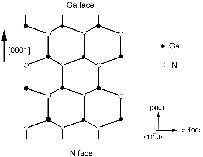
The most common growth direction for GaN is normal to the {0001} basal plane. The basal plane has a polar configuration with two atomic sub-planes each consisting of either the cationic or the anionic element of the binary compound. Thus, in the case of GaN a basal plane surface should be either Ga or N terminated (See Fig.1). Note that the polarity is a bulk property. The identification of the polarity in GaN can be carried out by several techniques such as X-ray photoemission spectroscopy [Reference Sasaki and Matsuoka3], convergent beam electron diffraction [Reference Liliental-Weber, Washburn, Pakula and Baranowski4,Reference Ponce, Bour, Young, Saunders and Steeds5,Reference Vermaut, Ruterana and Nouet6], and chemical etching [Reference Weyher, Müller, Grzegory and Porowski7]. For a review of GaN polarity determination, see ref. [Reference Hellman8]. In this paper we report on CBED studies of LEO GaN on Si(111) substrate and show that the polarity is Ga face.
<11
Experimental
Two inch-diameter Si(111) wafers were etched in buffered HF for one minute before growth. After heating to the growth temperature of 900°C under hydrogen, the TMAl and NH3 precursors were introduced in the MOCVD growth chamber and the AlN buffer layer was deposited at a total pressure of 76 Torr. The thickness of the AlN layer was ∼60 nm. The AlN layer was crack-free over the entire wafer, and the RMS roughness measured by AFM was on the order of 15 nm. The wafers were then coated with 200 nm-thick SiO2 using plasma-enhanced chemical vapor deposition, and 5 µm-wide stripes oriented in the Si<11
TEM samples were prepared by wedge polishing followed by Ar+ ion milling. Diffraction contrast images and CBED patterns were obtained on a JEOL 2000FX microscope operated at 200 kV. The surface topography was imaged using a Digital Instruments Dimension 3000 AFM operating in tapping mode. Simulations were done by software package “Desktop Microscopist 2.0” [9]. The simulated CBED patterns were calculated by solution of the many-beam equation with 33 zero-order reflections. It is well known that the polarity of GaN/Al2O3 grown by MOCVD is usually Ga face. We also checked the polarity of our MOCVD grown GaN on Al2O3 by CBED and confirmed that it is Ga face.
Results and Discussion
Cross-section TEM micrographs are shown in Figure 2. The seed region has a threading dislocation density on the order of ∼1011 cm−2, consisting predominantly of pure edge dislocations. In contrast, the LEO regions have a very low threading dislocation density and show an essentially single-crystalline microstructure. The plan-view TEM image (Figure 3) further confirmed that the threading dislocation density was reduced several orders of magnitude in the LEO region. No inversion domain boundaries were observed under both cross-section and plan-view TEM. We reasonably assume that the GaN/Si(111) grown by MOCVD has one unique polarity.
Cross-section bright-field TEM micrographs, g = 11

Plan-view bright field TEM image of LEO GaN/Si(111) clearly showing the seed (right) and overgrown region (left).

Figure 4 shows the comparison of experimental and simulated CBED patterns. The experimental CBED patterns were taken under <1
Experimental and simulated CBED patterns at different thickness. All patterns correspond to [1

Figure 5 shows the surface topography of LEO GaN grown on Si(111) over 144 µm2 area. Although the surface is undulated and shows spiral growth, the topography clearly consists of c/2-high atomic steps. In the seed region the pure screw and mixed-character threading dislocations (∼2×109 cm−2) are visible as surface depressions (∼20 nm in diameter) that terminate atomic steps. The lack of such step terminations in the LEO GaN regions clearly shows that the threading dislocation density is reduced significantly. Overall the surface is quite smooth. Our results are consistent with the framework summarized by E. S. Hellman [Reference Hellman8]: “smooth films grown by MOCVD are usually Ga face”.
Surface topography measured by AFM. The contrast is related to the amplitude of the tip vibration during tapping-mode imaging.

Conclusion
The polarity of MOCVD growth GaN/Si(111) with AlN buffer has been studied by convergent beam electron diffraction. Comparing the experimental patterns and simulated patterns, it is shown that the polarity of GaN film is Ga face.
Acknowledgements
This work was supported by the Office of Naval Research through a contract supervised by Dr. C. Wood and made use of the Materials Research Laboratory Central Facilities supported by the NSF under award No. DMR96-32716.


