

1. Introduction
GaN based semiconductors, over the last couple of years, developed from basic scientific research into a tremendous commercial market. As a key technology for full color displays and high temperature electronics, GaN needs no further introduction to motivate research in this field. Today, the growth of GaN and its related compounds is dominated by metal organic vapor phase epitaxy (MOVPE) Reference Nakamura, Senoh, Iwasa and Nagahama[1] Reference Koike, Sibata, Yamasaki, Nagai, Asami, Kato, Koide, Amano and Akasaki[2], a technique with an obvious advantage in fields where high throughput is required, e.g. for mass product such as light-emitting diodes (LEDs). However, even the quality of GaN layers grown by MBE is in many terms inferior to the best MOVPE results reported today. Therefore, the potential advantages of the MBE approach, well regarded from many other III-V semiconductor systems did not turn into real benefits for nitride semiconductor. Those inherent advantages include in-situ analysis by RHEED and mass spectrometry, as well as significantly reduced growth temperatures which decrease the residual strain and improve interface and doping profiles by a reduced diffusion. In conjunction with the lower precursor consumption and therefore reduced pollution MBE is attractive for industrial applications if layer qualities comparable to MOVPE can be achieved. We propose that the On-surface Cracking (OSC) approach, presented in this paper could be a significant progress for MBE in the field of GaN based semiconductors.
2. Growth Kinetics Using NH3
To understand why conventional GaN MBE could not turn its theoretical benefits into real advantages, the growth mechanisms of plasma-MBE have to be analyzed first. From this, the differences to the OSC approach become clear. To gain insights into the on-surface cracking of ammonia, we discuss the dissociation of ammonia under thermodynamic equilibrium, describe experimental results on the catalytic dissociation and will subsequently present GaN growth studies.
2.1 GaN growth by plasma MBE
In MBE, the most commonly used nitrogen precursor is molecular nitrogen (N2) where the high binding energy (9.5 eV) of the threefold nitrogen bond requires the use of a plasma cracking source. Plasma sources employ DC, RF or ECR plasmas to dissociate the nitrogen molecules thereby generating mostly highly reactive atomic nitrogen. The various plasma sources use different physical principles for plasma generation and have therefore different advantages and disadvantages. These aspects can not be discussed in detail here, however, the rather sophisticated plasma sources suffer to different extends from ion damages, contamination by sputtering effects, a lack of reproducibility and low growth rates. The different plasma sources have the common aim to dissociate the N2 molecule into a reactive species which becomes the nitrogen source for the GaN growth. This species is mostly atomic nitrogen (N). Since in MBE the mean free path is longer than the distance between plasma source and the substrate, those reactive species impinge to the growing surface. This highly reactive group V species makes GaN MBE distinctly different to MBE of conventional III-V semiconductors. Here, the group V precursor is supplied as a molecule (As4, As2, P2, etc.) which requires further reactions with the group V and group III elements before incorporation. Such reactions obviously provide a sufficient mobility of the species involved and require a group V rich growth regime for best growth conditions. The atomic nitrogen supplied in case of plasma MBE is that reactive, that it is supposed to react directly with every species on the surface, a situation quite different to the common MBE growth mode. It obviously implies different growth modes, too, since with plasma MBE good results are reported only for Ga-rich growth conditions Reference Riechert, Averbeck, Graber, Schienle, Strauß and Thews[3]. The effect of the V/III ratio on the crystal properties is dramatic and even a short period of group V terminated growth results into unrecoverable damage to the optical and electrical layer qualities. The growth modes are not fully understood yet, however, from conventional III-V epitaxy it is know that the surface mobilities are quite different on group III and the group V terminated surfaces.
Using NH3 as nitrogen precursor in the On-surface Cracking approach, where uncracked ammonia is supplied to the surface for GaN growth, the situation is much more similar to conventional MBE or to MOVPE of GaN. With OSC of ammonia, the best GaN properties are achieved using group V terminated growth as is shown below.
2.2 NH3 Dissociation under thermal equilibrium
To evaluate the suitability of ammonia for MBE growth first we assume thermodynamic equilibrium conditions for simplicity. The ammonia dissociation is determined for the relevant pressures and temperatures for the reaction:
Therefore, we assume that at T = 0 K a constant volume is filled with ammonia at the concentration [NH3]0. With increasing temperature the ammonia begins to dissociate into N2 and H2. The temperature and pressure dependent concentrations of [NH3], [N2] and [H2] can be calculated solving the three equations

Equation 2 describes the conservation of the total number of N atoms, equation 3 the conservation of the H2/N2 ratio and equation 4 is the mass action law Reference Mortimer, Chemie and Tieme Verlag Stuttgart[4]. The equilibrium constant KP (T) can be taken from the literature Reference Meyer[5], but has to be converted to K C which is necessary for the constant volume and variable pressure conditions of our experiment. Together with the ideal gas equation and after simple calculus the following expression of the ammonia dissociation D(T) can be obtained

The resulting data are shown in Figure 1. The NH3 dissociation under thermal equilibrium is given for two different concentrations, the left hand solid curve holds for MBE conditions at the growth surface (1×10⁻⁵ mbar, T = 1000 K, corresponding to a concentration of 3×10⁻¹¹ mol/l). The thermal equilibrium calculations yield an almost complete dissociation above approx. 200 K. The right hand solid curve is computed for MBE conditions in the gas injector (1×10⁻² mbar, T = 600 K, corresponding to a concentration of 2×10⁻⁷ mol/l). An almost complete dissociation is found above approx. 300 K. The dashed curve represents experimental data obtained for ammonia dissociation in the MBE gas injector. Here, temperatures around 1100 K are required to achieve an almost complete NH3 dissociation under non-equilibrium conditions. The difference between thermal equilibrium calculations and experimental data for injector cracking reveals that the ammonia dissociation is not in thermal equilibrium, but limited by a kinetic barrier. This barrier can be reduced by a catalyst, thereby shortening the time until thermal equilibrium is established. Therefore, the catalyst pushes the dynamic equilibrium towards dissociation. Under experimental conditions where the thermal equilibrium is not achieved a catalyst improves the ammonia dissociation. However, a catalyst cannot shift the position of the final, stationary thermal equilibrium, since both forward and backward reaction are enhanced.
Temperature dependent NH3 dissociation under thermal equilibrium and under experimental, non-equilibrium conditions (see text).

2.3 Catalytic NH3 Dissociation
The catalytic dissociation of ammonia is investigated using the high temperature gas injector of the MBE system, a Riber HTI 432 injector (Figure 2). A quadrupole mass spectrometer (QMS) is employed to measure the NH3 dissociation. The QMS has only a limited sensivity since it does not measure directly in the molecular beam. After correction for the cracking pattern, we found no evidence for reactive nitrogen species such as N or NH within the detection limit. At temperatures above 1100 K a weak NH2 signal is found, where it is not clear whether this corresponds to the occurrence of NH2 or is an artifact of the correction for the cracking pattern. We assume that the overall reaction inside the injector can be described by the dissociation of NH3 into molecular N2 and H2. This is in good agreement with our expectations since the free path length within the injector is approx. 10 mm, leading to a fast neutralization of reactive species inside the injector. Important insights into the mechanisms of ammonia dissociation are obtained by flux dependent studies. Figure 3 shows the Arrhenius plot of the total amount of dissociated NH3 which is fairly independent on the supplied amount of NH3 over a wide range of temperatures (T ≤ 950 K) and fluxes. In this regime, a kinetic limitation of the process is observed, whereas at higher temperatures the dissociation saturates and the total number of dissociated NH3 is determined by the supplied fluxes. The dissociation cannot be pyrolytic only, since we obtain an upper limit in the kinetically limited region, where the total dissociation is independent on the flux. This saturation can be explained with the following catalytically enhanced dissociation model. We assume that the number of catalytic surface states is limited. During the dissociation process each state is occupied for a certain time τ0. At low fluxes all ammonia molecules find a vacant surface state to dissociate. The collision rate of ammonia with the surface is slower than the reaction rate of the dissociation process. With increasing flux the collision rate exceeds the reaction rate, excess ammonia does not find free surface states, the dissociation saturates and is independent on the total flux, as observed. Increasing temperature enhances the reaction rate between the catalytic surface states and the ammonia. The rate increases and free surface states become again available for dissociation. The overall process can be described by the transition function:

Temperature dependence of the ammonia dissociation in the gas injector.

Arrhenius plot of the NH3 dissociation. Symbols indicated experimental data, solid lines are calculated according to equation 6

Q is the supplied NH3 flux, Γ is a constant depending on the density of the surface states, the active surface area of the injector and a factor describing the efficiency of the adsorption process. Whereas Q is given by the experiment, Γ is used as a fitting parameter for equation 6. T 0 is the transition temperature which is determined to 950 K from the fit. The activation energy E a of the kinetically controlled process is 1.2 eV. With this data we find an excellent agreement between experiment (symbols in Figure 3 and our model (solid lines in Figure 3)). The catalytic reaction is assumed to take place at the three molybdenum disks which act as baffle in the injector's orifice (molybdenum is a well-known catalyst for ammonia).
The above presented model is consistent with results obtained from dedicated surface science studies investigating the catalytic reaction between NH3 and polycrystalline steel (Fe), powdered tungsten (W) and molybdenum (Mo), Reference Ertl and Huber[6] Reference Tamaru[7] Reference Grunze and King[8]. These studies reveal that NH3, after physisorbtion to the surface, instantaneously chemiosorbs under release of a hydrogen atom at temperature above 200 K. At moderate temperatures NH2 and NH are formed, H2 is released from the surface. With increasing temperatures the remaining H is stripped off and the nitrogen forms a nitride with the surface. At high temperatures and sufficient ammonia fluxes such nitride layers may reach a thickness of several monolayers. Nitrogen molecules then evaporate by decomposition of the nitride as is concluded from the desorption energy which is the dissociation energy of the particular nitride rather than the binding energy of the nitrogen bonded to the surface (Figure 4). Differences in catalytic efficiency are due to the differences in the stability of the corresponding metal nitrides. Later is governed by the reaction between the unoccupied d-orbitals of the metal surface and the free electron pair of the ammonia molecule.
Surface reactions of ammonia on a catalytic surface.

The experimental results have the following implications to epitaxial growth:
-
• NH3 dissociation is sufficient under growth conditions.
-
• The surface is supposed to be NHx terminated.
-
• The effective V/III ratio on the surface should be fairly independent of the supplied V/III flux ratios over a wide range.
2.4 Growth kinetics of GaN using NH3
Above results suggest that the surface is covered with nitrogen under regular growth conditions, corresponding to a group V rich surface. This growth mode is common in conventional III-V growth, but is in distinct difference to the MBE growth of GaN with plasma MBE Reference Riechert, Averbeck, Graber, Schienle, Strauß and Thews[3]. The observed linear dependence of our GaN growth rate on the supplied Ga flux is a further indication for a group V rich surface. The extrapolation of the growth rate to zero Ga flux (the intercept with the y-axis) has to be interpreted as the Ga desorption (Figure 5). At a growth temperature of 750°C the intercept is −250 nm/h which is consistent with the observed Ga desorption at this temperature (see Figure 6). A significant Ga desorption starts at temperatures above 500°C, the activation energy is surprisingly low with 0.65 eV. Ga desorption is significant at regular growth conditions (≈ 30 %). The knowledge on NH3 dissociation, the kinetic limitation of the catalytic processes and the Ga desorption is summarized in a diagram (Figure 7). Here, the different relevant mechanisms and limitations for the on-surface cracking (OSC) approach of ammonia in GaN MBE versus growth temperature.
Dependence of the GaN growth rate on the supplied Ga flux at 750°C.

Dependence of GaN growth rate on temperature.

Relevant OSC growth regimes versus temperature of growth.

3. Growth of Group III-Nitrides
Using on-surface cracking of ammonia for MBE growth we describe the relevant growth parameters and crystal properties for GaN, InGaN and AlGaN. First results on homoepitaxial growth of GaN will also be discussed.
Our otherwise standard MBE system (Riber 32) was adapted to group V gas sources. The system is turbo pumped, the attached gas control and handling system are home made. NH3 is introduced into the system through a standard high temperature injector (Riber HTI 432). Effusion cells are used to supply group III species (Al, Ga, In) and dopants (Si, Mg). Unless otherwise mentioned GaN layers are grown on c-plane oriented sapphire at growth rates of 750 nm/h to a thickness of approximately 1.8 μm.
3.1 GaN
The heteroepitaxial growth of GaN on c-plane sapphire requires decent preparation steps before subsequent growth of the GaN layer. Many authors have reported different approaches of sapphire preparation and nucleation layer growth Reference Nakamura, Mukai and Senoh[9] Reference Uchida, Watanabe, Yano, Kouguchi, Tanaka and Minagawa[10].
The following procedure provided the best results at our laboratory and therefore was used for our experiments (Figure 8):
-
1. The sapphire is heated up to approx. 850°C and kept at this temperature for 5 minutes under a certain NH3 flux.
-
2. The substrate is lowered down to 700°C for the nucleation layer growth. At this temperature a 5 nm AlN layer is deposited, followed by a 15 nm GaN layer. Subsequently, the layers are annealed at 770°C for 5 minutes.
-
3. The substrate is lowered o 750°C before GaN growth is initiated.
Depiction of the thermal cycling during MBE growth using OSC.

The influence of the initial steps of growth, especially of the nitridation step and the deposition of the nucleation layer, is depicted in Figure 9. Here, the photoluminescence of a 2 μm thick GaN layer grown under standard conditions is shown. The only differences are the utilization of nitridation and nucleation layer, a nucleation layer only and a nitridation step only, respectively. At a growth rate of 750 nm/h and with application of nitridation and nucleation layer we achieve the following crystal properties for a GaN layer with a thickness of 1.8 μm. :
-
• Low-temperature photoluminescence dominated by donor bound excitons (DBE), linewidths of 5 meV at 4 K (Figure 10)
-
• Carrier concentrations of 2×1017 cm−3 with carrier mobilities of μ = 220 cm2/Vs at 300 K. Free carrier concentrations down to 1016 cm−3 have been achieved. However, carrier mobilities of μ μ 100 cm2/Vs indicate highly compensated material.
-
• X-ray rocking curves with linewidths of 400-450 arcsec in an ω-scan of the (0002) reflex.
Influence of the initial stages of growth on the photoluminescence of the subsequently grown 2 μm thick GaN layer. Excitation density approx. 10 mW/mm2 at 325 nm.

Photoluminescence of GaN heteroepitaxially grown on sapphire. The transitions center at 3.4802 eV and 3.4776 eV with linewidths of 4.1 meV and 11.0 meV, respectively. Excitation density approx. 2 mW/mm2 at 325 nm.

3.2 AlGaN
AlGaN is grown by additional supply of aluminum under otherwise unchanged growth conditions. Depending on the Al-flux, AlN mol fractions up to 35 % have been realized.
AlGaN layers with an aluminum content of 17 % reveal free carrier concentrations of n = 1×1018 cm−3 with carrier mobilities of 10 cm2/Vs. The PL spectrum of an AlGaN layer is shown in Figure 11, where AlGaN is used as barrier for a GaN quantum well. The aluminum incorporation turns out to be a nonlinear function of the Al/Ga flux ratio carefully considering corrections due to different ionization probabilities and thermal velocities. The experimental data displayed in Figure 12 could be interpreted by competing chemical reactions between the two group III elements and ammonia. However, further work is required to clarify these experimental results.
Photoluminescence of an AlGaN/GaN quantum well. Excitation density approx. 2 mW/mm2 at 325 nm.
Aluminum/gallium ratio in AlGaN versus supplied aluminum/gallium ratio.

3.3 InGaN
The high vapor pressure of the elemental indium requires growth conditions different from those of GaN. The deposition temperature is reduced to 560°C to achieve measurable indium incorporation. The In/Ga ratio has to be increased to 15 to achieve an indium content of 4 % according to XRD. Room temperature PL shown in Figure 13 is still dominated by a rather broad transition at 3.06 eV indicating defect related luminescence. Further experiments have to be carried out to increase In concentration as well as to improve InGaN crystal quality.
Room temperature photoluminescence of InGaN. The transitions occur at 3.412 eV and 3.062 eV with linewidths of 78 meV and 152 meV, respectively. Excitation density approx. 10 mW/mm2 at 325 nm.

3.4 GaN-homoepitaxy
GaN growth on sapphire has proven its ability to yield excellent LEDs as well as GaN based lasers by decent preparation techniques such as nitridation, low temperature nucleation layer, etc. In spite of the amazing success of GaN based LEDs Reference Nakamura, Senoh, Iwasa, Nagahama, Yamada and Mukai[11] Reference Kong, Leonard, Bulman, Negley and Edmond[12] and lasers Reference Nakamura, Senoh, Nagahama, Iwasa, Yamada, Matsushita, Kiyoku and Sugimoto[13] both obtained by heteroepitaxial growth, homoepitaxy may overcome inherent problems of lattice mismatch, columnar growth, dislocations and thermal mismatch. Furthermore, GaN substrates are electrically conductive, allowing current injection through the substrate and have a sufficient thermal conductivity to facilitate high power applications. The Polish High Pressure Research Center for the first time produced GaN substrates in useful sizes up to 9 × 9 mm2 with thicknesses around 300 μm Reference Suski, Perlin, Leszczynski, Teissere, Grzegory, Jun, Bockowski, Porowski, Pakula, Wysmolek and Baranowski[14]. Employing high pressure (15000 bar) and high temperature (1600°C), GaN platelets were obtained from seeded and unseeded Ga melts under N2 pressure. Dislocation densities are in the 103 cm−2 range, whereas a high number of point defects still cause background carrier concentrations of 1019 cm−3.
Such crystals are the ideal test vehicle to investigate the potential of a certain growth technique since all problems related to nitridation and nucleation layers do not arise. For homoepitaxial growth, the as-grown (unpolished) GaN crystals were In-mounted to the Mo holder, heated up to 750°C under ammonia before growth was initiated under conventional growth conditions mentioned above Reference Teisseyre, Nowak, Leszczynski, Grzegory, Bockowski, Krukowski, Porowski, Mayer, Pelzmann, Kamp, Ebeling and Karczewski[15] Reference Mayer, Pelzmann, Kamp, Ebeling, Teisseyre, Nowak, Leszczynski, Grzegory, Bockowski, Krukowski, Porowski and Karczewski[16].
The curve in Figure 14 shows the excitonic region of a PL spectrum for 0.4 μm thin homoepitaxial GaN layer. The bound excitons transitions are much narrower than the transitions corresponding to free excitons. The transition of the acceptor bound exciton (ABE) at 3.4663 eV reveals a linewidth of 0.5 meV. The DBE lines at 3.4709 eV and 3.4718 eV have comparable linewidths, the separation is approximately 1 meV. The lines of the free excitons (FE) A (3.4785 eV) and B (3.4832 eV) and the yet unidentified line at 3.4735 eV show linewidths of about 2 meV. Neither strong yellow luminescence nor luminescence near 3.2 eV due to donor-acceptor pair transitions are observed. Figure 15 shows PL spectra at higher temperatures. The intensity of the FE A transition strongly increases with temperature and exceeds the DBE lines at 28 K. The intensity of the FE B increases with temperature, too, and at about 80 K the FE C becomes clearly visible. With increasing temperature the ABE transition becomes broader and weaker. The DBE transitions do not shift, but decrease in intensities. The line at 3.4735 eV undergoes significant changes. The intensity decreases with increasing temperature and nearly vanishes at 28 K. The crystal structure of the grown layers is examined by high resolution x ray diffraction. Using Cu Kα1 radiation a linewidth of approx. 20-30 arcsec is found for the (0004) Bragg reflex. The uncertainty arises from the convolution of the homoepitaxial layer and its substrate. A small difference of about 120 arcsec. in the lattice constants of layer and substrate reflects the high concentration of free electrons and point defects within the substrate crystal.
Photoluminescence of a 0.4 μm thin GaN layer grown on a GaN substrate. Excitation density approx. 0.5 mW/mm2 at 325 nm.

Photoluminescence of homoepitaxial GaN at elevated temperatures. Excitation density approx. 0.5 mW/mm2 at 325 nm.

4. Doping & Device Structures
Excellent results on the homoepitaxial GaN growth have proven that the OSC approach makes MBE a serious competitor to MOVPE for GaN growth. MBE specific advantages such as a reduced growth temperature, in-situ analysis and low precursor consumption and low pollution may become important aspects. It remains, however, to demonstrate device structures of comparable quality. Following, we present our work on p- and n-doping, quantum wells and LEDs.
4.1 P-doping
P-doping is one of the major challenges for fabrication of light-emitting devices in GaN. Early reports claimed that p-doping in MBE can only be achieved if a plasma source is used along with the ammonia Reference Yang, Li and Wang[17]. Whereas Wang et al. achieved free hole concentrations with simultaneous use of the plasma cell and ammonia, they could not achieve p-doping when ammonia was used alone.
We supplied Mg from an effusion cell for p-type doping under OSC conditions without any plasma source. P-doping was verified by several techniques, including hot probe and rectification methods, current-voltage characteristics and Hall measurements. Whereas the first two methods indicate the conductivity type only, Hall measurements yield hole concentrations in the midst 1016 cm−3 range, but do not always yield reasonable results. In spite of the presence of hydrogen during the growth process, p-conductivity is achieved without annealing, however, tempering at 750°C for 10 min seems to improve conductivity. Photoluminescence of Mg doped GaN is presented in Figure 16. As can be taken from the narrow well-resolved spectrum, the sample has a low Mg concentration, which is confirmed by secondary ion mass spectroscopy (SIMS) yielding a Mg concentration in the low 1019 cm−3 regime. The spectrum is dominated by a rather narrow transition at 3.26 eV and the corresponding LO phonon replica at lower energies. The Mg incorporation is governed by an almost exponential decrease with increasing temperature, where the activation energy for the Mg desorption is 2.56 eV (Figure 17). Mg desorption is the limiting mechanism under our experimental growth conditions. An effect of the increasing energy of formation which should yield a higher Mg incorporation at higher temperatures is not observed Reference Neugebauer and Van de Walle[18].
Photoluminescence of Mg-doped GaN. Excitation density approx. 10 mW/mm2 at 325 nm.

Temperature dependence of Mg incorporation into GaN.

4.2 N-doping
Silicon from a standard effusion cell is used as donor in our experiments. Doping was investigated up to free electron conchentration of n=4.5×1018 cm−3 with corresponding room temperature mobilities of 150 cm2/Vs. The PL spectrum however is still dominated by a bound exciton (DBE) as can be taken from Figure 18. Compared to undoped layers the photoluminescence intensity is strongly enhanced by a factor of 80. Microcracks as reported in literature have not been observed in the layers, probably due to the reduced growth temperature.
Photoluminescence of Si-doped GaN. Excitation density approx. 10 mW/mm2 at 325 nm.

4.3 Quantum Well Structures
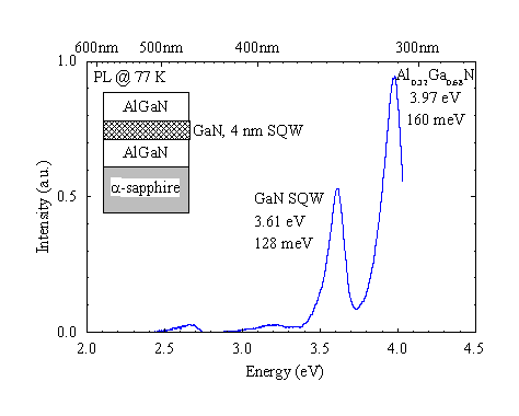
GaN single quantum well (SQW) structures have been grown with quantum well thicknesses of nominally 4 nm embedded in Al0.32Ga0.68N. Figure 11 shows the PL spectrum of the SQW and the AlGaN barriers. The quantum well luminescence is shifted by 150 meV. The photoluminescence of the 4 nm GaN layer is still broad at 128 meV. TEM and excitation spectroscopy can be used to determine if the broadening is due to interface fluctuations or higher sub-band emission.
4.4 Light-Emitting Diodes
Homotype pn-junction have been grown on sapphire. The layers were processed using CAIBE Cl2 etching, Ti/Au n-contact metallization and Ni/Au p-contact formation. Specific contact resistances are in the 10−5 Ωcm2 and 10−2 Wcm2 range for n- and p-contacts, respectively. Figure 19 depicts an I-V-characteristic of a MBE grown homotype LED. The high series resistance of the LED limits the current to about 20 mA at 20 V. The reason for the high series resistance, which is formed by the contact resistances and sheet resistances of the n- and the p-layers, is not clear, yet. Anyhow, at higher voltages (qU >> (nkBT)) the current passing through the device is no longer determined by the pn-junction, but limited by the series resistance. Here, the series resistance can be calculated to 250 Ω for the curve shown below. The turn-on voltage of the pn-junction is approx. 3 V, which can clearly be seen if current is plotted versus the voltage across the junction (U-RSI). The obtained electroluminescence is shown in Figure 20. An intense single peak emission at 374 nm, with a narrow linewidths of 12 nm (FWHM) is achieved. The high energy side of the spectrum, which is obtained through the n-GaN and the sapphire, is clearly determined by adsorption within the device. A modified vertical design of the LED has to avoid internal absorption to increase the output power of the device. The optical output power of the GaN homojunction LED is shown in Figure 21. The dependence of the optical power on the forward current follows a power law:
I-V-characteristic of a homotype GaN pn-junction.

Electroluminescence from a homotype GaN pn-junction (300 K).

Dependence of optical output power on forward current for a GaN homojunction LED.

Such a behavior is in accordance to the LED theory Reference Kressel and Buttler[19], which predicts an exponent between 1 and 2 for recombination by diffusion currents and recombination currents, respectively. An exponent of 1.2 as obtained for the above presented LED indicates the high quality of the MBE grown homojunction. At currents above 40 mA, the measured output power decreases which is attributed to thermal effects. Above results on MBE grown GaN LEDs are very encouraging, such structures can be used for the excitation of phosphoruses in white LEDs or for spectroscopic applications. For blue and green LEDs, however, indium has to be incorporated into the active region. Both LEDs, UV as well as visible, should benefit from the utilization of heterostructures and a further improvement of the p-doping.
5. Summary
On-surface cracking (OSC) of ammonia is presented for molecular beam epitaxy of GaN based structures. Outstanding photoluminescence results with linewidths as low as 0.5 meV are achieved by homoepitaxial growth of GaN. Heteroepitaxial growth of GaN on sapphire yields optical, electrical and structural properties comparable to MOVPE material. AlGaN has been grown with good material properties, whereas with InGaN further work is still necessary to achieve device quality material. P- and n-doping have been obtained using conventional Mg and Si effusion cells. Encouraging LED performances have been achieved from homotype pn-junctions, where narrow single peak emission at 374 nm is obtained with linewidths as narrow as 12 nm. Further improvements of MBE grown LEDs are expected by the application of heterostructures.
Apart from technological aspects, fundamental insights into the growth mechanisms of the OSC process have been presented. Thermodynamic equilibrium calculations, mass spectroscopy and kinetic studies were employed to obtain a detailed understanding of the underlying processes. Important mechanisms of ammonia dissociation as well as of the kinetics of GaN growth have been determined.
Acknowledgments
We would like to acknowledge valuable contributions and active support from A.Thies, C.Kirchner, M.Schauler, F.Eberhard, P.Unger as well as financial support from the German Ministry of education, science, research and technology (BMBF) and the Volkswagen Foundation. The work on the homoepitaxial growth was done in close cooperation with the High Pressure Research Center of the Polish Academy of Sciences namely with H.Teisseyre, G.Karczewski, G.Nowak, M.Leszczyski, I.Grzegory, and S.Porowski.


