


 d cubic on heating from room temperature to 733 K. On cooling to room temperature, the crystal structure reverts to I4
I. INTRODUCTION
Synthetic anhydrous analogues of the silicate framework minerals leucite (end-member KAlSi2O6) and pollucite (end-member CsAlSi2O6) can be prepared with the general formulae A 2BSi5O12 and ACSi2O6, where A is a monovalent alkali metal cation, B is a divalent cation, and C is a trivalent cation (Torres-Martinez and West, Reference Torres-Martinez and West1984, Reference Torres-Martinez and West1986, Reference Torres-Martinez and West1989; Torres-Martinez et al., Reference Torres-Martinez, Gard, Howie and West1984). These structures all have the same topology, with B and C cations partially substituting onto tetrahedrally coordinated sites (T-sites) in the silicate framework and charge-balancing A cations sitting in the extra-framework channels. The A cations can be replaced by ion exchange. Cs-containing silicate framework minerals are of potential technological interest as storage media for radioactive Cs from nuclear waste (Gatta et al., Reference Gatta, Rotiroti, Fisch, Kadiyski and Armbruster2008). A review paper on leucite crystal structures has been published (Bell, Reference Bell2025).
X-ray and neutron powder diffraction have been used to determine and refine the ambient temperature crystal structures of leucite analogues with the general formulae A
2BSi5O12 and ACSi2O6. Crystal structures have been refined in the Ia![]() d cubic and I41/a tetragonal space groups (A = K, Rb, Cs; B = Mg, Mn, Co, Ni, Cu, Zn; C = Fe3+, Ga; Bell et al., Reference Bell, Henderson, Redfern, Cernik, Champness, Fitch and Kohn1994a, Reference Bell, Knight, Henderson and Fitch2010; Bell and Henderson, Reference Bell and Henderson1994a, Reference Bell and Henderson1994b, Reference Bell and Henderson2018, Reference Bell and Henderson2020; Bell and Stone, Reference Bell and Stone2021). These structures all have disordered T-site cations and have A cation sites fully occupied with either K, Rb, or Cs. CsGaSi2O6 also has a disordered T-site structure in the space group
d cubic and I41/a tetragonal space groups (A = K, Rb, Cs; B = Mg, Mn, Co, Ni, Cu, Zn; C = Fe3+, Ga; Bell et al., Reference Bell, Henderson, Redfern, Cernik, Champness, Fitch and Kohn1994a, Reference Bell, Knight, Henderson and Fitch2010; Bell and Henderson, Reference Bell and Henderson1994a, Reference Bell and Henderson1994b, Reference Bell and Henderson2018, Reference Bell and Henderson2020; Bell and Stone, Reference Bell and Stone2021). These structures all have disordered T-site cations and have A cation sites fully occupied with either K, Rb, or Cs. CsGaSi2O6 also has a disordered T-site structure in the space group $ I\overline{4}3d $
(Bell and Stone, Reference Bell and Stone2021). Crystal structures have also been refined at ambient temperature for P21/c monoclinic crystal structures of leucite analogues with the general formulae A
2BSi5O12 (A = K; B = Mg, Fe2+, Co, Zn; Bell et al., Reference Bell, Henderson, Redfern, Cernik, Champness, Fitch and Kohn1994a; Bell and Henderson, Reference Bell and Henderson2018) and also for Pbca orthorhombic (A = Rb; B = Mg, Mn, Ni, Cd; Bell and Henderson, Reference Bell and Henderson1996, Reference Bell and Henderson2009, Reference Bell and Henderson2016) and (A = Cs; B = Mg, Mn, Co, Ni, Cu, Zn, Cd; Bell et al., Reference Bell and Henderson1994b; Reference Bell, Knight, Henderson and Fitch2010; Bell and Henderson, Reference Bell and Henderson1996, Reference Bell and Henderson2009). These structures all have ordered T-site cations and have A cation sites fully occupied with either K, Rb, or Cs. RbCsX
2+Si5O12 (X = Mg, Ni, Cd) leucite analogues, with two different extra-framework alkali metal cations, all have the Pbca structure with ordered T-site cations (Bell and Henderson, Reference Bell and Henderson2019). For X = Ni and Cd, these structures have disordered extra-framework cations, but for X = Mg, there is partial ordering of the extra-framework cations. Cs2X
2+Si5O12 (X = Cd, Cu, Zn) all retain the cation-ordered Pbca orthorhombic structure below 10 K (Bell, Reference Bell2021).
$ I\overline{4}3d $
(Bell and Stone, Reference Bell and Stone2021). Crystal structures have also been refined at ambient temperature for P21/c monoclinic crystal structures of leucite analogues with the general formulae A
2BSi5O12 (A = K; B = Mg, Fe2+, Co, Zn; Bell et al., Reference Bell, Henderson, Redfern, Cernik, Champness, Fitch and Kohn1994a; Bell and Henderson, Reference Bell and Henderson2018) and also for Pbca orthorhombic (A = Rb; B = Mg, Mn, Ni, Cd; Bell and Henderson, Reference Bell and Henderson1996, Reference Bell and Henderson2009, Reference Bell and Henderson2016) and (A = Cs; B = Mg, Mn, Co, Ni, Cu, Zn, Cd; Bell et al., Reference Bell and Henderson1994b; Reference Bell, Knight, Henderson and Fitch2010; Bell and Henderson, Reference Bell and Henderson1996, Reference Bell and Henderson2009). These structures all have ordered T-site cations and have A cation sites fully occupied with either K, Rb, or Cs. RbCsX
2+Si5O12 (X = Mg, Ni, Cd) leucite analogues, with two different extra-framework alkali metal cations, all have the Pbca structure with ordered T-site cations (Bell and Henderson, Reference Bell and Henderson2019). For X = Ni and Cd, these structures have disordered extra-framework cations, but for X = Mg, there is partial ordering of the extra-framework cations. Cs2X
2+Si5O12 (X = Cd, Cu, Zn) all retain the cation-ordered Pbca orthorhombic structure below 10 K (Bell, Reference Bell2021).
KAlSi2O6 (leucite), Rb-substituted leucite RbAlSi2O6, Cs-substituted leucite CsAlSi2O6, and KFeSi2O6 all have the I41/a disordered T-site cation structure at room temperature, but all undergo high-temperature phase transitions to the pollucite Ia
![]() d disordered T-site cation structure (Palmer et al., Reference Palmer, Dove, Ibberson and Powell1997). KGaSi2O6 similarly undergoes a phase transition from I41/a to Ia
d disordered T-site cation structure (Palmer et al., Reference Palmer, Dove, Ibberson and Powell1997). KGaSi2O6 similarly undergoes a phase transition from I41/a to Ia
![]() d over the temperature range from 673 to 970 K (Bell and Henderson, Reference Bell and Henderson2020).
d over the temperature range from 673 to 970 K (Bell and Henderson, Reference Bell and Henderson2020).
Cs2ZnSi5O12 undergoes a reversible phase transition from Pbca (ordered T-site cation structure) to Pa
![]() (disordered T-site cation structure) on heating to 566 K (Bell and Henderson, Reference Bell and Henderson2012). Rb2CoSi5O12 also has a phase transition from Pbca to Pa
(disordered T-site cation structure) on heating to 566 K (Bell and Henderson, Reference Bell and Henderson2012). Rb2CoSi5O12 also has a phase transition from Pbca to Pa
![]() on heating to 457 K (Bell, Reference Bell2023). K2MgSi5O12 and K2ZnSi5O12 both undergo phase transitions from P21/c to Pbca on heating to 622 K (K2MgSi5O12; Redfern and Henderson, Reference Redfern and Henderson1996) and over the temperature range from 843 to 868 K (K2ZnSi5O12; Bell et al., Reference Bell, Clegg and Henderson2021).
on heating to 457 K (Bell, Reference Bell2023). K2MgSi5O12 and K2ZnSi5O12 both undergo phase transitions from P21/c to Pbca on heating to 622 K (K2MgSi5O12; Redfern and Henderson, Reference Redfern and Henderson1996) and over the temperature range from 843 to 868 K (K2ZnSi5O12; Bell et al., Reference Bell, Clegg and Henderson2021).
In this paper, a high-temperature phase transition in the synthetic leucite analogue with stoichiometry of RbGaSi2O6 is reported.
II. EXPERIMENTAL
A. Sample synthesis and ambient temperature X-ray powder diffraction
The RbGaSi2O6 synthetic leucite analogue was prepared by heating a stoichiometric mixture of Rb2CO3, SiO2, and Ga2O3 to 1473 K; this produced a white powdered sample. Before mixing, the starting materials SiO2 and Ga2O3 were dried overnight at 383 K and Rb2CO3 was stored in a nitrogen filled glove box. Ambient temperature X-ray powder diffraction and Rietveld refinement (Rietveld, Reference Rietveld1969) showed the presence of an RbGaSi2O6 phase that was isostructural with KGaSi2O6 and KAlSi2O6. Ga2O3 was present as an impurity phase. For full details, see Bell and Stone (Reference Bell and Stone2021).
B. High-temperature X-ray powder diffraction data collection
The RbGaSi2O6 sample was loaded on a Pt flat plate sample holder in an Anton–Paar HTK1200N high-temperature stage, which was mounted on a PANalytical X’Pert Pro MPD using Cu Kα X-rays, with a nickel β-filter and a 3.3473 °2θ wide 255 channel PIXCEL-1D area detector. An initial ambient temperature XRD scan was done over the range from 10 to 120 °2θ; this confirmed the presence of I41/a tetragonal RbGaSi2O6 and Ga2O3 impurity phase. High-temperature XRD data (run 1) were collected over the range from 25 to 27 °2θ with a step width of 0.0131 °2θ using Data Collector 5.5a (PANalytical, 2017a); the beam size was defined with a 10-mm mask, fixed antiscatter (¼ °) and divergence (⅛ °) slits. These data showed the tetragonal (004) and (400) Bragg reflections for RbGaSi2O6 at room temperature. XRD datasets were collected at 298 K and then in 50 K temperature steps from 323 to 973 K. The HTK1200N high-temperature stage has a stage mover, which adjusts the sample height to keep the centre of the sample in the X-ray beam with changes in temperature.
More XRD data (run 2) were then collected using the X’Pert over the range from 15 to 100 °2θ; 30-minute scans were collected at 298 K, 623 K, and in 10 K steps from 673 to 823 K. A 10-hour scan was then done at 873 K to get Rietveld quality XRD data before a final 30-minute scan was done after cooling to 298 K.
No smoothing or α2 stripping was done on any of these data. The diffractometer was calibrated with an external NIST 640e silicon standard.
C. Scanning electron microscopy analysis
An FEI Quanta 650 scanning electron microscope (SEM) is equipped with an Oxford Instruments energy dispersive spectroscopy (EDS) system that incorporates an XMax 80-mm2 detector capable of detecting all elements from Be to Pu. This system was utilized to perform chemical analysis on an RbGaSi2O6 sample. Electron micrographs and EDS data were recorded using an electron beam energy of 20 keV and a beam current of 0.31 nA.
Prior to the SEM investigation, the sample was carbon-coated using an EMITech K950X carbon coater for a duration of 800 milliseconds, producing a thin electron transparent coating with a thickness of <10 nm.
D. X-ray powder diffraction data analysis
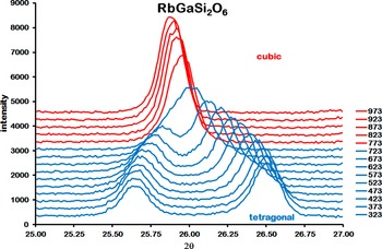
The initial run 1 XRD data were collected over the range from 25 to 27 °2θ. These data showed the tetragonal (004) and (400) Bragg reflections for RbGaSi2O6 at room temperature. On heating, these two Bragg reflections get closer together. By 773 K, these two reflections have merged into a single peak, suggesting a transition to a cubic structure (see Figure 1).
High-temperature XRD data for RbGaSi2O6 over the range of 25–27°2θ, measured from 323 to 973 K.

The subsequent run 2 XRD data were collected as 30-minute scans over the range from 15 to 100 °2θ at 298 K, 623 K, and in 10 K steps from 673 to 823 K before a 10-hour scan at 873 K.
These run 2 powder diffraction data were analyzed using HighScore Plus 4.7 (PANalytical, 2017b) and the ICDD Powder Diffraction File (Kabekkodu et al., Reference Kabekkodu, Dosen and Blanton2024). Analysis of the 298 K powder diffraction data for RbGaSi2O6 showed that this sample consisted of two phases. The main phase was I41/a tetragonal RbGaSi2O6 PDF# 00-037-0350 with C2/m monoclinic Ga2O3 PDF# 00-043-1012 as an impurity phase. Rietveld refinements were done using FULLPROF (Rodríguez-Carvajal, Reference Rodríguez-Carvajal1993) for XRD data collected up to 823 K. GSAS-II (Toby and Von Dreele, Reference Toby and Von Dreele2013) was used for Rietveld refinements on the 873 K data. Backgrounds were fitted by linear interpolation between a set of background points with refinable heights. The Thompson–Cox–Hastings pseudo-Voigt function (van Laar and Yelon, Reference van Laar and Yelon1984), convoluted with asymmetry due to axial divergence (Finger et al., Reference Finger, Cox and Jephcoat1994), was used to model the profile shape.
The crystal structure of RbGaSi2O6 was refined using the I41/a structure of RbGaSi2O6 (Bell and Stone, Reference Bell and Stone2021) as the starting model. In this crystal structure, all atoms were located on the I41/a 16f Wyckoff general position. There is one 16f position for Rb, three 16f positions for T-sites (with disordered occupancies of one-third Ga and two-thirds Si, T-site occupancies were not refined), and six 16f positions for O. The isotropic temperature factors of the T-site atoms Si and Ga were constrained to be the same on each T-site but were allowed to vary between different T-sites. All isotropic temperature factors for the six O sites were constrained to have the same value. The T–O interatomic distances were soft constrained to be 1.68 ± 0.02 Å (average bond distance for tetrahedral Si–O and Ga–O), assuming complete T-site disorder (1/3Ga:2/3Si on each T-site), as it was not possible to refine chemically sensible T-site occupancies. Rietveld refinements in non-cubic leucite structures without soft interatomic distance constraints tend to give unrealistic interatomic T–O distances. The crystal structure of Ga2O3 (da Silva et al., Reference da Silva, Sosman, Yokaichiya, Mazzocchi, Parente, Mestnik-Filho, Henry and Bordallo2012) was used to fit the impurity phase; only lattice parameters were refined.
The refined structural parameters were used as a starting model for the 623 K data; subsequent refinements were done with the refined parameters used as a starting model for the next temperature up. As the temperature increased, the a and c lattice parameters moved closer together. At 733 K, the a and c lattice parameters were so close that it was possible to refine the crystal structure for RbGaSi2O6 with an Ia
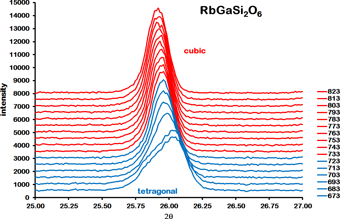
![]() d cubic structure that was isostructural with pollucite (CsAlSi2O6). In this cubic structure, Rb replaced Cs on the extra-framework cation site and Ga replaced Al on the disordered T-site. This cubic structure was retained up to 873 K. Figure 2 shows the run 2 XRD data over the range from 25 to 27 °2θ heating from 673 to 823 K. This shows how a closely overlapped double peak for the tetragonal (004) and (400) Bragg reflections merge to form a single cubic (400) Bragg reflection at 733 K. Figure 3 shows a Rietveld difference plot for RbGaSi2O6 at 873 K; this difference plot shows Bragg reflections for cubic RbGaSi2O6 and Ga2O3 impurity. Note that there are also two weak unassigned Bragg reflections at 27.15 and 27.55 °2θ in the 873 K difference plot.
d cubic structure that was isostructural with pollucite (CsAlSi2O6). In this cubic structure, Rb replaced Cs on the extra-framework cation site and Ga replaced Al on the disordered T-site. This cubic structure was retained up to 873 K. Figure 2 shows the run 2 XRD data over the range from 25 to 27 °2θ heating from 673 to 823 K. This shows how a closely overlapped double peak for the tetragonal (004) and (400) Bragg reflections merge to form a single cubic (400) Bragg reflection at 733 K. Figure 3 shows a Rietveld difference plot for RbGaSi2O6 at 873 K; this difference plot shows Bragg reflections for cubic RbGaSi2O6 and Ga2O3 impurity. Note that there are also two weak unassigned Bragg reflections at 27.15 and 27.55 °2θ in the 873 K difference plot.
High-temperature XRD data for RbGaSi2O6 over the range of 25–27°2θ, measured from 673 to 823 K.

Rietveld difference plot for RbGaSi2O6 from data collected at 873 K. The red circles represent the observed data points, the blue line represents the calculated data points, and the green line represents the difference curve. The upper line of black crosses represents the positions of Bragg reflections for RbGaSi2O6, whereas the lower line of black crosses represents the positions of Bragg reflections for Ga2O3 impurity. R-factors for this refinement were Rp = 2.044%, R wp = 3.282%, R exp = 1.013%, and χ 2 = 3.24.

VESTA (Momma and Izumi, Reference Momma and Izumi2011) was used to plot crystal structures. Figure 4a,b, respectively, shows the crystal structure plots for RbGaSi2O6 at 873 and 298 K (Bell and Stone, Reference Bell and Stone2021).
VESTA structure plots for RbGaSi2O6. Extra-framework Rb+ cations are shown in pink, disordered (Si/Ga)O4 tetrahedra in light green, and O2− anions in red. Panel (a) shows the Ia
![]() d cubic 873 K crystal structure, viewed down [111], showing the channel for extra-framework cations. Panel (b) shows the I41/a tetragonal 298 K crystal structure, viewed down [1-11], showing the channel for extra-framework cations (Bell and Stone, Reference Bell and Stone2021).
d cubic 873 K crystal structure, viewed down [111], showing the channel for extra-framework cations. Panel (b) shows the I41/a tetragonal 298 K crystal structure, viewed down [1-11], showing the channel for extra-framework cations (Bell and Stone, Reference Bell and Stone2021).

III. RESULTS AND DISCUSSION
Crystal structures have been refined for the RbGaSi2O6 leucite analogue from X-ray powder diffraction data over the temperature range from 298 to 873 K. All refined structures have disordered T-site cations. RbGaSi2O6 is isostructural with I4
1/a tetragonal leucite (KAlSi2O6; Mazzi et al., Reference Mazzi, Galli and Gottardi1976) from 298 to 723 K. At 733 K, there is a phase transition, and the crystal structure is then isostructural with Ia
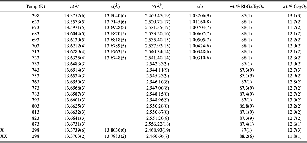
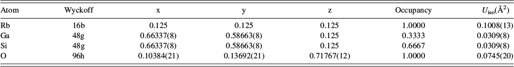
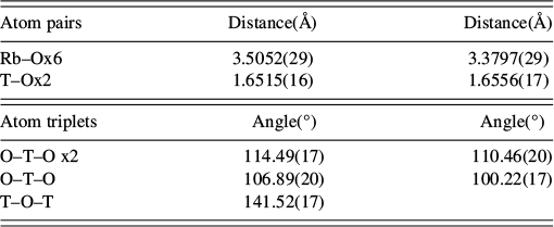
![]() d cubic pollucite (CsAlSi2O6; Yanase et al., Reference Yanase, Kobayashi, Shibasaki and Mitamura1997). Table I shows how the refined lattice parameters for RbGaSi2O6 vary with temperature, and Figures 5 and 6 show how the lattice parameters and unit cell volume for RbGaSi2O6 vary with temperature. Table II shows the refined coordinates, and Table III shows the refined interatomic distances and angles for RbGaSi2O6 at 873 K.
d cubic pollucite (CsAlSi2O6; Yanase et al., Reference Yanase, Kobayashi, Shibasaki and Mitamura1997). Table I shows how the refined lattice parameters for RbGaSi2O6 vary with temperature, and Figures 5 and 6 show how the lattice parameters and unit cell volume for RbGaSi2O6 vary with temperature. Table II shows the refined coordinates, and Table III shows the refined interatomic distances and angles for RbGaSi2O6 at 873 K.
Variation of RbGaSi2O6 lattice parameters and phase proportions on heating.

298–723 K: I41/a tetragonal; 733–873 K: Ia![]() d cubic. “X” denotes data collected in the furnace after heating, and “XX” denotes ambient-temperature data not measured in the furnace (Bell and Stone, Reference Bell and Stone2021).
d cubic. “X” denotes data collected in the furnace after heating, and “XX” denotes ambient-temperature data not measured in the furnace (Bell and Stone, Reference Bell and Stone2021).
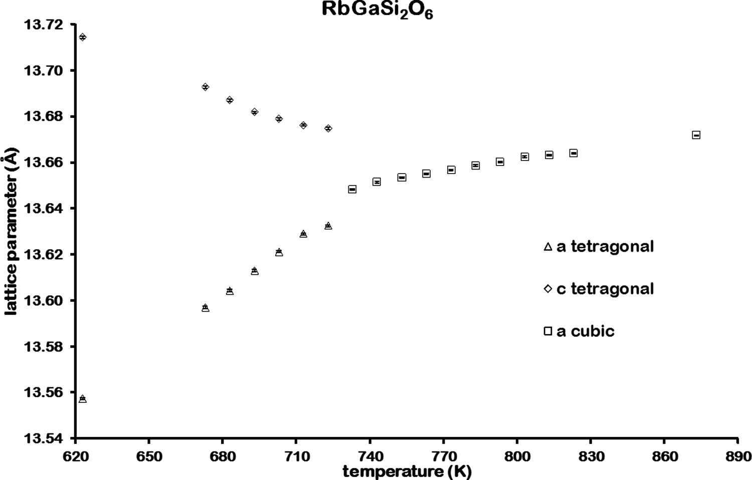
Variation of lattice parameters for RbGaSi2O6 from 623 to 873 K.

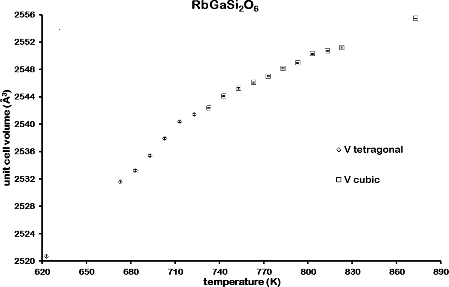
Variation of unit cell volume for RbGaSi2O6 from 623 to 873 K.

Refined cubic coordinates for RbGaSi2O6 Ia
![]() d at 873 K.
d at 873 K.

Refined distances and angles for RbGaSi2O6 Ia
![]() d at 873 K.
d at 873 K.

“T” denotes the disordered Ga/Si site. Tetrahedral angle variance [σ
2, deg2] for Ia
![]() d RbGaSi2O6 at 873 K = 28.92. σ
2 = Σ(θ − 109.47)2/5 (Robinson et al., Reference Robinson, Gibbs and Ribbe1971), where θ is the O–T–O tetrahedral angle.
d RbGaSi2O6 at 873 K = 28.92. σ
2 = Σ(θ − 109.47)2/5 (Robinson et al., Reference Robinson, Gibbs and Ribbe1971), where θ is the O–T–O tetrahedral angle.
Figure 6 shows how the unit cell volume for RbGaSi2O6 varies with temperature; there is no step change in unit cell volume at the phase transition temperature at 733 K. This suggests that RbGaSi2O6 has a second-order I4
1/a tetragonal to Ia
![]() d cubic phase transition. KGaSi2O6 also has an I4
1/a tetragonal to Ia
d cubic phase transition. KGaSi2O6 also has an I4
1/a tetragonal to Ia
![]() d cubic phase transition (Bell and Henderson, Reference Bell and Henderson2020). However, this transition is different from that of RbGaSi2O6 in that there is a two-phase region in this transition. Bragg reflections for both cubic and tetragonal KGaSi2O6 are present over the temperature range from 673 to 970 K; no similar two-phase region is observed for RbGaSi2O6. There is also a step change in unit cell volume from tetragonal to cubic for KGaSi2O6, suggesting a first-order phase transition.
d cubic phase transition (Bell and Henderson, Reference Bell and Henderson2020). However, this transition is different from that of RbGaSi2O6 in that there is a two-phase region in this transition. Bragg reflections for both cubic and tetragonal KGaSi2O6 are present over the temperature range from 673 to 970 K; no similar two-phase region is observed for RbGaSi2O6. There is also a step change in unit cell volume from tetragonal to cubic for KGaSi2O6, suggesting a first-order phase transition.
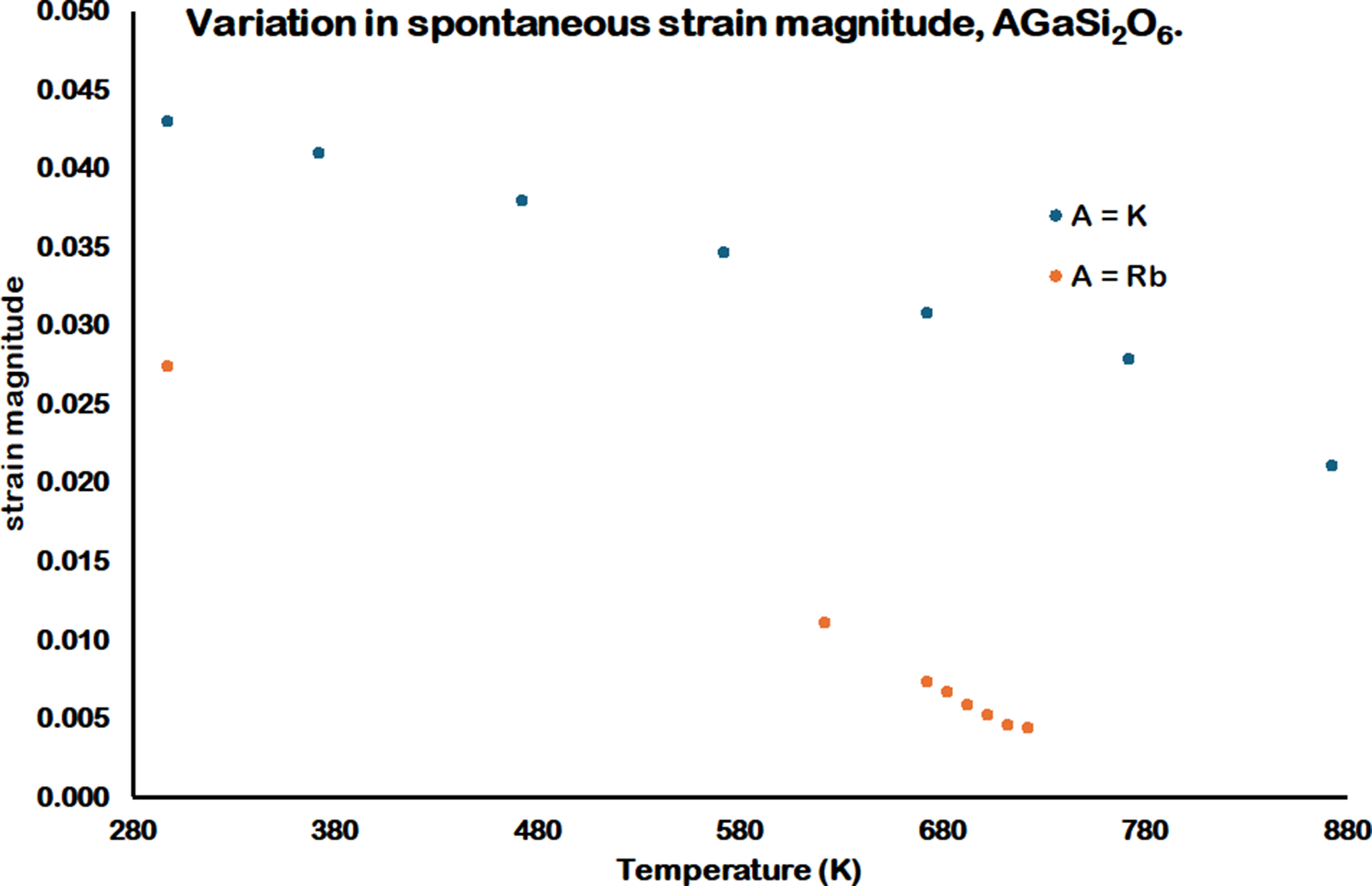
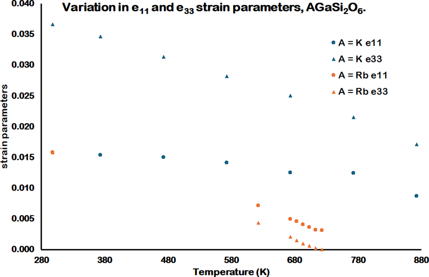
The equations of Carpenter (Carpenter et al., Reference Carpenter, Salje and Graeme-Barber1998) have been used to determine the spontaneous strain parameters for RbGaSi2O6 and KGaSi2O6 below the tetragonal to cubic phase transition temperatures. Figure 7 shows the variation of the spontaneous strain, and Figure 8 shows the variation of the e 11 and e 33 strain parameters for RbGaSi2O6 and KGaSi2O6. These figures show that the magnitudes of the strain parameters are greater for KGaSi2O6 compared with RbGaSi2O6. This may be due to the smaller K+ extra-framework cation causing a greater degree of framework collapse (Taylor and Henderson, Reference Taylor and Henderson1968) compared with the larger Rb+ extra-framework cation. Consequently, the tetragonal crystal structure for KGaSi2O6 would show a greater degree of strain compared with RbGaSi2O6.
Variation spontaneous strain parameters for tetragonal AGaSi2O6 (A = K, Rb) from 298 to 873 K.

Variation in e 11 and e 33 strain parameters for tetragonal AGaSi2O6 (A = K, Rb) from 298 to 873 K. Note that the A = K e 33 and the A = Rb e 11 and e 33 strain parameters at 298 K cannot be resolved in this figure, as these parameters have similar values.

Qualitative EDX mapping of the RbGaSi2O6 sample: (a) gallium map; (b) rubidium map; (c) oxygen map; and (d) silicon map.

Ga2O3 is present as an impurity phase at all temperatures. Table I shows that the phase proportion of RbGaSi2O6 is constant within error limits over the temperature range. This indicates that there is no further reaction of impurity Ga2O3 over the temperature range. However, Table I shows that the Ga2O3 is present as an impurity phase at approximately 12 wt.%. Rietveld refinements were done using the I41/a tetragonal (leucite) and Ia
![]() d cubic (pollucite) crystal structures as starting models; this assumed that the T-sites were occupied by Si and Ga in a 2:1 ratio. The presence of a significant amount of Ga as an impurity means that this Si/Ga ratio may be greater than 2. However, if this Si/Ga ratio has become higher than 2, it has not got to the range where any leucite analogues are replaced by Ga-containing feldspar analogous to RbAlSi3O8 (Gasperin, Reference Gasperin1971), which has a C2/m monoclinic crystal structure.
d cubic (pollucite) crystal structures as starting models; this assumed that the T-sites were occupied by Si and Ga in a 2:1 ratio. The presence of a significant amount of Ga as an impurity means that this Si/Ga ratio may be greater than 2. However, if this Si/Ga ratio has become higher than 2, it has not got to the range where any leucite analogues are replaced by Ga-containing feldspar analogous to RbAlSi3O8 (Gasperin, Reference Gasperin1971), which has a C2/m monoclinic crystal structure.
To investigate the stoichiometry, specifically the Si/Ga ratio in this RbGaSi2O6 sample, SEM and EDS were used to analyze different areas of this sample.
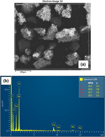
EDS mapping was used to investigate the spatial distribution of the constituent elements of the sample qualitatively (see Figure 9). From these maps, it is evident that in regions where the gallium content is high, there is a drop in silicon content. This is therefore consistent with there being an increased volume fraction of Ga2O3 in this region. Further investigation of the sample revealed inclusions of Ga2O3 in the RbGaSi2O6 matrix (see Figure 10a,b). Theoretically, for a volume fraction of 12% Ga2O3 in a matrix of 88% RbGaSi2O6, where both components are stoichiometric, we would expect a composition of 31.23 wt.% O, 28.20 wt.% Ga, 24.47 wt.% Rb, and 16.08 wt.% Si. A wide area EDX spectrum was acquired from an approximate area of 1 mm2; the averaged composition of this area is 32.5 wt.% O, 26.6 wt.% Ga, 22.7 wt.% Rb, and 18.2 wt.% Si. This is in close agreement with the XRD result (see Figure 11a,b). Additionally, a point spectrum (see Figure 10c) in the RbGaSi2O6 matrix gives a composition of 29.3 wt.% O, 21.5 wt.% Ga, 27.1 wt.% Rb, and 22.1 wt.% Si. This would suggest that the RbGaSi2O6 matrix has a Si/Ga ratio close to 2.
Scanning electron microscopy image of a Ga2O3 inclusion: (a) secondary electron image; (b) energy dispersive spectroscopy (EDS) spectrum obtained from a Ga2O3 inclusion; and (c) EDS spectrum recorded from the matrix.

Scanning electron microscopy image acquired from an approximate area of 1 mm2: (a) secondary electron image and (b) energy dispersive spectroscopy spectrum.

Figure 4a,b (873 and 298 K; Bell and Stone, Reference Bell and Stone2021), respectively, shows the VESTA crystal structure plots for RbGaSi2O6. Note that Figure 4b shows that the tetragonal crystal structure has a slightly collapsed silicate framework structure compared with the cubic structure shown in Figure 4a.
IV. CONCLUSIONS
RbGaSi2O6 leucite analogue has a high-temperature phase transition from I41/a tetragonal (KAlSi2O6 leucite structure) to Ia
![]() d cubic (CsAlSi2O6 pollucite structure) at 733 K. This transition is reversible on cooling to room temperature.
d cubic (CsAlSi2O6 pollucite structure) at 733 K. This transition is reversible on cooling to room temperature.
DEPOSITED DATA
CIF files containing information on the 873 K crystal structure, interatomic distances and angles, and powder diffraction data for RbGaSi2O6 synthetic leucite analogue were deposited with the ICDD. These data can be requested from ICDD at info@icdd.com.
ACKNOWLEDGEMENTS
We acknowledge the use of the EPSRC-funded National Chemical Database Service, hosted by the Royal Society of Chemistry.


 Open access