

1. Introduction
The most challenging problem for the realization of high power GaN/InGaN/AlGaN lasers is the very high density of threading dislocations present in epitaxial layers and device structures Reference Nakamura[1]. These dislocations result from the lattice mismatch between sapphire or SiC substrates and nitride overlayers. Due to the advancements in epitaxial technology, in particular in lateral overgrowth techniques (ELOG, PENDEO, FIELO) Reference Zheleva, Nam, Ashmawi, Griffin and Davis[2], it has been possible to lower the density of dislocations to the level of roughly 107 cm−2. However, in such structures, in spite of their sophistication, one can still find tens or hundreds of dislocations in the active area of typical laser diodes. The situation becomes even worse in case of wide stripe laser diodes. These lasers suffer from an increased number of defects within their active layer and, moreover, are difficult to manufacture because the standard ELOG techniques leave only narrow regions on the wafer with lowered dislocation density. These regions are usually too narrow to contain broader (15-50 μm) stripes. Since the lifetime of GaN/InGaN/AlGaN lasers is directly related to the density of dislocations in the material Reference Takeya[3], the only way to produce fully reliable devices is to a use qualitatively better substrate material. A new path was paved recently by a Japanese company - Sumitomo, which succeeded in producing high quality GaN layers characterized by a dislocation density of the order of 105−106cm−2. By using their proprietary FIELO-like technology called “DEEP” (dislocation elimination method), they are able to produce much larger low-dislocation-density areas on their wafers. Sony and Sanyo are currently manufacturing prototypes of high power laser diodes on this type of substrate (see Ref. Reference Takeya, Tojyo, Asano, Ikeda, Mizuno, Matsumoto, Goto, Yabuki, Uchida and Ikeda[4] as an example). However, the “DEEP” method is very laborious and requires multiple regrowth and processing steps while still not eliminating completely the inhomogeneous strain distribution. Thus it is still very tempting to find a simpler and less laborious method of substrate preparation.
In this paper, we will demonstrate the applicability of single GaN crystals, obtained from high-pressure, high-temperature synthesis, as substrates for the growth of low dislocation density laser diode structures. The first report on laser emission from this type of structure was published earlier Reference Grzegory, Bockowski, Krukowski, Lucznik, Wroblewski, Weyher, Leszczynski, Prystawko, Czernecki, Lehnert, Nowak, Perlin, Teisseyre, Purgal, Krupczynski, Suski, Dmowski, Litwin-Staszewska, Skierbiszewski, Lepkowski and Porowski[5], and since then the development of these devices has been directed towards the construction of high power LDs.
2. Substrates
The GaN crystals grown by the High Nitrogen Pressure Solution Reference Grzegory[6] method are of wurzite structure, mainly in the form of hexagonal platelets. The large hexagonal surfaces correspond to {0001} polar crystallographic planes. The side faces of the crystals are mainly the polar {10
Processed laser structure on GaN single crystal substrate prior to cleavage and device separation.

3. Epitaxy
We grow our GaN/AlGaN/InGaN laser structures in a home-made vertical flow MOVPE reactor using TMGa, TEGa, TMAl, TMIn, CP2Mg, SiH4 and ammonia as precursors Reference Prystawko, Czernecki, Leszczynski, Perlin, Wisniewski, Dmowski, Teisseyre, Suski, Grzegory, Bockowski, Nowak and Porowski[7]. The growth is controlled in-situ by reflectometry. During the homoepitaxial growth of nitride layers on GaN substrate, there is no need to grow a low-temperature nucleation layer. After first ammonia annealing step, GaN is grown immediately at 1050 °C on the Ga-face of the GaN crystal. The further growth of InGaN and AlGaN layers does not deviate too much from the recipes known from analoguous hetero-epitaxial processes. In some cases the upper p-type GaN contact layer was deposited using a RF-plasma, MBE VG SEMICON 90 machine. The quality of epitaxial structure was tested by a selective etching method Reference Kamler, Weyher, Grzegory, Jezierska and Wosinski[8]. An example of such a study is shown in Figure 2, revealing an etch pit density of 3·105 cm−2. This result is very satisfactory when compared to ELO epitaxy on sapphire substrates (recent reports indicate similar density of dislocation in the lasers structures manufactured by Sony with Sumitomo quasi-bulk GaN substrates) Reference Takeya, Tojyo, Asano, Ikeda, Mizuno, Matsumoto, Goto, Yabuki, Uchida and Ikeda[4] Reference Takeya, Tojyo, Asano, Ikeda, Mizuno, Matsumoto, Goto, Yabuki, Uchida and Ikeda[4], though it clearly demonstrates the appearance of new dislocations, probably at the lower AlGaN cladding interface.
SEM photograph of selectively etched laser structure. The etch pit density on this photograph is around 5·105cm−2. The stripe width is 15μm, T = 300 K.

4. Device processing
The devices were processed as ridge-waveguide, oxide-isolated lasers. The mesa structure was etched out in the wafer to a depth of 0.3 μm (roughly to the middle of the upper cladding layer), see Figure 3. The laser structure was then isolated by the e-beam deposition of a 0.2 μm layer of SiOx. The stripe width is 15 μm and the resonator length 500 μm. The reflectivity of the cleaved mirrors was increased to 50% by coating them with two pairs of quarter-wavelength layers of SiO2/ZrO2. The oxidized Ni/Au ohmic contacts, of typical contact resistance 1·10−4 Ω ·cm2, were deposited on the top surface of the device, while Ti/Au contacts were deposited on the backside of the highly conducting n-GaN crystal. Maximum hole concentration in the p-GaN layers was close to 3·1017cm−3 (mobility ≈3 cm2V/s) which corresponds to the resistivity of 5·Ωcm.
Details of the laser structure.

5. Device characterization
The electrical and optical characterization were performed using a custom-made pulsed current source which provides 30 to 200 ns current pulses with a repetition rate from 1 to 100 kHz. For optical power calibration we used a Newport 1815 C optical power meter equipped with 818 UV head. The pulse length of the optical signal was measured with a Tektronix TDS 3034 B digital oscilloscope with a high speed silicon PIN photodetector. The spectra were measured using a miniature Ocean Optics SD 2000 spectrometer or an Acton SpectraPro 500i spectrometer.
By changing the indium fraction in InGaN quantum wells, we were able to change the emission wavelength from 390 to 430 nm. Examples of emission spectra are shown in Figure 4. In the present paper, we will focus on devices operating at a wavelength close to 415 nm, though the characteristics of devices operating at shorter wavelength are very similar.
Emission wavelength of various laser diodes grown on bulk GaN substrates.
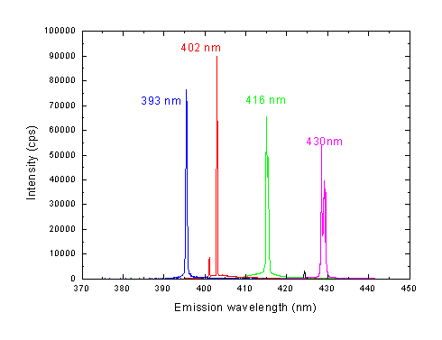
Figure 5 shows the basic electrical and optical characteristics of our lasers, all measured under pulsed current conditions (30 ns pulse length, 10 kHz repetition, room temperature). The emission wavelengths of the lasers are between 415 and 420 nm. The threshold currents for these lasers are between 500 and 800 mA, depending on the particular device, while the threshold voltage ranges from 7.5 to 9 V. These values correspond to current densities of 6.6−10 kA/cm2. This current density is still a factor of two higher than for devices manufactured by Nichia and Sony Reference Takeya, Tojyo, Asano, Ikeda, Mizuno, Matsumoto, Goto, Yabuki, Uchida and Ikeda[4] Reference Mukai, Nagahama, Yanamoto and Sano[9]. We attribute this fact to excessive carrier overflow. The slope efficiency of the device is in the range of 0.25−0.3 W/A per facet (0.5-0.6 W/A for total emission) for the current range 0-3 A. For higher currents the efficiency slightly decreases. The maximum optical power per mirror was 1.3 W (very recent results give the maximum peak power of 1.9 W per facet which means 3.8 W of total optical power, see the red curve in Figure 5) and was limited by the current range of the pulse power supply used in the experiment. Because of the symmetric coating, the total optical power can be stated to exceed 2.6 W (3.8 W in the newest results), which makes this probably the highest pulsed optical power reported for nitride lasers.
Current -voltage and current-light characteristics of a high-power, pulsed current operated laser diode. Red curve shows record-high current-light characteristic measured for another device.
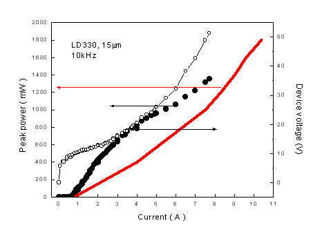
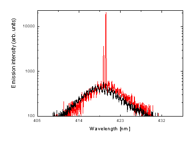
Figure 6 shows spectra of emitted light measured at different currents close to the lasing threshold. The observed mode separation (5 Å) is almost 10 times larger than predicted for longitudinal modes which is a kind of a fingerprint of nitride lasers. Measurements of the temperature dependence of the threshold current (see Figure 7) give a value of T0 in the range of 94-120 K. Here T0 represents the parameter describing the temperature dependence of the threshold current according to the Equation (1) below:

Just below and just above threshold spectra of laser diode measured at room temperature under pulsed current condition (30 ns, 10 kHz). Threshold current ≈400 mA.
Temperature shift of the threshold current. The determined T0 parameter is equal to 94K.
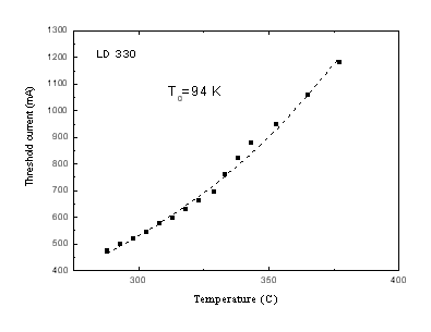
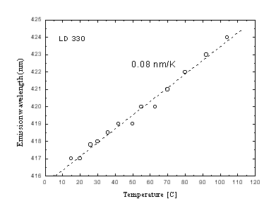
T0 represents here all types of thermally activated processes, including nonradiative recombination and, what seems to be more important, carrier overflow. This latter effect can be controlled by the proper design of AlGaN blocking layer. Reference Takeya, Tojyo, Asano, Ikeda, Mizuno, Matsumoto, Goto, Yabuki, Uchida and Ikeda[4] Reference Hansen, Piprek, Pattison, Speck, Nakamura and DenBaars[10] It has already been demonstrated that both composition and exact location of electron blocking layer have a direct impact on the T0 value Reference Hansen, Piprek, Pattison, Speck, Nakamura and DenBaars[10]. The relatively low value of T0 as compared to the best literature values (T0 = 235 K)9 indicates the need for the further optimization of the electron blocking layer and the quantum well system. The temperature shift of the emission, illustrated in Figure 8, was found to be 0.08 nm/K (0.6 meV/K). This shift agrees well with the change of GaN energy gap Reference Teisseyre, Perlin, Suski, Grzegory, Porowski, Jun, Pietraszko and Moustakas[11] for the studied temperature range.
Temperature shift of the emission line.
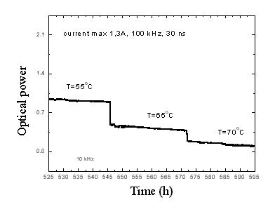
The devices were lifetested under constant amplitude current conditions and variable temperature. An example of such a procedure is shown in Figure 9. By using variable temperature accelerated tests, a lifetime of up to 12 000 h was predicted at the following conditions: current 1 A, frequency 100 kHz, pulse length 30 ns. The activation energy of the degradation processes was estimated to be 0.32 eV.
Constant amplitude current, variable temperature, degradation test of pulse current operated laser diode.
Our wide-stripe lasers have still rather high electrical threshold power, always above 3.2 W. So far, within our mounting and packaging technical capabilities, we were unable to efficiently dissipate such a high amount of heat. The maximum duration of the light pulse was not longer than 5 μs, after this time the device was overheated and the lasing stopped. We believe that with a further reduction of operating voltage and current and with improved packaging, stable CW operation should be reached soon.
In conclusion, we have demonstrated the applicability of bulk GaN crystals as substrates for the fabrication of high-power laser diodes. The typical density of dislocations in such structures is in the range of 105 cm−2. The total emitted power exceeds 3.9 W in 30 ns pulses, which is the best value ever reported
Acknowledgments
The work was supported by the Polish Government program “The development of blue optoelectronics”, project number 2700/C.T11-8/2000 The work of G. Franssen was supported by the European Commission, Grant "Support for centers of Excellence" No. ICA1-CT-2000-70005.


