





1. Introduction
Semiconductors represent one of the most important technological innovations of modern times. They are used in, for instance, consumer electronics, industrial automation applications, and data storage devices, and the growing need for digitalization and electrification is expected to double the semiconductor market from 2023 to 2030 (Mahindroo et al., Reference Mahindroo, Suryanarayanan, de Jong, Kakarwada and Patel2025). Additionally, climate and environmental crises urge the semiconductor industry to reform its current practices, because the sector's rapid growth has resulted in substantial environmental impacts (Wang et al., Reference Wang, Huang, Chen, Chen, Cai and Wu2023). Driven by global geopolitical tensions, legislative efforts around critical raw materials (CRMs) like tungsten, titanium, and cerium have also intensified, with the EU and the USA leading the way (European Commission, 2023; Hale et al., Reference Hale, Ali, Christman, Bleischwitz, Svobodova, Primmer, Moutinho and Kulczycka2025; Regulation (EU) 2024/1252, 2024). The Critical Raw Materials Act by the EU aims at ensuring both secure and sustainable supply of these materials (Hale et al., Reference Hale, Ali, Christman, Bleischwitz, Svobodova, Primmer, Moutinho and Kulczycka2025). The Act emphasizes developing recycling technologies for CRMs for their circular supply and companies’ responsibility to carry out risk assessments about their supply chains. Accordingly, the semiconductor industry seeks to improve its resilience in order to avoid supply chain disruptions and to strengthen its global competitiveness (CHIPS and Science Act of 2022, 2022; Regulation (EU) 2023/1781, 2023). In this study, CRMs are defined by the European Commission, based on their economic importance and supply risk, which vary regionally. Additionally, strategic raw materials (SRMs) are regarded as the most crucial for strategic technologies, e.g., in decarbonization, digital, defence, and aerospace applications (Regulation (EU) 2024/1252, 2024).
The circular economy can reduce environmental impacts while mitigating risks linked to the criticality of raw materials. By decreasing material use and increasing recovery for recycling, the so-called R-strategies can help lower greenhouse gas (GHG) emissions and other environmental impacts by limiting the need for virgin material extraction (European Commission, 2020). The 9R framework, which is often used to describe circular strategies, refers to strategies aiming at narrowing, slowing, and closing material and energy loops across product's life cycle, including activities like reduce, reuse, repurpose, and recycle (Kirchherr et al., Reference Kirchherr, Reike and Hekkert2017). Within the 9R framework, recovery for recycling is considered a lower-order R-strategy, which, as such, is not enough for reaching circular economy or addressing the root causes of environmental impacts (Ellen MacArthur Foundation, 2013; Kirchherr et al., Reference Kirchherr, Reike and Hekkert2017). However, in semiconductor manufacturing, recovery is relevant for improving self-sufficiency by reducing the reliance on virgin materials whose supply is critical (Ellen MacArthur Foundation, 2025; Kirchherr et al., Reference Kirchherr, Reike and Hekkert2017). There is potential for the recovery of CRMs, since as much as 99% of CRMs applied during wafer processing, e.g. thin film deposition, are not present in the processed wafer (Vauche et al., Reference Vauche, Guillemaud, Lopes Barbosa and Di Cioccio2024). However, potential environmental impacts of circular practices, such as recovery of CRMs for recycling, have not yet drawn much attention in the scientific literature.
This study consists of two literature reviews and one case study. Firstly, a review of sustainability reports of global semiconductor manufacturers is conducted to obtain an overview of the recovered CRMs and other materials, which are assessed against companies’ circularity goals. Secondly, results from a scoping literature review focusing on existing solutions for recovering CRMs and precious metals, such as silver, gold, and platinum, in the semiconductor industry are presented. Finally, a life cycle assessment (LCA) case study examines membrane technology as a potential recovery method, demonstrating its potential impacts from climate and criticality perspectives.
The LCA case study concentrates on a chemical-mechanical polishing (CMP) process where a wafer is polished to remove any excess material and ensure that its surface is smooth. Besides deionized water and chemicals, CMP slurry contains abrasive particles, like ceria (CeO2), silica (SiO2), or alumina (Al2O3), which play a crucial role in the CMP process, enabling simultaneously mechanical polishing and chemical reactions on the wafer surface. The case study compares a typical process where spent slurry is disposed of with wastewater to a process where ceria is recovered from the slurry for recycling. LCA approach is used to quantify the recovery solution's climate impact, which is a key impact category for the semiconductor industry (e.g. by Kuo et al. (Reference Kuo, Kuo and Chen2022) and Vauche et al. (Reference Vauche, Guillemaud, Lopes Barbosa and Di Cioccio2024)).
In addition to climate impacts, implementation of circularity indicators was considered in this context as they can be beneficial to measure and monitor the alignment with the principles of circular economy (WBCSD, 2023). However, these mass-based indicators were deemed unsuitable here as the recycled content is minimal. The ‘circular outflow’ of the Circular Transition Indicator would be 0.007%, which does not reflect the critical role of ceria in this context. Instead, raw material criticality assessment (CA) was conducted using the indicators supply risk (SRm), economic importance (EIm), and material criticality (MC) since circularity links strongly to criticality through efficient resource use, supply chain resilience, and economic aspects (Hackenhaar et al., Reference Hackenhaar, Moraga, Thomassen, Taelman, Bachmann and Dewulf2025). The applied CA method builds upon the European Commission's Criticality Assessment method (2023).
2. Recycling of CRMs in the semiconductor industry
2.1. Circularity goals and material recovery practices in the semiconductor industry
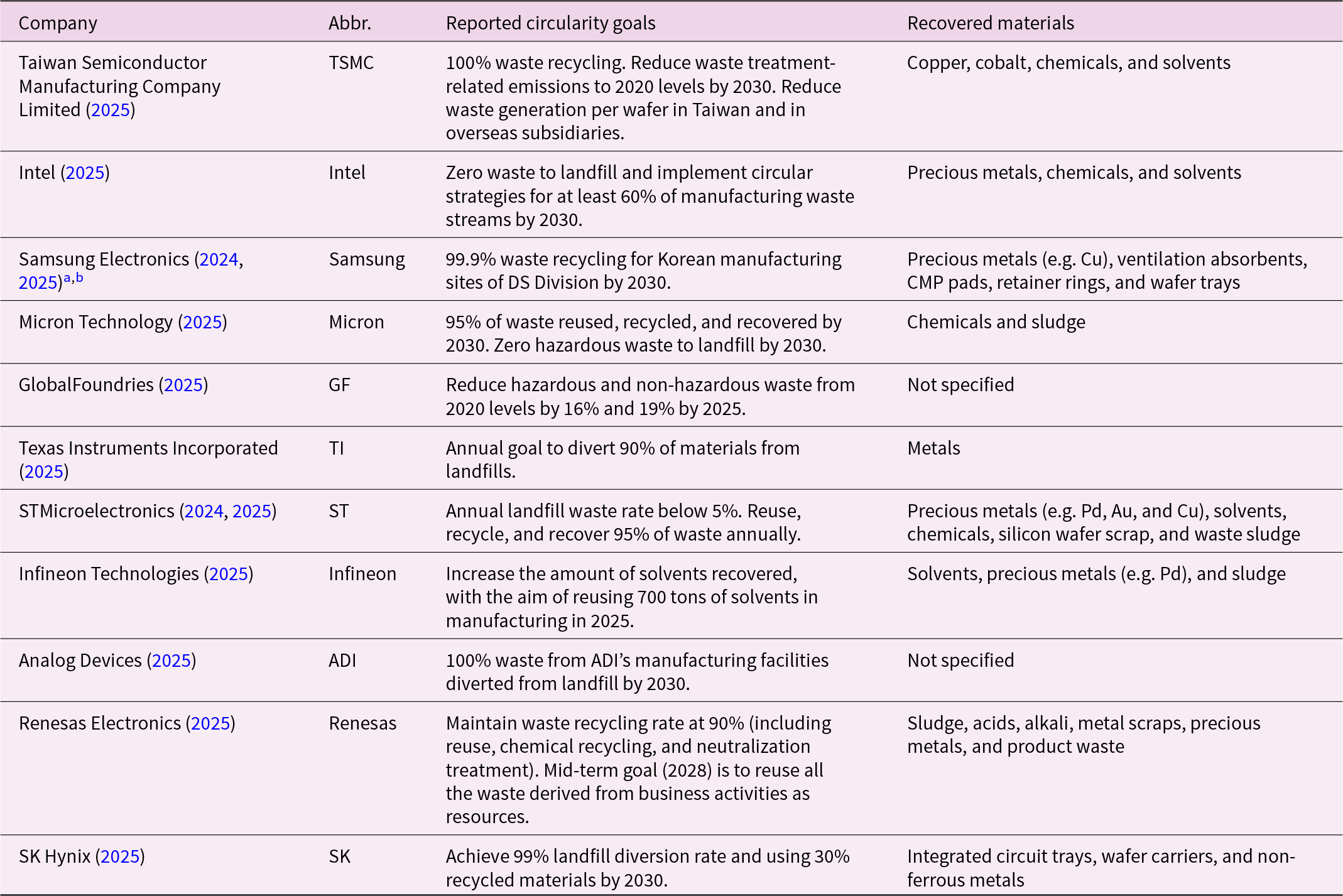
To obtain an overview of the current state of material recovery in semiconductor manufacturing processes, the corporate sustainability reports of 11 foundry or integrated device manufacturer companies were reviewed. The review was non-exhaustive in nature. In addition to representing large to mid-size global companies located in Taiwan, South Korea, Japan, Switzerland, Germany, and the United States, the selected companies were required to have publicly available sustainability reports. For each company, the most recent sustainability report about the performance in 2024 was analysed. Due to the limited number of references to metal recovery from manufacturing processes, the scope of the review was expanded to include other recovered materials. Furthermore, circularity-related goals reported by the companies were examined to determine whether there was a connection between stated targets and material recovery activities. Table 1 shows the studied companies and their abbreviations, along with the key aspects concerning circularity goals and material recovery as stated within the analysed reports.
Summary of circularity goals and recovered materials reported by the companies studied

Table 1 Long description
The table compares semiconductor companies’ reported circularity goals and the types of materials they say they recover. Many set high diversion or recycling targets for 2030, including TSMC at full waste recycling, Intel at zero waste to landfill with circular strategies for most waste streams, Samsung’s DS division at near-total recycling in Korea, Micron at high reuse and recycling plus zero hazardous landfill, and ADI at full diversion from landfill. STMicroelectronics combines a low landfill waste rate with a high annual reuse, recycle, and recovery target, while SK hynix targets very high landfill diversion and also a recycled-materials use target. Some goals focus on reductions from a baseline year, such as GlobalFoundries and TSMC’s waste-related emissions and waste-per-wafer reductions. Recovered materials commonly include solvents, chemicals, precious metals, and sludge; several also cite copper or other metals, and Samsung and SK hynix list specific manufacturing items like trays, pads, rings, and carriers. Two companies, GlobalFoundries and ADI, do not specify recovered materials. Interpret comparisons cautiously because goals vary in scope, geography, and definitions, and Samsung’s entry reflects only one division rather than the whole company.
a Only the DS Division was considered for Samsung since it consists of business units that are responsible for producing and selling semiconductor components.
b For the recovered materials, also the sustainability report of 2023 performance was considered, since it elaborated on the recycling of precious metals.
Within the studied reports, the level of detail differs largely according to the recovered materials and their targeted use, with ADI and GF being the only ones not stating anything about materials recovered. ST shares, in greater detail, their process of recovering precious metals, such as copper, palladium, silver, and gold. They have partnered with an external company specializing in the recovery of precious metals through several thermal, chemical, and electrochemical processes and have achieved a recovery rate up to 99%. The resulting recycled materials are said to be of high quality, with similar characteristics to virgin materials, so that they can be reused in the semiconductor industry. Further examples of material recovery are silicon wafer scrap and waste sludge, which are used in aluminium production and as secondary raw materials. TSMC classifies liquid waste into 38 different types, for which there are 13 types of waste treatment available, so that finally 8 different products can be recycled internally or externally. Although the focus is on chemicals and solvents, such as ammonium sulphate and isopropanol, TSMC recovers also copper and cobalt from effluents. SK has initiatives to convert waste into resources and has a list of items, including integrated circuit trays, wafer carriers, and non-ferrous metals, that have been approved as circular resources by the Ministry of Environment in South Korea.
Infineon recovers precious metals, such as palladium, from silicon sludge waste, although in some cases the sludge itself can be recycled and used in cement kilns. On top of that, they recover chemicals from production processes, like etching and cleaning. Intel and Renesas recover precious metals for recycling without specifying which metals. Samsung states recovering precious metals, like copper, from wafer polishing consumables containing hazardous materials, whereas according to Renesas, the waste stream for metal recovery includes scrap wafers from the production. Intel and Renesas both additionally recover chemicals and solvents, while Renesas also recovers waste sludge, metal scrap, and product waste. Samsung's recovery activities include also ventilation absorbents, CMP pads and retainer rings, and wafer trays for regeneration. TI reports recovering metals from solids, liquids, scrap wafers, and other materials, without stating which metals are targeted. Micron distillates chemicals, e.g. isopropyl alcohol, for reuse and pursues sludge recycling. Although material recycling in the manufacturing processes demonstrates commitment to circular economy, it is not necessarily apparent from the overall circularity goals of the studied companies. When it comes to long-term circularity goals, TSMC, Intel, Micron, ADI, SK, and Samsung have announced tangible goals that they want to achieve by 2030 or 2050. GF, TI, Infineon, and ST, on the other hand, only have annual circularity goals. Renesas has mid-term goal until 2028, besides their annual goal. Moreover, TSMC, Intel, Samsung, Infineon, Renesas, and Micron have quantitative targets promoting circular thinking aimed at recycling and reusing materials both internally and by other industries. ADI, SK, and TI also have quantitative targets, but their approach is more waste management-focused than circularity-centred, as they aim to divert waste from landfills. GF works towards reducing its hazardous and non-hazardous waste amounts. Furthermore, SK has also set a target for the use of recycled materials in its products. Within the studied reports, there are no recycling goals specific to CRMs, and Infineon is the only company with a recovery target for a waste stream, specifically for solvents.
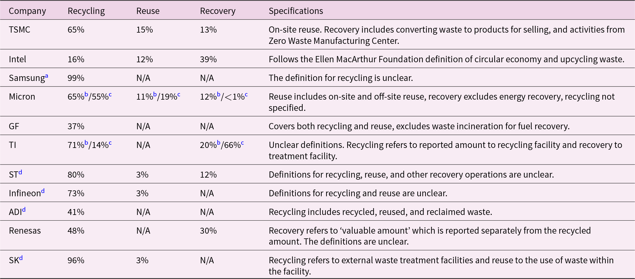
The level of detail reported on waste management and circularity practices varies significantly across companies. Table 2 shows recycling, reuse, and recovery rates from the total waste amounts as reported by the companies or calculated by authors when the rates were not readily available from the companies. Only TSMC, Intel, ST, and Micron disclose shares separately for recycling, reuse, and material recovery. GF, Samsung, and ADI report all activities under the recycling rate without detailing them further. The rates are similar for GF and ADI (37% and 41%, respectively), while Samsung has significantly higher rate with 99%, although Samsung's rate refers only to their Korean facilities, which could partly explain the high difference. For other companies that split the rates at least into two categories, recycling rates range between 41 and 80%, while SK reaches up to 96% and Intel only 16%. Reuse rates from their total annual waste generation are around 10–20% for TSMC, Intel, and Micron, but only around 3% for ST, Infineon, and SK. Intel and ADI's recovery rates are fairly high (39% and 30%, respectively) compared to those of TSMC (13%) and Micron (12% for non-hazardous, <1% for hazardous waste). Furthermore, TI recovers 20% of non-hazardous waste and 66% of hazardous waste. However, the recycling, reuse, and recovery rates should not be directly compared to each other since the definitions for recycling, reuse, and recovery were often unclear, and the scope of calculations might vary between companies.
Summary of annual rates for recycling, reuse, and recovery of total waste generation per company as collected from the studied sustainability reports
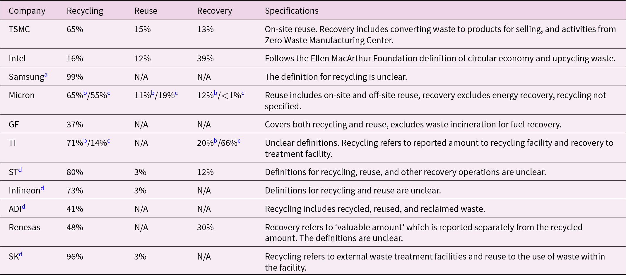
Table 2 Long description
The table compares company-reported annual shares of total waste that are recycled, reused, or recovered, with notes on how each company defines these terms. Only TSMC, Intel, Micron and ST report separately recycling, reuse and recovery rates while Samsung, GF and ADI only enclose recycling rates and the rest two of the afore mentioned categories. Recycling ranges from 16 percent at Intel to 99 percent at Samsung, though Samsung’s recycling definition is unclear. Several companies report high recycling with small reuse, including SK at 96 percent recycling and 3 percent reuse, and Infineon at 73 percent recycling and 3 percent reuse. TSMC reports 65 percent recycling, 15 percent reuse, and 13 percent recovery, with reuse described as on-site. Intel reports 16 percent recycling, 12 percent reuse, and the highest recovery at 39 percent, linked to circular economy and upcycling framing. Micron and TI provide separate figures for non-hazardous versus hazardous waste, showing large differences by waste type, such as TI shifting from 71 percent recycling and 20 percent recovery for non-hazardous to 14 percent recycling and 66 percent recovery for hazardous. Multiple entries note unclear or non-standard definitions, and some categories are not reported, so cross-company comparisons should be treated cautiously.
a Refers only to Korean facilities of the DS Division.
b Refers to the share from total non-hazardous waste.
c Refers to the share from total hazardous waste.
d Values had to be self-calculated based on reported amounts of total waste and the shares of recycled and reused.
ST and TSMC are the only companies reporting both the specific recovered CRMs and material recovery rates. Also, Intel, Renesas, and TI report both their material recovery rates and their recovered materials, including (precious) metals. Micron, while reporting recovering non-hazardous and hazardous waste, does not elaborate on recovering any CRMs or precious metals. On the opposite, Samsung, Infineon, and SK recover precious metals and other metals but do not report any recovery rates. ADI and GF only vaguely mention recovery without providing any additional information on the topic, which could indicate that material recovery is not yet well-established in these companies.
Within the studied reports, circularity goals align somewhat with the level of reported recycling, reuse, and recycling rates, but not with measures taken to recycle CRMs. Based on evaluated reports, there are some efforts to recycle CRMs, but the practice is not yet widely spread across the semiconductor industry. However, this review is limited by self-reporting bias since only information provided in the sustainability reports could be assessed, leaving any confidential information out of the analysis. Actual practices can vary from the reported ones. Also, although all major semiconductor manufacturers were considered, the review did not cover all possible manufacturers, so there might be more variability in the recovery practices.
2.2. Existing recovery methods for CRMs
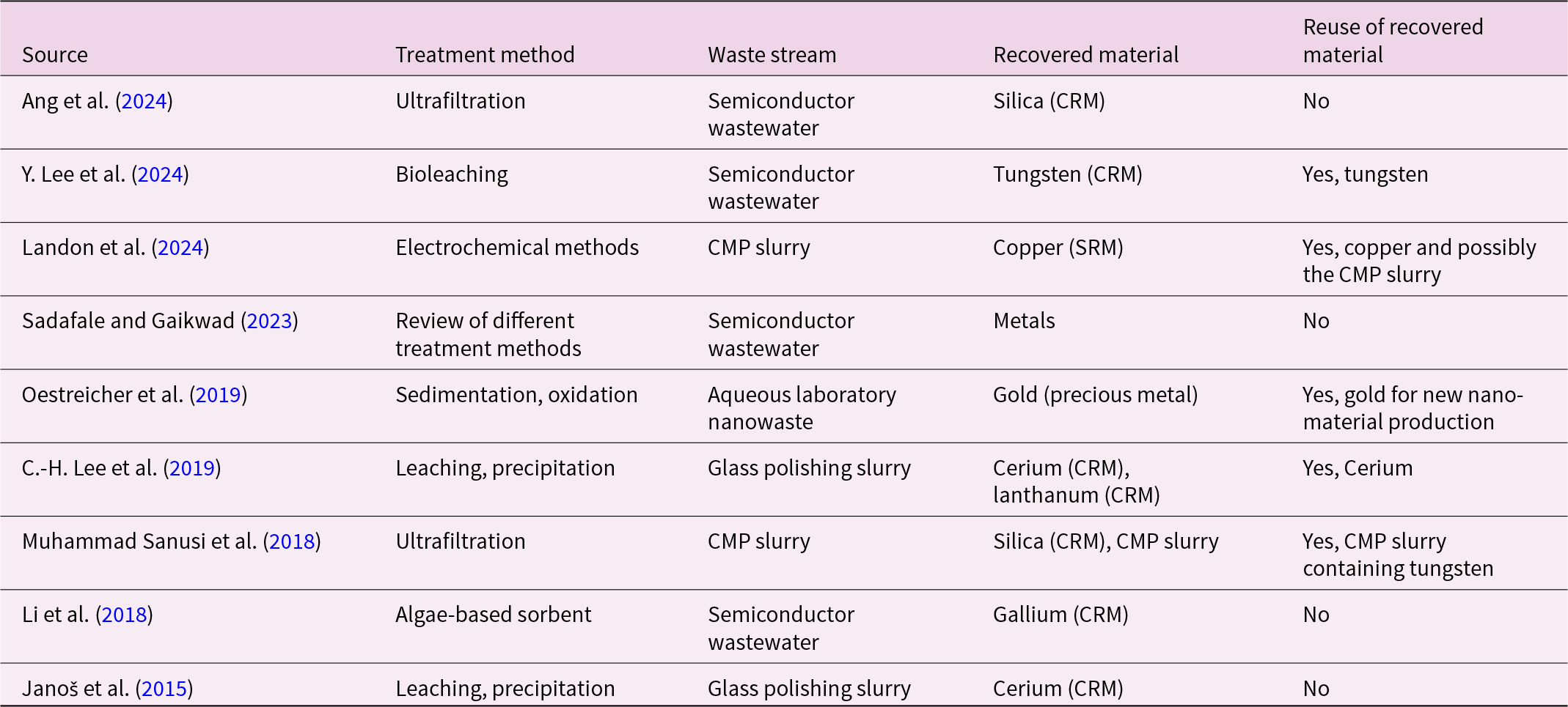
Where the previous chapter looked into activities reported by the industry, this scoping review of scientific literature examines technologies available for recovering CRMs and precious metals in the semiconductor industry (Grant & Booth, Reference Grant and Booth2009). Even though solvents are collected separately from resist removal or lift-off processes and metal-containing electroplating solutions are circulated, still many contaminants end up in wastewater streams due to the frequent cleaning, etching, and rinsing of wafers during the processing (Ni et al., Reference Ni, Zhang, Sun and Bao2023; Oh et al., Reference Oh, Lee and Lee2025). Additionally, the CMP process accounts for approximately 30–40% of the total wastewater volume in semiconductor manufacturing due to the discharge of used slurry (Venkataswamy et al., Reference Venkataswamy, Ramu and Seo2025). Besides abrasive particles (like ceria and silica) entering wastewater streams with the slurry, polished surfaces release metal particles (including tungsten and copper) into wastewater (Muhammad Sanusi et al., Reference Muhammad Sanusi, Mohd Yusoff, Seng, Marzuki and Abdullah2018). Accordingly, there is potential to recover precious metals from the semiconductor manufacturing effluents. Recovering metals is also necessary, as nanoparticles are released into wastewater from semiconductor manufacturing processes, which can accumulate in the food chain and end up in food and drinking water (Zahra et al., Reference Zahra, Habib, Hyun and Sajid2022).
Scientific literature was searched in spring 2025 using Scopus and Web of Science and a combination of keywords, such as semiconductor, wafer, nanoparticle, CMP, wastewater, deposition, thin film, glass polishing, CRM, precious metal, recycling, recovery, and circularity (e.g. semiconductor AND precious metal AND recovery). Table 3 summarizes the relevant scientific literature included in this non-exhaustive review. In addition to semiconductor industry, examples from the glass polishing industry were also reviewed, since the polishing processes applied are similar to the CMP process. Typically, the treatment of wastewaters from semiconductor manufacturing includes coagulation-flocculation, which can remove more than 90% of heavy metals from wastewater (Ang et al., Reference Ang, Teow, Chang, Mohammad and Wan2024; Sadafale & Gaikwad, Reference Sadafale and Gaikwad2023). This method is widely used for its simplicity and low cost, but the heavy use of chemicals generates large amounts of sludge, which complicates the recovery of metals for reuse (Sadafale & Gaikwad, Reference Sadafale and Gaikwad2023). Electrocoagulation has been developed as an alternative method, and though it can be effective in removing suspended solids from the wastewater, it also creates a lot of sludge, due to chemical addition (Ang et al., Reference Ang, Teow, Chang, Mohammad and Wan2024).
Summary of the reviewed scientific articles about the recovery of CRMs
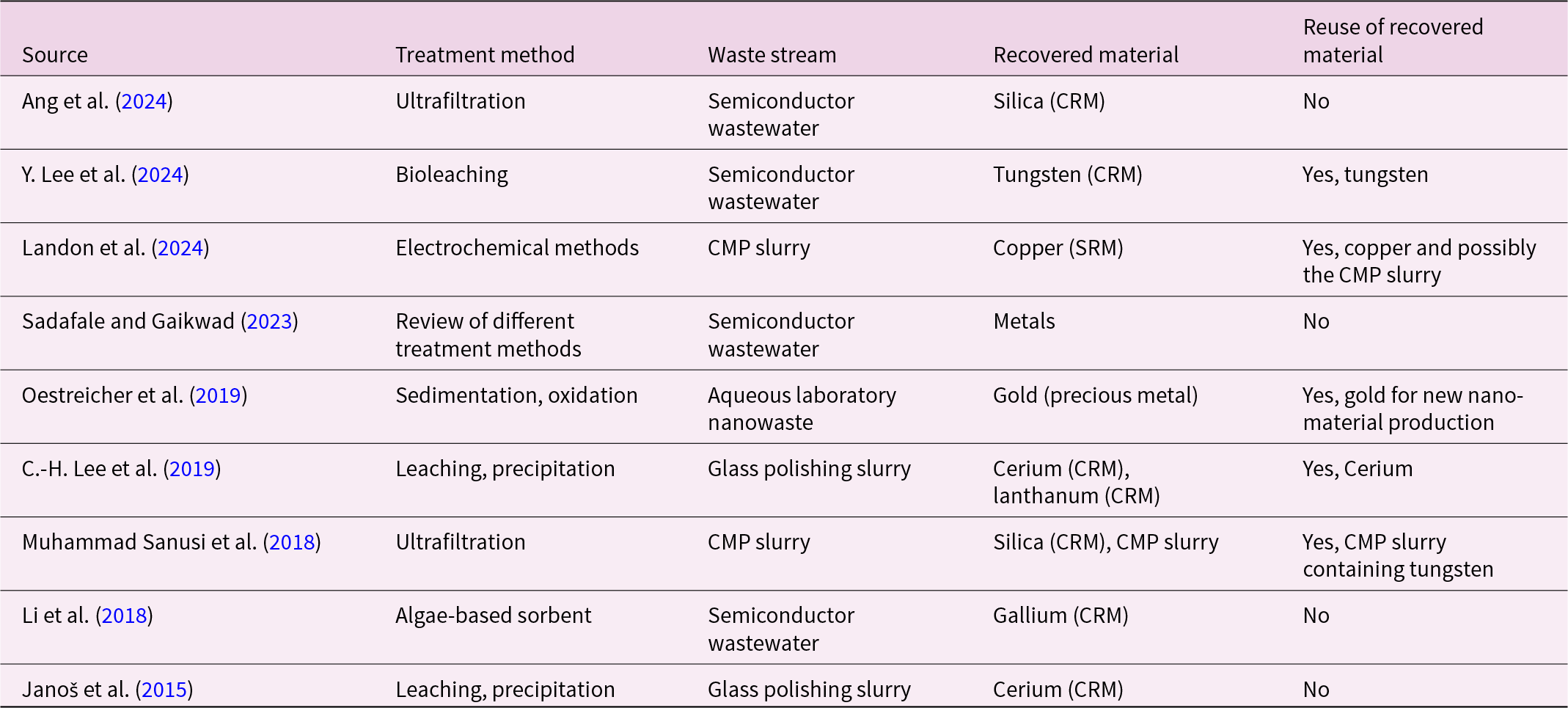
Table 3 Long description
The table summarizes nine scientific articles by treatment method, waste stream, recovered material, and whether the recovered material was reused. Waste streams are mainly semiconductor wastewater but also CMP slurry, glass polishing slurry, and aqueous laboratory nanowaste. Semiconductor wastewater studies report the recovery of silica, tungsten, gallium, and unspecified metals, using ultrafiltration, bioleaching and algae-based sorbents. One paper is a review of different treatment methods to recover metals from semiconductor wastewater. CMP slurry studies use electrochemical methods or ultrafiltration to recover copper or silica, and both report reuse, including reuse of copper and possible reuse of the slurry, and reuse of slurry containing tungsten. Glass polishing slurry studies use leaching and precipitation to recover cerium, and in one case lanthanum, with reuse reported for cerium in one study but not in another. The laboratory nanowaste study uses sedimentation and oxidation to recover gold for new nanomaterial production. Overall, reuse is more often reported for recovered metals and for slurry reuse than for silica or gallium, and one review entry lists metals without specifying which were recovered.
CRM, critical raw material; SRM, strategic raw material.
Leaching and precipitation are widely used methods in industrial waste slurry treatment to remove common heavy metals, as they are low-cost and slurry's pH can be easily adjusted in precipitation (Sadafale & Gaikwad, Reference Sadafale and Gaikwad2023). Lee et al. (Reference Lee, Lo, Sandagdorj, Gankhuyag, Popuri and Hung2019) and Janoš et al. (Reference Janoš, Kuráň, Ederer, Šťastný, Vrtoch, Pšenička, Henych, Mazanec and Skoumal2015) used leaching and precipitation with pH adjustment to extract precious metals from glass polishing slurry for reuse. Both scientific articles focused on cerium, while Lee et al. (Reference Lee, Lo, Sandagdorj, Gankhuyag, Popuri and Hung2019) additionally considered the recovery of lanthanum. Janoš et al. (Reference Janoš, Kuráň, Ederer, Šťastný, Vrtoch, Pšenička, Henych, Mazanec and Skoumal2015) achieved a cerium oxide recovery rate of about 93%, and the recovered cerium oxide was prepared to be utilized as a reactive sorbent for highly toxic organophosphate compounds. Lee et al. (Reference Lee, Lo, Sandagdorj, Gankhuyag, Popuri and Hung2019) could recover 66% of the cerium, while the recovery of lanthanum was unsuccessful. The lower recovery rate by Lee et al. (Reference Lee, Lo, Sandagdorj, Gankhuyag, Popuri and Hung2019) could be explained by the used ammonium hydroxide and sodium hydroxide for the precipitation, whereas Janoš et al. (Reference Janoš, Kuráň, Ederer, Šťastný, Vrtoch, Pšenička, Henych, Mazanec and Skoumal2015) utilized gaseous ammonia and carbon dioxide for it, since the use of hydroxides can lead to excessive precipitation, preventing metal recovery from the sludge (Sadafale & Gaikwad, Reference Sadafale and Gaikwad2023). Li et al. (Reference Li, Shadman and Ogden2018) emphasize recovering metals before the waste fractions get mixed and diluted, which requires decentralized treatment processes. They argue that methods such as precipitation, membrane filtration, and ion exchange are unsuitable for this purpose due to high reagent and energy demands and the production of contaminated sludge.
Using biosorbents for the adsorption of metals could be applicable in the semiconductor industry. For instance, Lee et al. (Reference Lee, Choi, Oh, Chung, Park and Han2024) and Li et al. (Reference Li, Shadman and Ogden2018) studied the removal of tungsten and gallium from semiconductor wastewater by using fungi and algae, respectively. According to Li et al. (Reference Li, Shadman and Ogden2018), gallium was successfully removed, even at low pH conditions. They concluded that future research should focus on finding the best way to recover gallium from algae for reuse, e.g., by desorption at different pH conditions, precipitating gallium under low-solubility pH conditions, or destroying algae in high temperatures so that gallium is left for recovery. Lee et al. (Reference Lee, Choi, Oh, Chung, Park and Han2024) investigated two alternatives for the recovery of tungsten from the leachate. The first case utilized the activated carbon-based adsorption–desorption process, where the pH of the solution determines whether the material adsorbs or desorbs on the activated carbon. The second approach for the recovery of tungsten was amine-based APT precipitation, which was modelled based on an existing study on the topic by Gao et al. (Reference Gao, Sun, Cao, Ding, Zeng, Ning, Xu and Zhang2020). Lee et al. (Reference Lee, Choi, Oh, Chung, Park and Han2024) concluded that from 10 000 litres of semiconductor wastewater, adsorption–desorption can recover 90.5 kg WO3, while amine-based APT precipitation yields up to 96.2 kg WO3.
Membrane technologies have recently gained popularity in removing impurities with removal efficiencies of 96–99% for nickel, lead, and copper (Sadafale & Gaikwad, Reference Sadafale and Gaikwad2023). In the context of semiconductors, membrane technologies have been researched, e.g., for the removal of silica. Muhammad Sanusi et al. (Reference Muhammad Sanusi, Mohd Yusoff, Seng, Marzuki and Abdullah2018) argued that about 90% of abrasive slurry goes unused in the CMP process and could be reused if metal contaminants are removed from the used slurry. They successfully demonstrated that ultrafiltration with a 50 kDa PS membrane achieved 92% retention of silica and additionally 42% retention of tungsten. According to them, the spent tungsten slurry could be reused in the CMP process after chemically adjusting it, since the slurry got diluted in the rinsing step before filtration. Reusing the CMP slurry could reduce the total amount of wastewater and lead to cost savings (Muhammad Sanusi et al., Reference Muhammad Sanusi, Mohd Yusoff, Seng, Marzuki and Abdullah2018). Ang et al. (Reference Ang, Teow, Chang, Mohammad and Wan2024) focused on ultrafiltration as well, but used a ceramic membrane plate instead of a polymeric membrane to recover silica from wastewater originating from the semiconductor industry. With this technique, they managed to recover silica with a relatively high purity of 64%, compared to the conventional method of coagulation-flocculation that obtains silica with 23% purity. Nevertheless, they did not focus on the reuse of silica but rather on removing it from wastewater to reduce the environmental burdens associated with it. Filtration can be argued to be a good, cost-efficient alternative for recovery, as chemical addition is not necessarily required (Ang et al., Reference Ang, Teow, Chang, Mohammad and Wan2024; Muhammad Sanusi et al., Reference Muhammad Sanusi, Mohd Yusoff, Seng, Marzuki and Abdullah2018).
Landon et al. (Reference Landon, Rassoolkhani, Dunn, Rentschler, Lippert, Caridi and Keleher2024) developed an electrochemical wastewater treatment method that can be used for recovering precious metals from the spent CMP slurry. Currently, their method focuses on copper removal, but according to them, other metals, such as silver, gold, or nickel, could be targeted as well. The removal of metals depends on the composition of the feed stream and the metal to be recovered, since the target metals are targeted by oxidizing or plating them in solution. Besides recycling copper, they claim that by adjusting the design and analytics of the recovery method in the future, it may be possible to recycle the slurry itself for reuse, which would reduce the overall water use of the fab. Additionally, Oestreicher et al. (Reference Oestreicher, García, Soler‐illia and Angelomé2019) studied the recovery of gold from aqueous nanowaste so that it could be reused in nanomaterial production. Their method included separating gold nanoparticles from the nanowaste by salting out and transforming it into an aqueous HAuCl4 solution. Thereafter, a reusable form of gold nanoparticles was achieved through a seeded growth approach. Furthermore, by adjusting the reduction potential of reducing agents, the method could be used to recover other noble metals as well. Although this study was conducted at laboratory scale and it was not specific to semiconductors, its simple approach could potentially be applied at industrial scale.
Overall, there are various potential methods for recovering CRMs and precious metals from the effluents of semiconductor manufacturing. The electrochemical wastewater treatment process by Landon et al. (Reference Landon, Rassoolkhani, Dunn, Rentschler, Lippert, Caridi and Keleher2024) for the recovery of copper has been commercialized by the company ElectraMet (ElectraMet, n.d.), whereas the rest of the reviewed scientific literature concentrated on small-scale experiments. The purpose of metal recovery varied among the reviewed articles, as four of the studies focused on removing pollutants from their waste streams, whereas others also considered the recyclability aspects of the recovered material (see Table 3).
3. Case study: recovering ceria from the CMP slurry using membrane technology
This case study assesses the recovery of ceria, classified as a CRM (European Commission, 2023), using membrane technology, i.e. filtration to separate ceria from the spent slurry. The industrial-scale CMP process in question is used for post-grinding damage removal of glass and surface planarization of glass-isolated Through Silicon Vias (TSV) micro electro-mechanical systems (MEMS) wafers (150 mm) after glass grinding (Kuisma, Reference Kuisma2014). The process is controlled by removal amount and the main purpose is to obtain low enough surface roughness for anodic bonding of <10 nm (Mack, Reference Mack1997). The concentration of ceria in the slurry is assumed to be 1%, which is adapted from real slurry composition.
In the baseline scenario, cerium oxide-based slurry from the CMP process ends up in wastewater and ceria is lost with it. Therefore, an alternative scenario explores a CMP process with a filtering unit for the recovery of ceria, assuming that the recovered ceria is pure enough to be reused without further treatment by mixing it with the other components of the slurry. The potential carbon footprint of both scenarios is assessed, whereas the raw materials CA is conducted for ceria together with other commonly used CRMs in the semiconductor manufacturing.
3.1. Methodology for the carbon footprint assessment
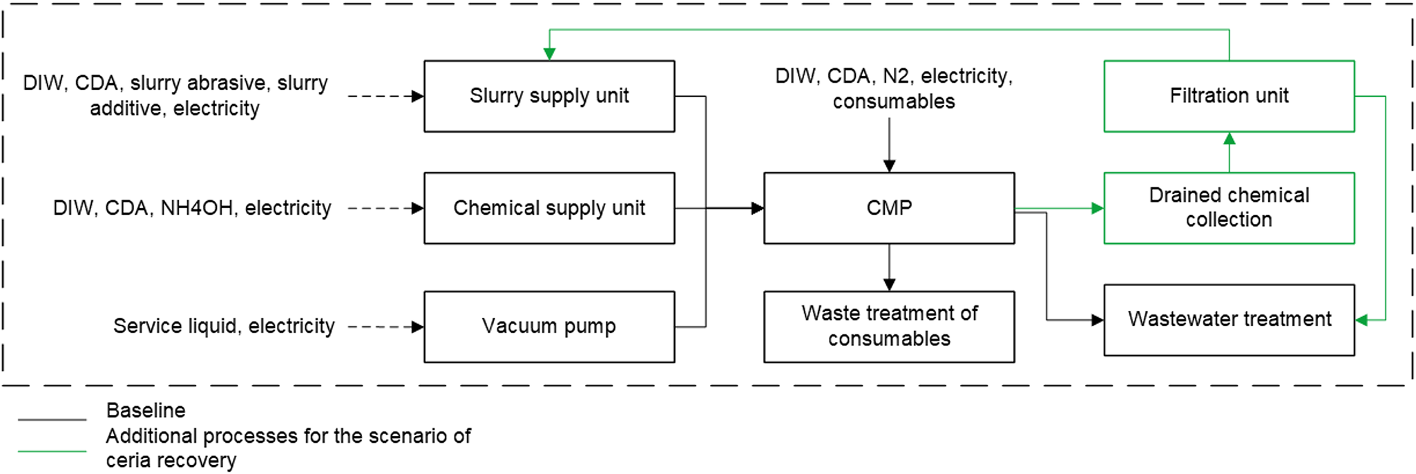
LCA approach, following ISO 14040 and 14044 standards, was used to assess the carbon footprint. Figure 1 presents the system boundary for both the baseline and the ceria recovery scenarios. The assessment focuses on the CMP process (gate-to-gate) and excludes the production of wafers. The assessment is made using SULCA software, the ecoinvent 3.10 database, and EF 3.1 impact assessment methodology. Primary data based on industrial measurements was used for the CMP process and the recovery scenario. However, the amount of ceria in the process is based on expert estimations. The carbon footprint considers only energy and materials specific to the CMP process, while cleanroom infrastructure processes, like cooling and ventilation, are excluded. The functional unit is ‘treatment of 1 cm2 of wafer with the CMP process in an industrial facility’.
System boundary of the case study for the carbon footprint. DIW, deionized water; CDA, clean dry air; NH4OH, ammonium hydroxide; N2, nitrogen.
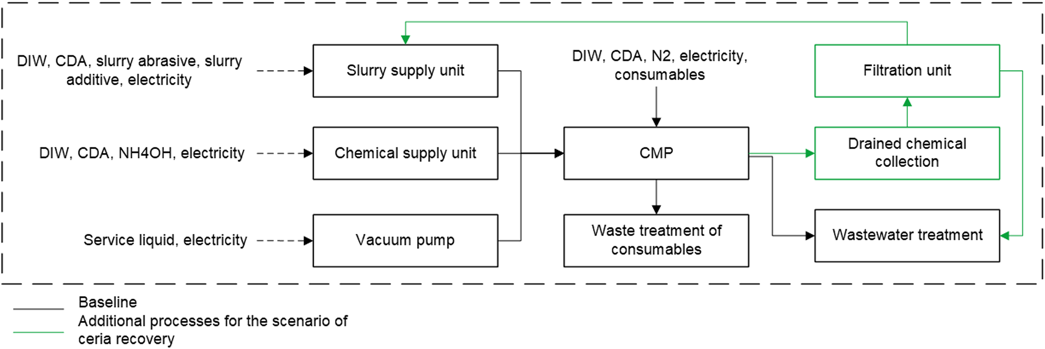
Figure 1 Long description
The flowchart illustrates the CMP process with several interconnected units. The diagram distinguishes between baseline processes and additional processes for ceria recovery scenarios. In the baseline, the process begins with inputs to the slurry supply unit, which include deionized water, clean dry air, slurry abrasive, slurry additive and electricity. The chemical supply unit receives deionized water, clean dry air, ammonium hydroxide and electricity. The vacuum pump uses service liquid and electricity. These units feed into the CMP unit, which also requires deionized water, nitrogen, electricity and consumables. The CMP unit connects to both the waste treatment of consumables and wastewater treatment. The scenario with ceria recovery includes an additional chemical collection unit which is connected to a filtration unit from where recovered ceria is fed back to the slurry supply unit.
In the baseline scenario, the CMP equipment operates at its full capacity, which is 95% of the theoretical maximum processing time, and the rest 5% is idle time. A sensitivity analysis was conducted with theoretical 80%, 50%, and 20% actual processing time for the scenario without material recovery. Table 4 categorizes energy and materials based on their use during the processing and idle time. Finnish electricity grid mix is used for the modelling. While the analysis of processing and idle times is not directly relevant to the CRM recovery scenario, variations in these factors would still influence the scenario's overall carbon footprint. For the industry, this is an important aspect since it also relates to efficiency and costs.
Division of energy and materials based on their use during the actual processing time and idle time

Table 4 Long description
The table categorizes energy and material inputs of the four processe units by whether they vary with active processing time, remain constant during both processing and idle time, or are paused during idle time. CMP is the only process with inputs adjusted to processing time, using electricity and deionized water. CMP also has inputs that stop during idle time: clean dry air, gaseous nitrogen, and CMP-related consumables. The vacuum pump has constant use during both processing and idle time, specifically electricity and service liquid, with no listed paused or processing-time-adjusted inputs. The slurry supply unit and chemical supply unit both have constant electricity use, while their material supplies pause during idle time: slurry and clean dry air for the slurry unit, and ammonia, deionized water, and clean dry air for the chemical unit. A dash indicates no items were reported for that process and usage category.
The scenario of ceria recovery is based on the baseline, for which theoretical recovery rates of 90%, 50%, and 20% are examined. The CMP process remains unchanged except for the additional steps of collecting spent slurry and filtering ceria before discharging the rest of the wastewater. Filtration unit requires additional energy in the recovery scenario. The need for ceria remains constant in both the baseline and the recovery scenario, with recovered ceria substituting for virgin ceria. It is assumed that unrecovered ceria is disposed of with wastewater, and an equivalent amount of virgin ceria is added to the system.
3.2. Methodology for the raw material CA
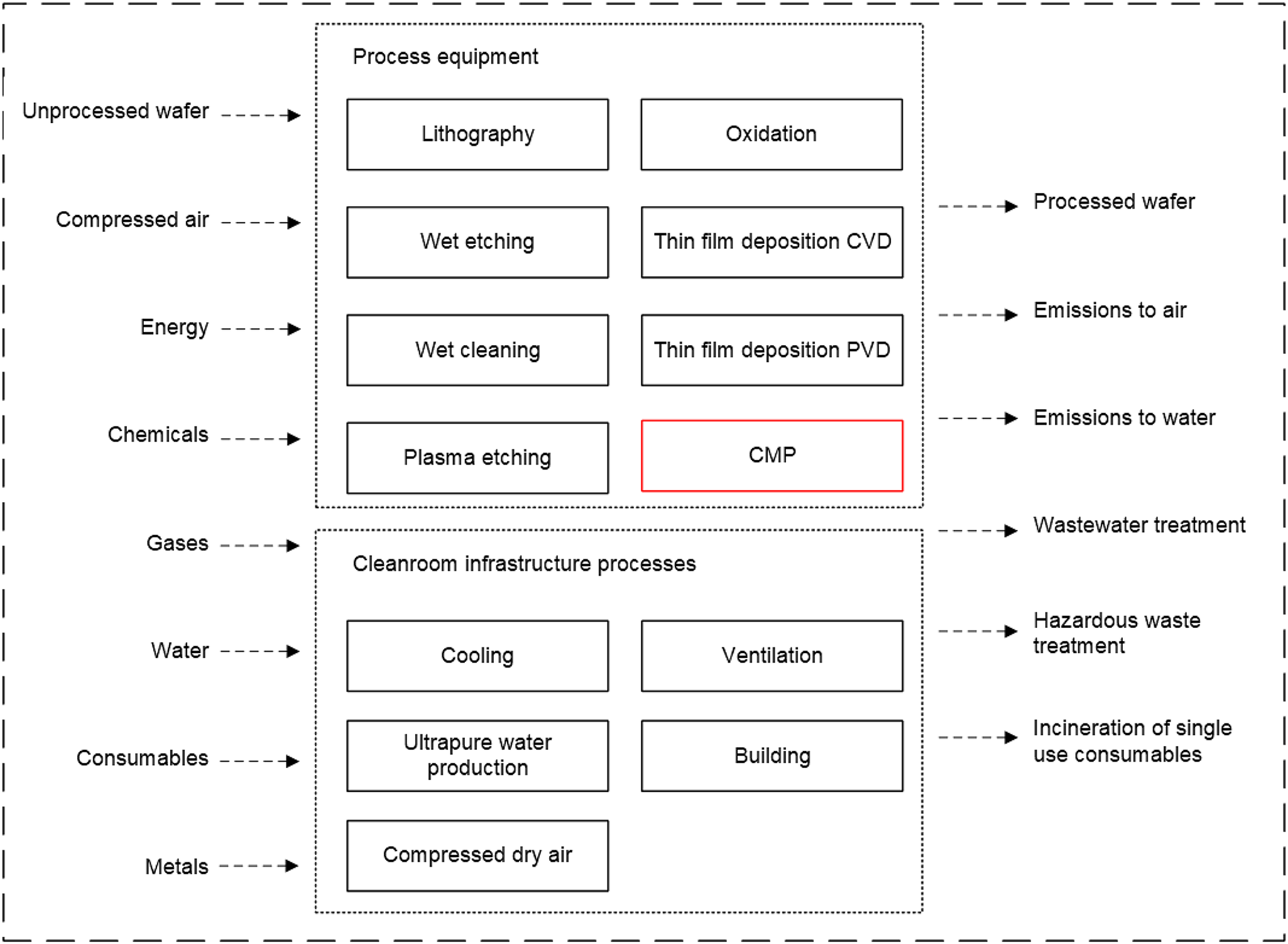
The CA considered the bill of materials (BoM) for semiconductor manufacturing, and the use of ceria was assessed in relation to other used CRMs. Figure 2 illustrates the system considered. The data on CRMs originate from a Finnish pilot cleanroom, identifying aluminium, titanium, and helium, while copper, nickel, and tungsten are added based on the LCA literature (Boyd, Reference Boyd2012; Vauche et al., Reference Vauche, Guillemaud, Lopes Barbosa and Di Cioccio2024). Copper and nickel were included as they are considered as SRMs (European Commission, 2023). The list of used CRMs is not exhaustive, and there are uncertainties related to their amounts, but assessing criticality of ceria in relation to other commonly used raw materials was important to understand the potential significance of its recovery. Silicon metal is a SRM (European Commission, 2023) and the raw material of polysilicon used in silicon wafer production. However, this CA focuses exclusively on CRMs used during wafer processing and thus excludes the silicon wafer itself, whose dominant mass share would otherwise hide the differences between the recovery scenarios.
Semiconductor manufacturing processes for which the BoM is considered in the raw material criticality assessment. CVD, chemical vapour deposition; PVD, physical vapour deposition; CMP, chemical-mechanical polishing.
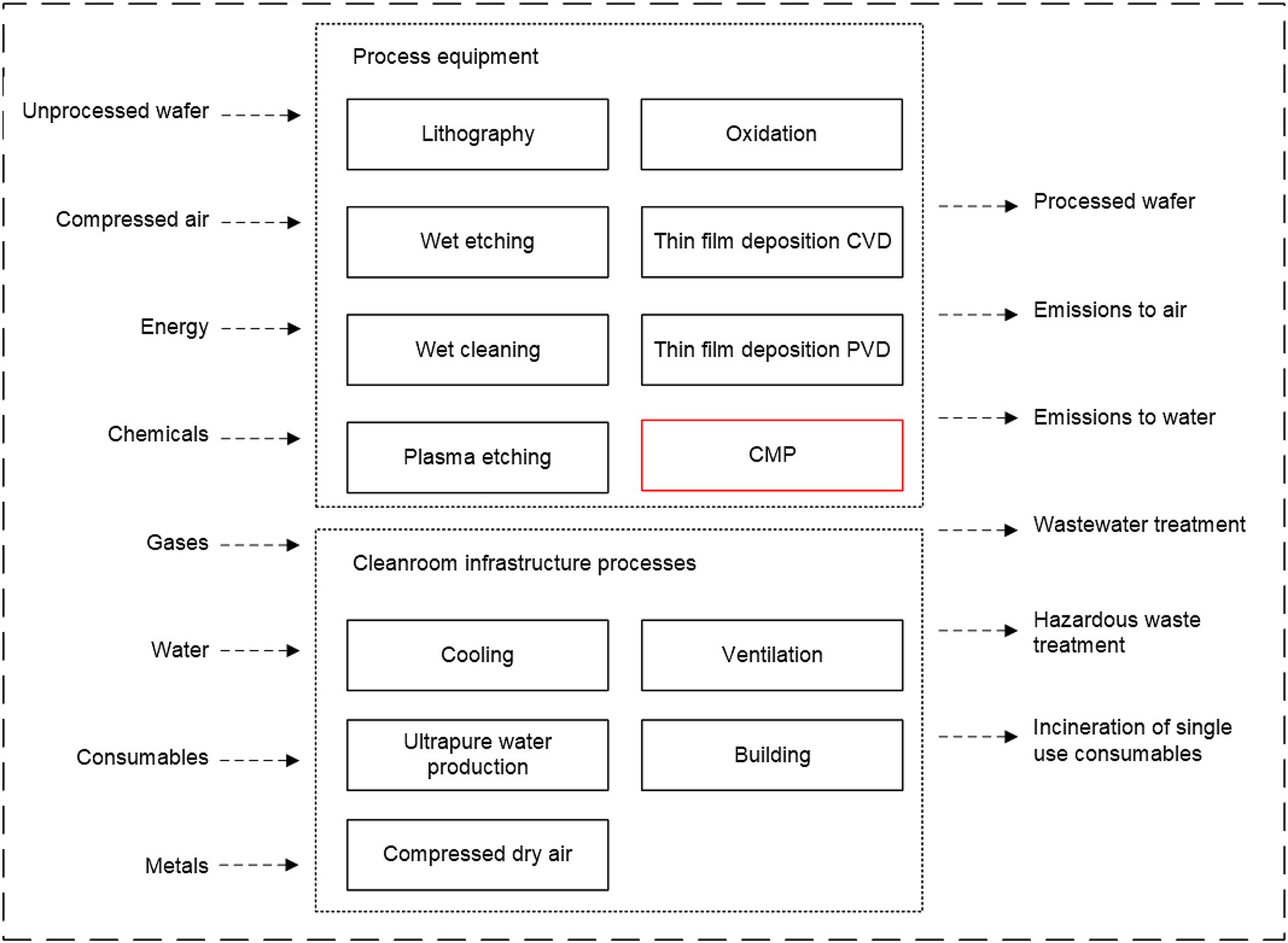
Figure 2 Long description
The flowchart illustrates semiconductor manufacturing processes and cleanroom infrastructure processes. The left side lists inputs: unprocessed wafer, compressed air, energy, chemicals, gases, water, consumables and metals. These inputs connect to two main sections. The first section, ′Process equipment,′ includes: lithography, oxidation, wet etching, thin film deposition (CVD and PVD), wet cleaning, plasma etching and CMP. The second section, ′Cleanroom infrastructure processes,′ includes: cooling, ventilation, ultrapure water production, building and compressed dry air. Outputs on the right are: processed wafer, emissions to air and water, wastewater treatment, hazardous waste treatment and incineration of single-use consumables.
Used criticality indicators were SRm, EIm, and MC, which is an integrated representation of SRm and EIm (Hackenhaar et al., Reference Hackenhaar, Moraga, Thomassen, Taelman, Bachmann and Dewulf2025). The CA follows the method used in assessing environmental impacts, where the mass of a material is multiplied by the criticality characterization factors (CFs), and total criticality is the sum of all criticality indicators of the characterized materials (Hackenhaar et al., Reference Hackenhaar, Moraga, Thomassen, Taelman, Bachmann and Dewulf2025). The calculation method for the SRm, EIm, and MC is adopted from Hackenhaar et al. (Reference Hackenhaar, Moraga, Thomassen, Taelman, Bachmann and Dewulf2025) using CF1, CF8, and CF10, respectively, and presented in Equations (1–3). The European Commission (2023) provides the used SR and EI values.
 \begin{equation}{\text{S}}{{\text{R}}_{\text{m}}}\, = \,{\sum }{\text{SR}}\,{ \times }\,{\text{mass}}\end{equation}
 \begin{equation}{\text{E}}{{\text{I}}_{\text{m}}}\, = \,{\sum}{\text{EI}}\,{ \times }\,{\text{mass}}\end{equation}
 \begin{equation}{\text{MC}} = {\sum}{\text{SR}} \times {\text{EI}}{\text{.}}\end{equation}
3.3. Results of the carbon footprint assessment
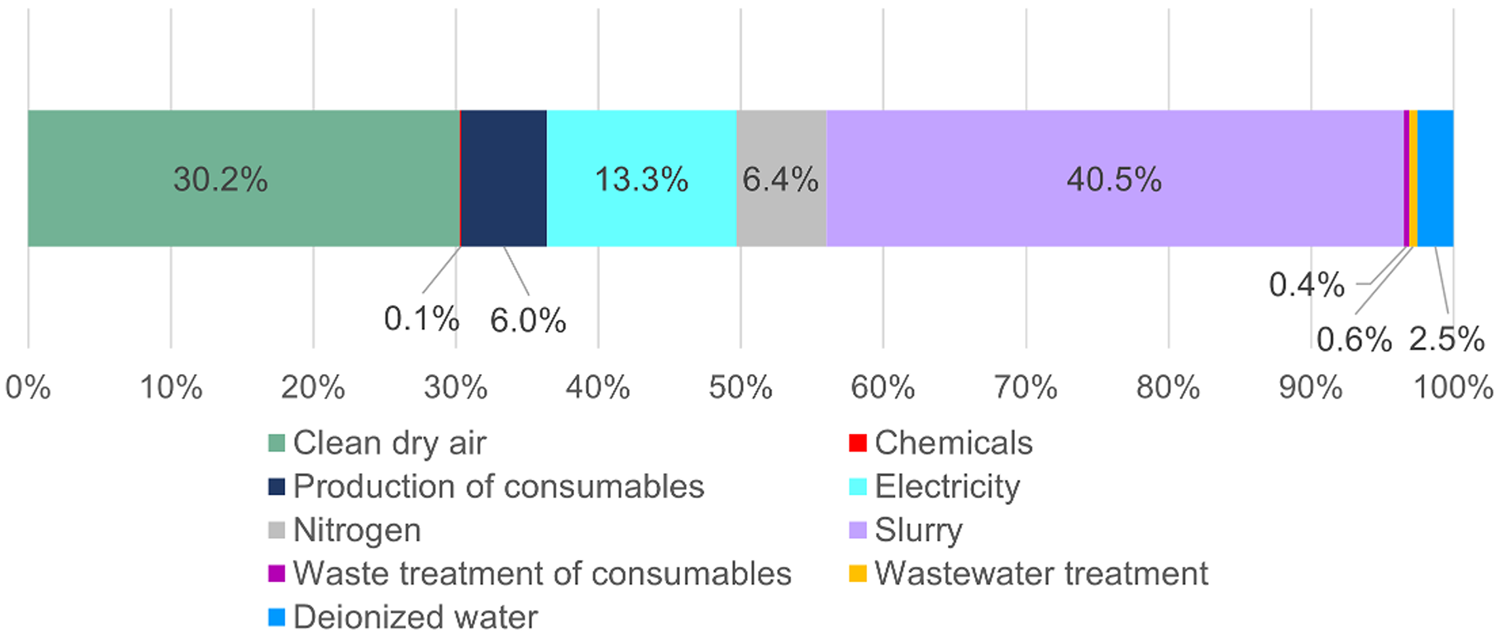
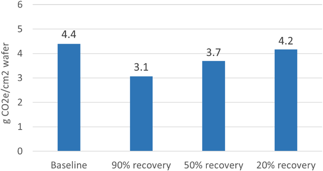
The carbon footprint results were normalized per cm2 of wafer based on assumed industrial-scale production, which builds upon measured process-level data from an industrial facility. The process-specific carbon footprint of the CMP (excl. cleanroom infrastructure) without ceria recovery (baseline) is approximately 4.4 g CO2e/cm2 wafer. Slurry (incl. ceria) and clean dry air cause most of the total GHG emissions with 40.5% and 30.2%, respectively, whilst electricity, deionized water, nitrogen gas, and production of consumables are less significant but together account for around 28% of the emissions (Figure 3). Chemicals and the treatment of waste and wastewater together contribute <1%. The sensitivity analysis shows that reducing the assumed actual processing time to 80%, 50%, and 20% increases the baseline emissions by 2.4%, 12.2%, and 48.1%, respectively, reaching 4.5, 4.9, and 6.5 g CO2e/cm2 wafer. While total annual emissions drop with lower processing time, emissions per cm2 of wafer rise due to the reduced efficiency. Moreover, including wafers in the system boundary was tested, which significantly increased the GHG emissions, with wafer-related impacts accounting for over 90%. Although wafers are central to semiconductor manufacturing, their inclusion did not serve the purpose of this study, which focused on a single process step.
Distribution of estimated GHG emissions, baseline.
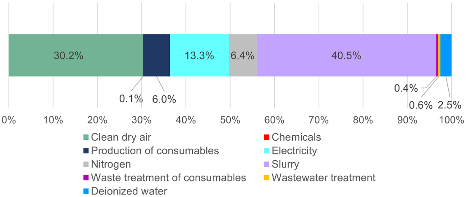
Figure 3 Long description
A stacked horizontal bar graph with one horizontal stacked bar. Horizontal axis label: percent. Horizontal axis range: 0 percent to 100 percent. The stacked bar illustrates the distribution of GHG emissions, left to right: clean dry air 30.2 percent, chemicals 0.1 percent, production of consumables 6.0 percent, electricity 13.3 percent, nitrogen 6.4 percent, slurry 40.5 percent, waste treatment of consumables 0.4 percent, wastewater treatment 0.6 percent, deionized water 2.5 percent.
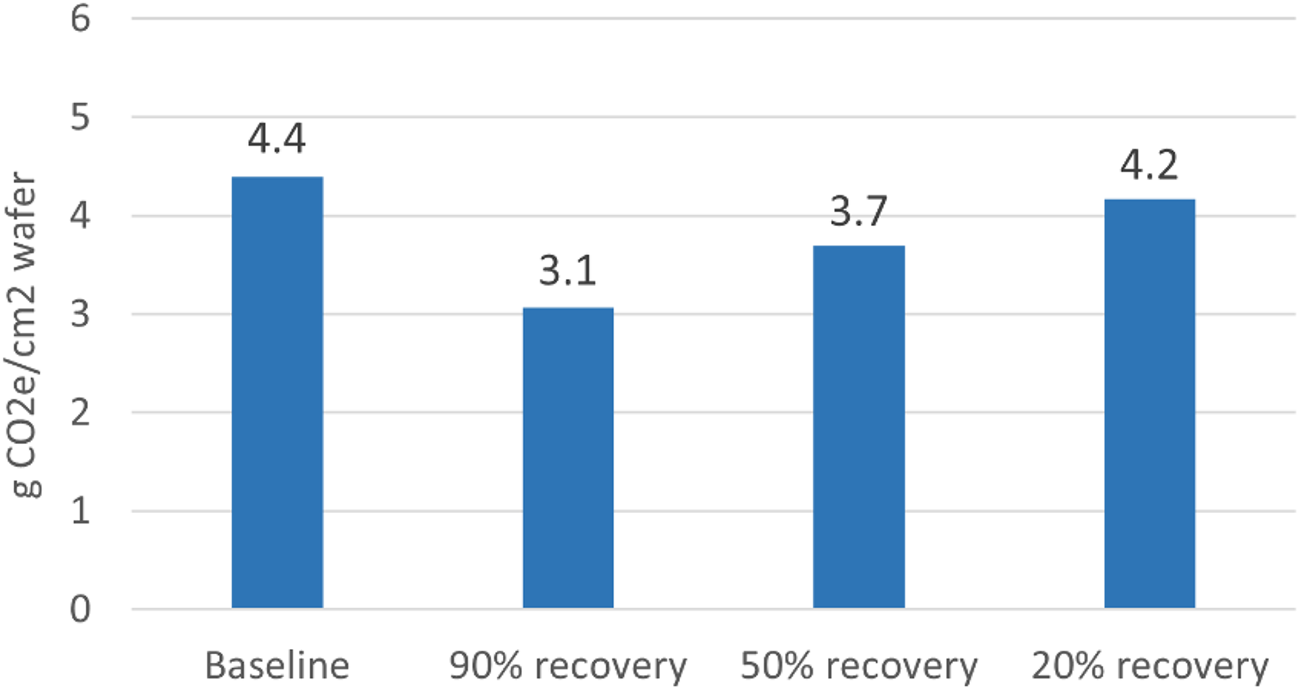
The ceria recovery scenarios show GHG emission reductions for the CMP process, although the level of reductions depends on the recovery efficiency. With 20%, 50%, and 90% recovery efficiencies, GHG emissions drop by 5.3%, 16.0%, and 30.4%, respectively, compared to the baseline (Figure 4). Higher recovery rates reduce the need for virgin ceria, lowering GHG emissions related to its production. The share of slurry-related GHG emissions of the total process-specific emissions falls from 41% in the baseline to 35%, 27%, and 12% in the scenarios of 20%, 50%, and 90% recovery efficiencies, respectively. Moreover, in the baseline, 89% of slurry-related GHG emissions are due to primary production of ceria, while in the 90% recovery scenario, it comprises only 44% of slurry's emissions. The filter unit increases the total energy use of the process by 14% compared to the baseline, contributing 2–3% of total GHG emissions in each scenario. This slightly counterbalances the emission reductions caused by the lower need for virgin ceria.
Estimated carbon footprint of the CMP for the baseline without recovery as well as for the ceria recovery scenarios (each with assumed 95% processing time).
3.4. Results of the raw material CA
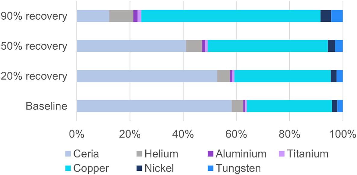
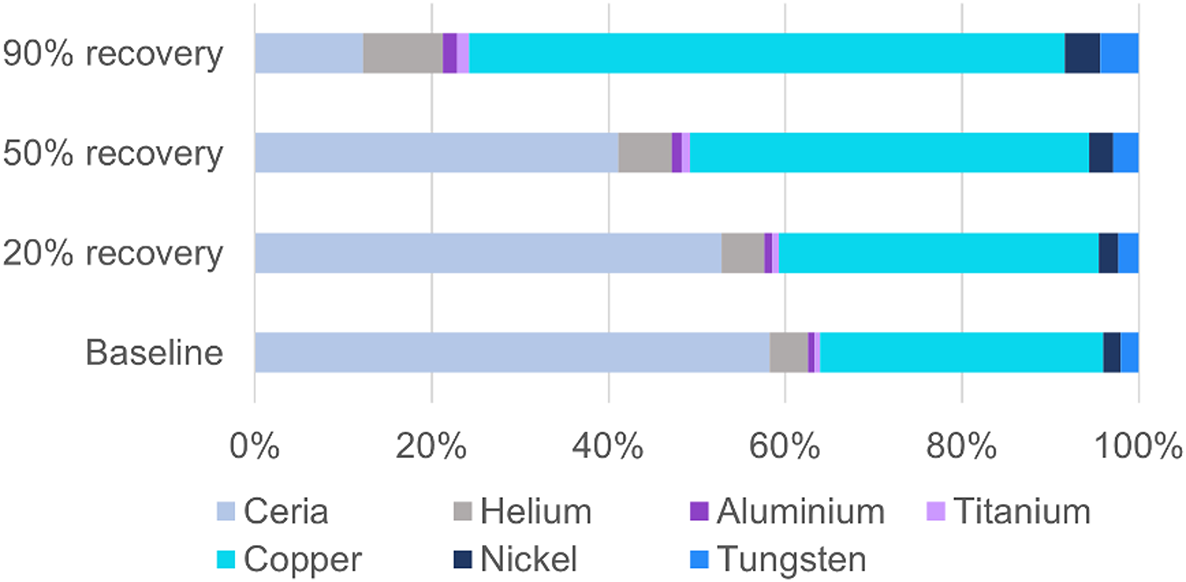
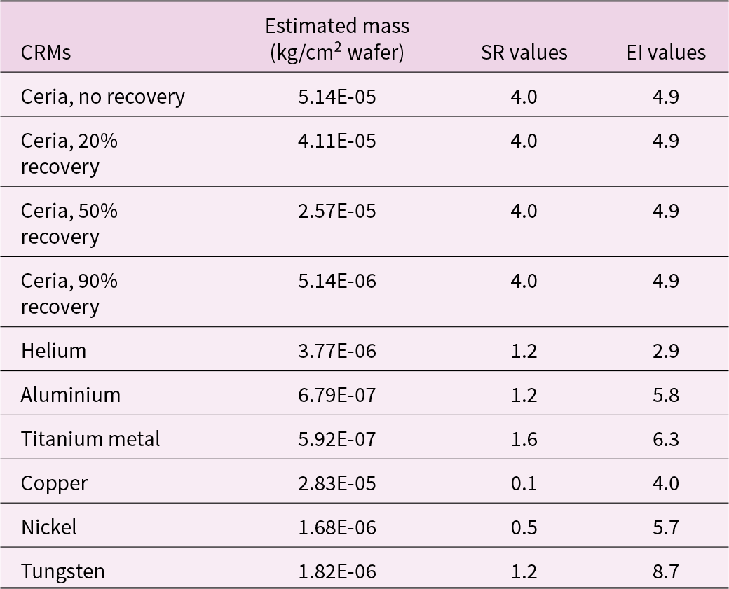
The mass of assessed CRMs is presented in Table 5 together with the SRm and EIm values (European Commission, 2023). Here, ceria refers to virgin ceria that is needed for the slurry on top of the recovered ceria. When looking solely at the mass fractions of the CRMs, the recovery of ceria reduces the mass share of virgin ceria compared to other CRMs in the manufacturing from 58% (no recovery) to 53%, 41%, and 12% with 20%, 50%, and 90% recovery rates, respectively (Figure 5). Only the amount of ceria changes in the recovery scenarios, based on how much virgin ceria is needed in the process.
Mass share of considered CRMs.
Estimated mass and SR and EI values of examined CRMs (European Commission, 2023)
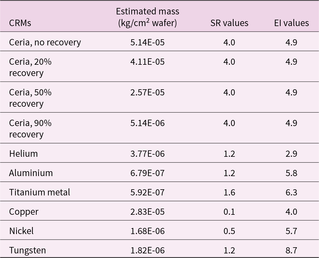
Table 5 Long description
The table lists ceria, helium, aluminium, titanium metal, copepr, nickel and tungsten with estimated mass per wafer area and two associated indicators labeled SR and EI. Ceria has the largest estimated mass, starting at 5.14E minus 05 with no recovery and decreasing stepwise to 5.14E minus 06 at 90 percent recovery, while its SR and EI stay constant at 4.0 and 4.9. Copper is the next highest mass at 2.83E minus 05 and has the lowest SR value at 0.1 with an EI of 4.0. Among the non-ceria materials, helium has the highest mass at 3.77E minus 06, while aluminium and titanium metal are the lowest masses at 6.79E minus 07 and 5.92E minus 07. EI values vary widely, with tungsten highest at 8.7, followed by titanium metal at 6.3, aluminium at 5.8, and nickel at 5.7. SR values range from 0.1 for copper up to 4.0 for all ceria scenarios, with most other materials between 0.5 and 1.6. Comparisons should note that SR and EI are presented as given indicators without definitions in the table, and only ceria includes multiple recovery scenarios.
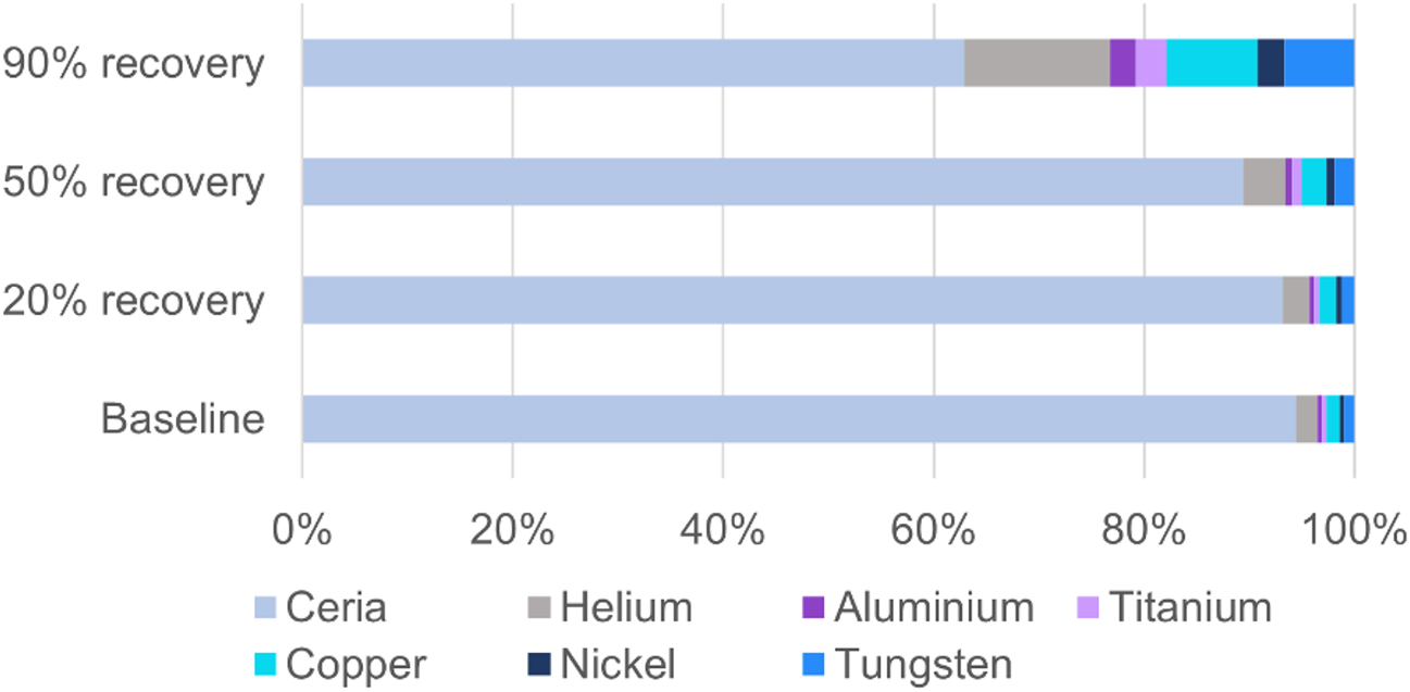
For each calculated indicator, the criticality reduces when more ceria is recovered (Table 6). With 90% ceria recovery, the SRm indicator is reduced by 85% compared to baseline, while 50% and 20% recovery result in 47% and 19% reductions. Ceria has the highest SR value and the largest mass fraction of the studied CRMs, which makes the SRm prone to high fluctuations due to ceria recovery. Without ceria recovery, ceria is, with a 94% share, the main contributor to the supply risk indicator (Figure 6). Even with 90% recovery of ceria, ceria's share of the SRm indicator remains at 63%, though the mass share of it is only around 12% of all considered CRMs.
Distribution of the supply risk (SRm) indicator results.
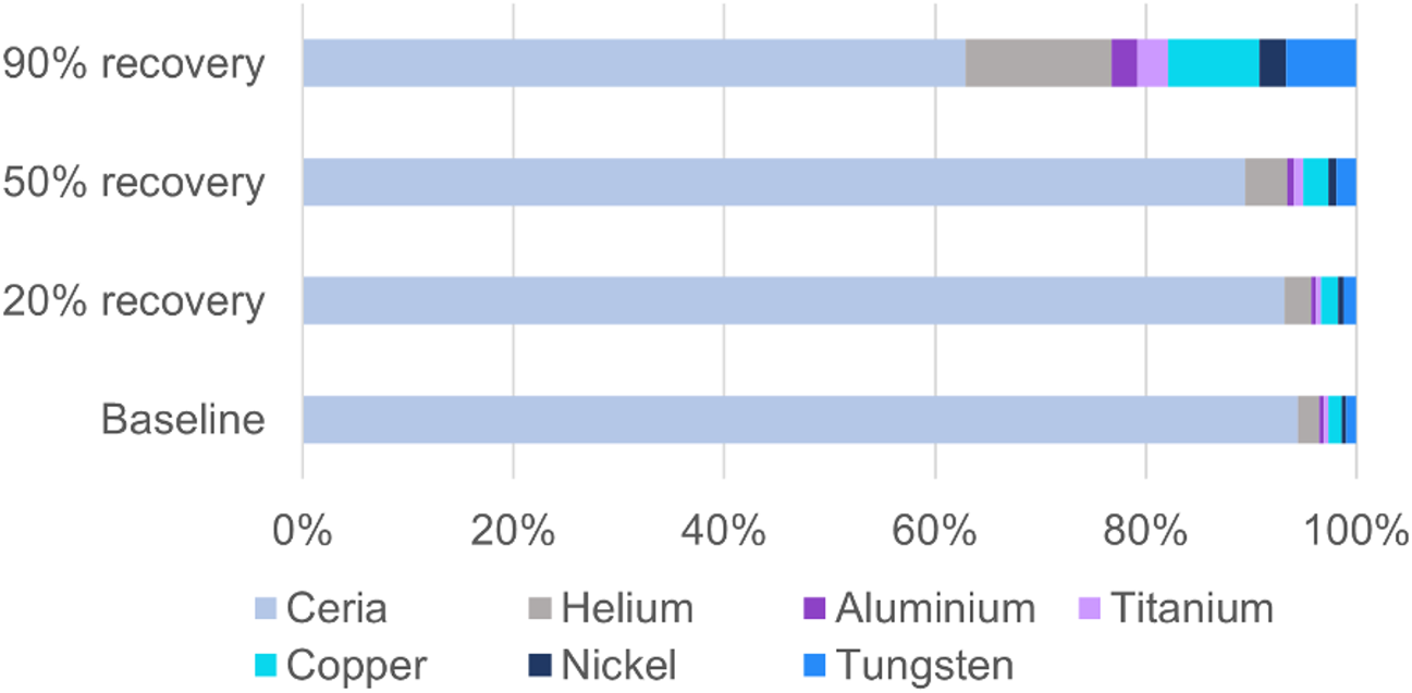
Figure 6 Long description
The stacked bar graph shows material distribution across four scenarios: baseline, 20 percent recovery, 50 percent recovery and 90 percent recovery. Each scenario is represented by a horizontal bar divided into segments for ceria, helium, aluminium, titanium, copper, nickel and tungsten. The top section highlights the dominance of Ceria, which decreases from nearly 94 percent at Baseline to about 63 percent at 90 percent recovery. Other materials like aluminium and nickel show slight increases in their shares as recovery improves. The bottom section mirrors this pattern, emphasizing the reduction in ceria′s share and the relative increase of other materials. The graph illustrates how material composition shifts with increased recovery efforts, highlighting ceria′s significant impact on supply risk.
Criticality assessment results for each indicator per functional unit (cm2 of wafer) for each scenario and the change compared to the baseline scenario

Table 6 Long description
The table reports three criticality indicators per functional unit, defined as one square centimeter of wafer, across four scenarios: baseline and 20%, 50%, and 90% recovery. Baseline values are SR 2.18E−04, EI 4.09E−04, and MC 5.22E−08. With 20% recovery, SR decreases to 1.77E−04 (down 19%), EI to 3.59E−04 (down 12%), and MC to 3.36E−08 (down 36%). With 50% recovery, SR is 1.15E−04 (down 47%), EI is 2.83E−04 (down 31%), and MC is 1.34E−08 (down 74%). With 90% recovery, SR falls to 3.27E−05 (down 85%), EI to 1.82E−04 (down 55%), and MC to 9.36E−10 (down 98%). Across scenarios, increasing recovery consistently reduces all three indicators, with MC showing the largest relative improvement. Percent changes are relative to the baseline and reflect proportional differences rather than absolute magnitude comparisons across indicators.
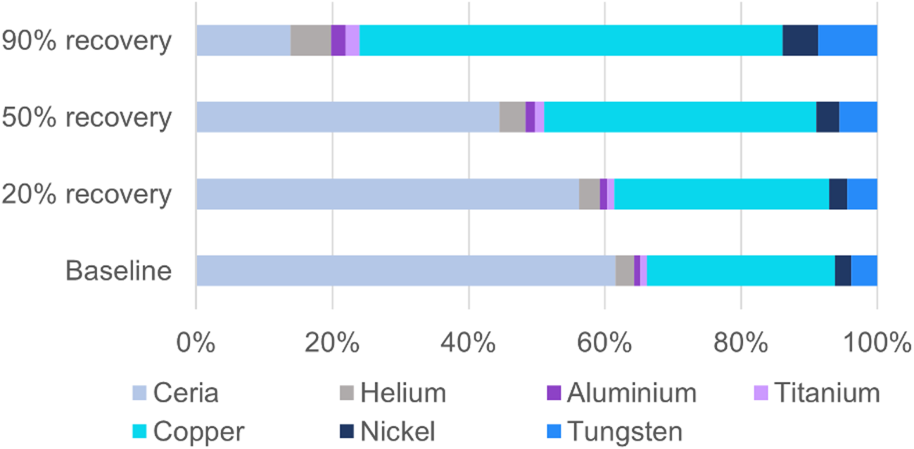
For the EIm, ceria's EI value is lower compared to most of the other assessed CRMs (Table 5). A 90% ceria recovery could only roughly halve the overall economic importance, and the lower recovery rates would decrease the EIm only by 12–31% compared to the baseline (Table 6). The distribution of CRMs for each scenario follows roughly the distribution of the mass fractions. The share of ceria of the EIm in the baseline is the highest, with 62%, compared to other CRMs, while the share of copper, as the second highest contributor, is 28% in the baseline (Figure 7). The more ceria is recovered, the less significant its role in the EIm indicator becomes (56%, 45%, and 14% for the recovery rates 20%, 50%, and 90%, respectively), leading to copper taking over with the largest share (62%) in the 90% recovery scenario.
Distribution of the economic importance (EIm) indicator.
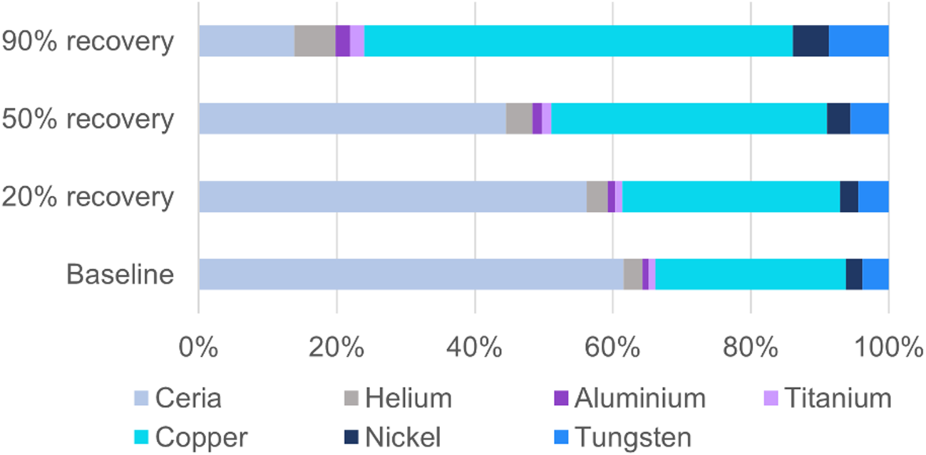
Figure 7 Long description
The stacked bar graph displays the distribution of materials in four scenarios: baseline, 20 percent recovery, 50 percent recovery and 90 percent recovery. The horizontal bars are segmented to represent different materials: ceria, copper, helium, nickel, aluminium, tungsten and titanium. The horizontal axis is labeled percent, ranging from 0 percent to 100 percent. In the baseline scenario, ceria dominates with approximately 62 percent, followed by copper at around 28 percent. As recovery increases to 20 percent, 50 percent and 90 percent, ceria′s share decreases, while copper′s share increases, becoming the largest at 90 percent recovery. The graph highlights the shift in material dominance from ceria to copper as recovery rates improve.
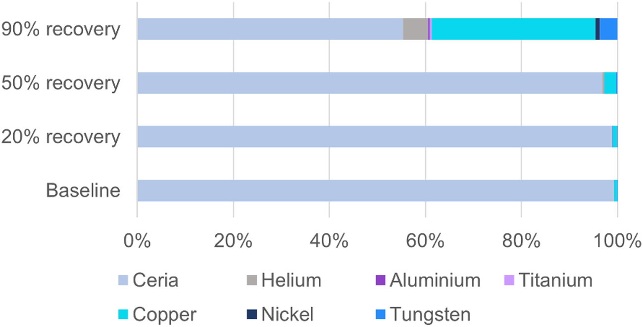
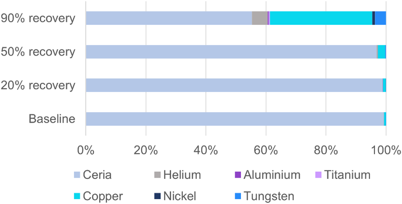
The MC indicator is sensitive to the recycling of ceria since it declines by 36%, 74%, and 98% with 20%, 50%, and 90% recovery scenarios (Table 6). Ceria covers 97–99% of the MC indicator in the baseline and the scenarios with 20% and 50% ceria recovery, while ceria's share falls to 55% in the 90% recovery scenario (Figure 8). This correlates with ceria's mass share, which ranges between 41% and 58% for the baseline and scenarios with 20% and 50% recovery, whereas it drops to 12% with 90% recovery. The sensitivity of MC to ceria can be explained by the relatively high SR and EI values for ceria and its large mass share compared to other studied CRMs. Although the SR and EI values of copper are low, its relatively high mass share is the reason it becomes apparent contributor to this indicator with 34% share of the considered CRMs.
Distribution of the material criticality (MC) indicator.
3.5. Uncertainties related to the case study
Uncertainties related to both the carbon footprint and the CA were explored qualitatively and grouped into three main categories: data, process performance, and criticality indicator-related uncertainty. This grouping distinguishes uncertainty sources by their origin, enabling more targeted interpretation of their influence on the results.
Data-related uncertainties arise mainly from the use of secondary data for studied input materials and lack of specific data sets that are important for the CMP process. These include nitrogen gas, which was modelled using data from liquid nitrogen, and polishing pads, which were modelled based on available data for polyurethane. These are assumed to lead to moderate uncertainties. Moreover, since the focus of this study was on the CMP process and related impacts, cleanroom infrastructure processes were excluded, although their inclusion could have measurable impacts on the results due to their energy-intensive nature. On the other hand, energy intensity of clean room infrastructure would be similar in both cases (with and without recovery of ceria). Moreover, the carbon footprint results were normalized per cm2 based on assumed industrial production capacity, which in reality could vary depending on the annual throughput. In practice, if the cleanroom processes were included, higher annual throughput would reduce the normalized carbon footprint, as the share of energy use from infrastructure processes and wafer processing steps, which dominate the fab's energy demand, would remain relatively constant and be distributed over more output (Guillemet et al., Reference Guillemet, Pichon and Degrenne2026).
Uncertainties specific to process performance include the assumption that filtered ceria can be directly reused in the process, but this might not be always possible without additional processing steps. Additionally, while the amount of ceria was adapted based on real slurry composition, it can differ depending on the intended use case and process, thus affecting its recovered amount and achieved GHG reductions. Furthermore, the theoretical amount of recovered ceria has high uncertainties since it depends on various process parameters, such as sludge composition and filtration velocity, thus impacting both the carbon footprint and the CA result.
Criticality indicators also come with uncertainties. The CA combined data from different sources, aiming to assess ceria's potential significance relative to other CRMs commonly used in semiconductor manufacturing. Consequently, the results are to be considered indicative. Moreover, this case study represents a single process under specific circumstances and cannot be generalized for other CMP processes. For the CA, the supply risk and economic importance indicators are very case-specific, as used CRMs in the semiconductor industry depend on the type and features of fabricated semiconductors. Also, the CA depends on the SR and EI values used, and they can become obsolete rapidly if there are substantial changes in the global situation or production quantities.
4. Discussion
The analysis of 2024 performance in the corporate sustainability reports of 11 global semiconductor manufacturers indicates that while some recovery efforts for CRMs exist from semiconductor manufacturing waste streams, they are not yet widespread. Material recovery in semiconductor manufacturing can be considered advanced practice, but it is not necessarily reflected in the reported circularity goals. The industry may not yet fully recognize the potential benefits of recovering and recycling CRMs. In the EU, its importance has been acknowledged in the Critical Raw Materials Act by the EU, which promotes the recycling of CRMs. In future, recovery rates of CRMs could be integrated into corporate-level circularity and environmental goals, supported by specific indicators and novel recovery methods. The literature review on existing recovery methods for CRMs and precious metals highlights potential methods, including membrane technologies, electrochemical treatment, and bioleaching. These methods vary in purpose, some focusing on contaminant removal while others enable the reuse of recovered materials. Although the electrochemical treatment by Landon et al. (Reference Landon, Rassoolkhani, Dunn, Rentschler, Lippert, Caridi and Keleher2024) was demonstrated at commercial scale, the other methods remain at small scale and require further development. This limited industrial applicability may partly explain the lack of CRM recycling perspective in the studied corporate sustainability reports. Increasing geopolitical pressures might raise interest in such methods in future.
The LCA case study explored potential GHG emission reductions from applying membrane technology to recover ceria from the CMP slurry for closed-loop recycling. The CMP slurry was the largest single contributor (38%) to the carbon footprint specific to CMP process, excluding cleanroom infrastructure. The sensitivity analysis implies that the carbon footprint per wafer area increases significantly as processing disruptions keep equipment running with reduced output. The recovery of ceria from the slurry has the potential to reduce the estimated GHG emissions of the CMP process by 27% in the scenario with 90% recovery.
The CA for ceria suggests that supply risk is more critical indicator than economic importance since the overall criticality decreases by 85% for the former and only 55% for the latter in the scenario with 90% recovery. For the economic importance, with 90% ceria recovery, copper surpasses ceria as the most significant CRM. The MC indicator achieves even higher reduction in the overall criticality (98% for 90% recovery scenario), since it is a combination of supply risk and economic importance. Among the assessed CRMs, ceria faces the highest supply disruption risks due to reliance on few countries for mining and refining.
According to the author's knowledge, this study is one of the first screening studies focusing on CRM recovery in the semiconductor industry, combining different methods, and addressing technological aspects together with potential climate impacts and criticality of raw materials. Hopefully, it provides a starting point for more comprehensive examinations of this topic. The reviews on sustainability reports and literature are limited by their non-exhaustive nature, so there might be variability in the recovery practices and technologies beyond the ones discussed in this study. Moreover, the case study represents a single CMP process, from which the data and results cannot be generalized. As CA is always highly case-specific, generated results need to be analysed in a case-specific context. Future CAs could benefit from testing different methods (e.g. GeoPolRisk) and varying quantities of CRMs to assess the sensitivity of CRMs and the used criticality indicators.
5. Conclusion
This study focused on the recovery of CRMs in the semiconductor industry, with a particular focus on the CMP process. Although the recycling of CRMs is not yet well-established across the industry, our case study indicates that ceria recovery has the potential to reduce CMP-related GHG emissions and increase the resilience of the semiconductor industry by mitigating the risks associated with CRMs. Issues related to criticality can impact the semiconductor industry globally when the supply of CRMs is concentrated in a few countries, since possible disruptions in supply chains can lead to increased costs, delays in production, and revenue losses. Thus, more effort and technological development are needed to support CRM recovery, thereby making the industry less dependent on vulnerable supply chains and virgin raw materials. This study focused on one specific CRM and processing step, excluding the cleanroom infrastructure. The results show that the recovery of ceria from the slurry has the potential to reduce the estimated GHG emissions of the CMP process. Future research should take a more comprehensive look at the environmental impacts of semiconductor manufacturing and consider what kind of impacts and benefits could be gained by implementing different circularity strategies. Also, the impacts of recycling CRMs could be assessed for other semiconductor fabrication processes and for various types of semiconductors to strengthen the knowledge base. Lastly, the applicability of circularity indicators in the semiconductor industry should be assessed in more detail.
Acknowledgements
The authors would like to thank Murata Electronics Oy for providing measured data of the chemical-mechanical polishing process and Sofi Filtration Oy for providing measured data of the electricity consumption of the filter unit for the ceria recovery scenarios.
Author contributions
N. H. was the primary researcher for this paper, including research design, data collection, modelling, and analysis. N. H. wrote the article and created the figures and tables. M. A. and H. P. contributed to the research design with methodological insights and clarifications, edited the paper, and supervised the work.
Funding statement
This research was conducted as part of a Business Finland-funded project ‘ZeroChip’ (2024–2026).
Competing interests
The authors declare no conflict of interest.



 Open access

