

1. Introduction
The polarity of III-V nitride semiconductors is a critical issue that has hindered improvements in nitride materials and the performance of devices. The quality of the wurtzite GaN films shown in Figure 1 can be varied by the polarity, because both the incorporation of impurities and the formation of defects are related to the growth mechanism, which in turn depends on the polarity of the surface. The occurrence of a two dimensional electron gas (2DEG) and the optical properties of hetero-structures of nitride-based materials are influenced by the internal field effects caused by spontaneous and piezo-electric polarizations. Devices in all of the III-V nitrides are fabricated on polar {0001} surfaces. Consequently, their characteristics depend on whether the GaN films exhibit Ga- (+c) or N - (−c) face polarity. Therefore, it is very important to be able to determine and control the polarity of GaN.
Schematic illustration of GaN wurtzite crystal structure exhibiting the polarity along the c-axis. The small and large spheres indicate Ga and N, respectively. GaN with Ga-face (+c) polarity on left side and GaN with N-face (−c) polarity on right side. When the direction of the three bonds of the III-element is towards the substrate, the polar structure is defended as +c polarity. On the other hand, when that of the bonds is upward against substrate, it is defined as having −c polarity. The termination element on the surface is not specified unless it is explicitly mentioned in this article.

Nitride films have conventionally been grown on sapphire substrates by using a number of growth techniques, such as two-step metallorganic chemical vapor deposition (MOCVD) Reference Amano, Sawaki, Akasaki and Toyoda[1], molecular beam epitaxy (MBE), pulsed laser deposition (PLD) and hydride vapor phase epitaxy (HVPE). Figure 2 shows optical microscope images for our MOCVD-GaN films with both smooth and hexagonal-facetted surfaces, which are due to +c and −c polarity, respectively. The results of our study compare well with the standard frameworks for the polarity provided by Hellman Reference Hellman[2] and the resulting GaN samples are acceptable within this context.
Optical microscope images of (a) +c GaN and (b) −c GaN films on sapphire substrates. The surface morphology of typical +c and −c GaN films are smooth and hexagonal facetted, respectively. The polarity was determined by the CAICISS method described in Sec. 2.4.

Some researchers have classified the polarity of GaN films by the growth method used to obtain them, in that films grown by MOCVD and MBE have +c and −c polarity, respectively. In addition, nitridation of sapphire substrate has often been regarded as a way to obtain −c GaN films. However, different groups using the same growth technique have sometimes found that there are conflicts between the polarities that result from their experiments. When GaN films are grown by MBE (in which the nitridation process is commonly used) +c GaN films are the likely outcome under III-rich conditions. On the other hand, although the sapphire substrate was not intentionally nitrided, a hexagonal-facetted surface (indicating −c polarity) was observed for a GaN film on a thin GaN buffer layer grown by MOCVD and reported by Nakamura Reference Nakamura[3]. In another report by Uchida et al., a smooth surface (indicating +c polarity) was obtained for a GaN film grown on a thicker buffer layer by MOCVD, even though the substrate was intentionally nitrided Reference Uchida, Watanabe, Yano, Kouguchi, Tanaka and Minagawa[4]. These confusions in controlling the polarity are a feature of the growth experience of many research groups.
We have studied the role of the LT-buffer layer and the implications of each part of the process for the growth of GaN films by two-step MOCVD. The conditions used to treat the substrate and the deposition and annealing of the LT-buffer layer have been found to correlate with the polarity of the grown layers. Through these studies, ‘recipes’ to control the polarity of the layers have been suggested. Indeed, the polarity can be managed from +c through to −c, including mixed polarity layers, by systematically varying the conditions used in the MOCVD process (Sec. 4). This paper will critically review the status of polarity control for the MBE, PLD and HVPE growth methods, as published in the literature. General conditions that are decisive for the determination of polarity are itemized for each growth method. Comparing the recipes used in MOCVD growth with the features identified for the other methods, we will examine whether or not the implications derived from our evaluation of the MOCVD process are equivalent to those noted for the other methods. The correlation between polarity and the growth conditions will be discussed in order to clarify the various confusions experienced in the determination of polarity during GaN growth.
In Sec. 2, techniques for evaluating the polarity are summarized in chronological order, and their specific features are identified. We used coaxial impact collision ion scattering spectroscopy Reference Katayama, Nomura, Kanekawa, Soejima and Aono[5] (CAICISS) to characterize the polarity. The important features and the advantages of CAICISS are mentioned. The case of InGaN multi-quantum wells is examined to demonstrate the potential of CAICISS analysis. In Sec. 3, the correlation between the polarity and the growth conditions in terms of substrate treatment and buffer layer preparation is summarized for GaN films deposited by MBE, PLD, and HVPE. In Sec. 4, variations in the LT-buffer layer depending on the growth conditions in MOCVD are examined with respect to controlling the polarity. While discussing the implications of each growth process in MOCVD, ‘recipes’ to manage the polarity of the GaN films are proposed. By comparing these recipes with the relevant details of other techniques, it will be concluded that the polar structures at the interfaces of both the sapphire substrate and the annealed LT-buffer layer are the most important aspects of polarity management. Our focus moves on in Sec. 5 to a study of the polarity-dependence of the properties of GaN films and of device performance. The dependence of the properties of GaN on the polarity properties is elucidated with respect to both impurity incorporation and defect formation. The effect on device performance of the internal electrical field due to the polarity in the material is reviewed, focusing on the interface between the metal and the III-V nitride semiconductors. Our work is finally summarized in Sec. 6.
2. Characterization of GaN polarity
We selected CAICISS analysis to determine the polarity of GaN out of the many techniques that are available. After summarizing the various techniques and their features, the advantages of CAICISS are introduced by presenting a study of InGaN single quantum well (SQW) using CAICISS in this section.
2.1 Notation of GaN polarity
When three of the bonds on a Ga atom with tetrahedral coordination face towards the substrate, the polarity is typically called Ga-face. In contrast, when three bonds face in the growth direction, the material is termed N-face, as shown in Figure 1. There are four possible surface structures in wurtzite III-V nitrides, considering both the termination atom and the crystallographic polarity, e.g., Ga-terminated N-face polarity. Although the terms Ga- and N-face, Ga- and N-termination or A- and B-face have been used as a sign of polarity, it is very complicated to distinguish the polarity from the termination atoms, though Seelmann-Eggebert et al. do use ‘termination’ to represent the polarity Reference Seelmann-Eggebert, Weyher, Obloh, Zimmermann, Rar and Porowski[6]. Furthermore, since AlN, InN and their alloys also need to be considered, the polar structure with the three bonds of III-atom facing toward the substrate is defined as +c polarity and the opposite as −c polarity in this paper. The termination atoms are not specified unless they are mentioned explicitly.
2.2 Spontaneous polarization of nitride semiconductor material
The wurtzite symmetry is too low to cause an equivalent electronic structure of charge density for all 4 bonds. Even for a wurtzite material with ideal lattice constant ratio of ‘c/a’, spontaneous polarization may still occur. In hexagonal GaN, the strong ionicity between Ga-N bonds results in larger spontaneous polarization along the c-axis and slightly shorter value of c/a ratio (The lattice constants of strain-free hexagonal GaN are a = 3.189 and c = 5.185 Å.). The amount of sheet charge density induced by the spontaneous polarization is considered to be −0.029 C/m2 Reference Bernardini, Fiorentini and Vanderbilt[7] corresponding to ~3 MV/cm of internal electric field (conversion using the dielectric constant of GaN). Actually, the band profile of the GaN must be flat due to the influence of both the surface states and the carriers, except in the surface region Reference Karrer, Ambacher and Stutzmann[8]. The surface charge density caused by the spontaneous polarization is estimated to be in the order of 1013 cm−2. Hence, if a surface state density of approximately 1014−1015 cm−2 is reduced down to 1013 cm−2 by a certain surface treatment for GaN thin films (~100nm) with a carrier density of less than 1017 cm−3, it is expected that the depth of the depletion layer from the surface should extend to approximately 100nm, which is comparable to the film thickness.
There is a positive or a negative polarization charge at each interface of the multi-quantum-wells (MQWs) that are used as the active layer of LEDs and LDs. The band decline of a very thin well and barrier layer should become mutually opposite, taking into account the flatness of the Fermi level and the depth of the depletion layer. The strength of the electric field within the InGaN active layer has been estimated experimentally to be 0.35 MV/cm from the peak shift of the PL spectra of MQWs with various thickness of wells Reference Chichibu, Abare, Minsky, Keller, Fleischer, Bowers, Hu, Mishra, Coldren, DenBaars and Sota[9]. Since the spontaneous polarizations of InN and GaN are very close, the internal electric field in the InGaN/GaN system is mainly caused by the difference in their piezoelectric polarizations; e33 (GaN: ~0.4C/m2, InN: ~1C/m2 Reference Bernardini and Fiorentini[10]). In contrast, the formation of a 2DEG of up to 1013 cm−2 at the interface of the AlGaN/GaN system cannot be explained by piezoelectric polarization alone. The effects of spontaneous polarization must be taken into consideration, owing to the large difference in the spontaneous polarizations between AlN (−0.081C/m2) and GaN Reference Maeda, Nishida, Kobayashi and Tomizawa[11].
Thus, a band profile of a hetero-structure of III-V nitrides can be modified by a combination of both the piezoelectric and spontaneous polarizations of the materials (discussed in Sec. 5). Since the influence of spontaneous polarization is sufficiently large in III-nitride system, the evaluation of the polarity is also important when designing for optimum device performance.
2.3 History of polarity evaluation
2.3.1. 1984-1994: XPS and thermal stability
Techniques that have been used for the evaluation of GaN polarity are listed in chronological order in Table I (a). The relationship between the growth conditions (and also the growth method) and the resulting polarity is presented. The first characterization results came out in 1988, two years after better quality GaN films were deposited by the development of the LT-buffer layer. Sasaki et al. deposited GaN films on both the Si and C faces of 6H-SiC substrates by MOCVD, and their polarities were determined by the dependence of the Ga signal intensity detected with angle-resolved x-ray photoelectron spectroscopy (XPS) Reference Sasaki and Matsuoka[12]. The surface morphologies of the samples on Si- and C-face SiC substrates were either featureless or hexagonal facetted. GaN films deposited on Si- and C-face 6H-SiC substrates were expected to show +c and −c polarity, respectively, according to the relationship of the electron negativity of Si and C Reference Ren and Dow[13] Reference Ren and Dow[14]. However, they determined the polarity of the former and the latter as −c and +c polarity, respectively. This misjudgment might possibly have been caused by an immature understanding of oxygen adsorption on the polar surface of GaN (refer to Sec. 5.1).
List of techniques for evaluating GaN polarity in chronological order. The relationship between growth conditions and the resulting polarity is also represented.

7 years later, Sun et al. found that a GaN film deposited on the Si-face of a 6H-SiC substrate was unstable in an H2 ambient at 600°C Reference Sun, Kung, Saxler, Ohsato, Bigan, Razeghi and Gaskill[15]. This GaN sample was determined to have +c polarity due to the electron negativity of Si and C, in contrast with Sasaki's conclusion. We also confirmed the instability of +c GaN under these conditions Reference Fuke, Teshigawara, Kuwahara, Takano, Ito, Yanagihara and Ohtsuka[16]. However, we felt that the window of the conditions used for annealing temperature, time and gas ambient seemed to be very narrow. Therefore, this technique was difficult to use generally for determining the polarity. In 2001, Koukitsu et al. measured the decomposition rate of +c and −c GaN samples in N2 or H2 gas ambients using the microgravity method Reference Koukitu, Mayumi and Kumagai[17]. GaN with +c polarity decomposed faster at lower temperatures (800-850°C) than GaN with −c polarity (900-950°C), which was consistent with Sun's report and Hellman's standard framework.
2.3.2. 1996: CBED
The investigation of polarity began intensively in '96, when the first GaN blue laser diode was developed using MOCVD and when better quality GaN was also being attempted to be grown by MBE. A convergence beam of electron diffraction (CBED) technique based on TEM Reference Ponce, Bour, Young, Saunders and Steeds[18] Reference Liliental-Weber, Kisielowski, Ruvimov, Chen, Washburn, Grzegory, Bockowski, Jun and Porowski[19] was mainly used to determine the polarity by studying asymmetric diffraction spots of (0002) and (000
-
1. MOCVD- and MBE-GaN films were likely to have +c and mixed polarity-containing inversion domains (IDs), respectively Reference Romano, Northrup and O’Keefe[20].
-
2. Nitridation of the sapphire substrate in MOCVD might result in a −c GaN film with a rough surface Reference Rouviere, Arlery, Niebuhr, Bachem and Briot[21]
-
3. The dependence of various properties on the polarity was revealed Reference Keller, Keller, Wu, Heying, Kapolnek, Speck, Mishra and DenBaars[22] Reference Ponce, Bour, Gotz and Wright[23].
Claims 1 and 2 indicate the importance of the growth process, as discussed in Sec. 4, and claim 3 is related to the dependence of impurity adsorption on the polar surface, as discussed in Sec. 5
In order to extend the possibilities of techniques based on the TEM, efforts have been made continuously to observe atomic alignment with high-resolution image matching Reference Stirman, Ponce, Pavloska, Tsong and Smith[24], to introduce micro-channeling effects during EDS analysis Reference Jiang, Eustis, Cai, Ponce, Spence and Silox[25], to detect the N K-edge and Ga L-edge during EELS analysis Reference Kong, Hu, Duan, Lu and Liu[26], or to count diffracted electrons quantitatively Reference Zandbergen, Janzen, Zauner and Weyher[27]. The polarity can also be evaluated by these new approaches.
2.3.3. 1997-1998: Surface reconstruction, chemical stability and CAICISS
There were two interesting reports in '97. One of these, which highlighted the temperature dependence of the surface reconstruction on the polarity, was carried out by Smith et al. Reference Smith, Feenstra, Greve, Neugebauer and Northrup[28]. Held et al. confirmed this surface reconstruction by RHEED observations of bulk GaN samples for which the polarity had been rigorously identified Reference Held, Nowak, Ishaug, Seutter, Parkhomovsky, Dabiran, Cohen, Grzegory and Porowski[29]. RHEED patterns that were characteristic of (1×1) and (2×2) reconstructions for −c and +c polar surfaces respectively were observed against the [11
Another technique involves the chemical stability of the −c GaN surface in alkali solution Reference Weyher, Müller, Grzegory and Porowski[32]. Apparently, −c GaN films are etched in KOH or NaOH, while +c GaN is inert to these solutions. The polarity that was determined by investigating the chemical stability was consistent with that determined by using hemispherically-scanned x-ray photoelectron diffraction (HSXPD) Reference Seelmann-Eggebert, Weyher, Obloh, Zimmermann, Rar and Porowski[6]. We reported the mechanism for the selective etching, in that OH- in solution would promote etching, attacking one back-bond of the Ga that was bonded to the nitrogen on the −c polar surface Reference Li, Sumiya, Fuke, Yang, Que, Suzuki and Fukuda[33]. The etching effects that originate from side facets or dislocations are still unknown, especially for GaN with rough surface morphology Reference Losurdo, Giangregorio, Capezzuto, Bruno, Namkoong, Doolittle and Brown[34]. This chemical stability, however, is the easiest way to determine the polarity of GaN
The methods mentioned above seem not to be suitable for determining the polarity of thin and poor quality GaN such as LT-buffer layers. In '98, we used CAICISS to determine their polarity Reference Sumiya, Ohnishi, Teshigawara, Tanaka, Ohkubo, Kawasaki, Yoshimoto, Ohtsuka, Koinuma and Fuke[35]. The polarity of LT-GaN buffer layers was successfully evaluated for the first time by CAICISS Reference Sumiya, Tanaka, Ohtsuka, Fuke, Ohnishi, Ohkubo, Yoshimoto, Koinuma and Kawasaki[36]. This technique has been used for analyzing the polarity of MBE-GaN by Shimizu et al. Reference Shimizu, Suzuki, Nishihara, Hayashi and Shinohara[37]. The various features and advantages of CAICISS will be discussed in Sec. 2.4.
2.3.4. Recent movements
The other methods are briefly commented on according to the data in Table I (b). The polarity can be determined by observation of both the angular dependence of the Ga K-edge Reference Kazimirov, Faleev, Temkin, Bedzyk, Dmitriev and Melnik[38] and the crystal truncation rod Reference Tabuchi, Matsumoto, Takeda, Takeuchi, Amano and Akasaki[39] generated by the standing wave of the x-rays from synchrotron radiation. Recently, a GaN film with both polarities was deposited by MBE on a single sapphire substrate Reference Dimitrov, Tilak, Murphy, Schaff, Eastman, Lima, Miskys, Ambacher and Stutzmann[40]. The properties in the two regions were measured, and the relative differences in the polarity were observed. A1 (TO) mode appeared in Raman spectroscopy in the −c GaN region Reference Cros, Joshi, Smith, Cantarero, Martines-Criado, Ambacher and Stutzmann[41] due to a higher level of impurities and defects (also discussed in Sec. 5.1). The surface potential detected by KPFM was +25±19, −30±10meV Reference Jones, Visconti, Yun, Baski and Morkoc[42], and the surface charge (σ/e) evaluated by PFM was −1.78×10¹³, 1.83×1013cm−3 Reference Rodriguesz, Gruverman, Kingon, Nemanich and Ambacher[43] for the +c and the −c GaN regions, respectively. These polarity dependences are important for device design with respect to the potential at the interface Reference Jang, Lee and Lee[44].
Methods for detecting relative differences depending on the polarity of the GaN.

2.4 Polarity characterization by CAICISS
2.4.1. Principle and advantages
Figure 3 shows a schematic illustration of the CAICSS equipment that we used in this research. The He+ beam is pulsed by chopping the aperture (150ns duration at 100kHz repetition rate) and is accelerated at low energy (2keV in this article). The He ion beam impinges on the sample surface with a 2mmϕ spot-size, focused by an Einzel lens. The diameter of the shadow cone formed by the low energy ion beam is calculated to be several Å, which is much larger than the figure of 0.1Å that is used for high energy ions Reference Daudin, Rouviere and Arlery[45], such as in Rutherford back-scattering. The larger shadow cone enhances the cross-section of the scattering, and detection becomes very sensitive to atoms in the surface region. By changing the incident angle, both shadowing and focusing effects take place according to the atomic arrangement on surface, as illustrated in Figure 4. CAICISS is different from time-of-scattering and recoiling spectrometry (TOF-SARS Reference Sung, Ahn, Bykov, Rabalais, Koleske and Wickenden[46]), using the principle of elastic recoil detection.
Schematic illustration of CAICISS apparatus with a chamber and block diagram. The incident and azimuth angles of the ion beam can be altered by moving the sample holder, which is equipped with a heater.

Schematic illustration explaining the focusing and shadowing effect. According to the definition given in Ref. Reference Katayama, Nomura, Kanekawa, Soejima and Aono[5], which was made by Katayama et al., the incident angle α was changed from 90° (normal to the sample surface) towards the lower angle. The angular dependence of the CAICISS signal can be obtained because both effects correspond to the atomic arrangement on surface, as observed in the middle. Variations in the TOF spectra are induced by changing the incident angle, as shown on the right. The dependence of the integrated peak (colored area) of the TOF spectra on the angle corresponds to the CAICISS result shown on the bottom of the left-hand side, which can be used to determine the polarity and the surface structure.

According to the procedure in Ref. Reference Katayama, Nomura, Kanekawa, Soejima and Aono[5] as carried out by Katayama et al., we changed the incident angle α from 90° (normal to sample) towards a lower angle. In CAICISS, He+ and He0 (He particles) are back-scattered along an angle of 180°, due to impact collisions with atoms on the surface, and are detected by a multi channel plate. The intensity of the back-scattered He ions depends largely on the incident angle. Consequently, an angular dependence against an identical atom is obtained, as shown in Figure 4. The better the quality, the deeper the dip ((1) in Figure 4) and the narrower the width of the peak ((2)).
A specific feature of CAICISS is that it is a simple way of quantitatively analyzing the atomic arrangement on the surface, such as the distance and the angle made with neighboring atoms, because the analysis of the scattering orbitals can be extremely simplified by the focusing and shadowing effects and by taking only ions that have impact-collided with atoms into account. Using these features, the atomic structure of the surface (several nm deep) can be non-destructively analyzed in real space with CAICISS. The potential of CAICISS for determining the surface atomic arrangement in real space has been demonstrated for Si surfaces, compound semiconductors Reference Katayama, Williams, Kato, Nomura and Aono[47] [48] and oxide thin films Reference Ohnishi[49].
The polarity can be determined by the positions of the parabolic shadowing dip and the focusing peak of the He+ beam in CAICISS analysis. When the incident angle of a He+ beam that is irradiated from the [11
Incident angular dependence of the Zn signal intensity when the specimen was tilted along the <110> azimuth. (a) single crystal (0001) Zn face (+c), (b) simulated curve of (a), (c) single crystal (0001)O-face (−c), and (d) simulated curve of (c). Simulation was based on a three-dimensional two-atom model for a virtual surface cut from an ideal bulk structure without any reconstruction. (Ohnishi Dr. Thesis p.70 Ref. Reference Ohnishi[49]) The polarity of the GaN was determined from the angular dependence revealed by CAICISS by comparing these results with these results of ZnO, because ZnO has the same crystal structure and lattice constants that are very close to those of GaN.

We have to comment here that it is not the termination atoms but the polarity, which can be analyzed by the CAICISS method that we use in this section. The competence of CAICISS for determining the polarity of III-nitride can be best demonstrated when it is applied to very thin films, such as LT-buffer layers and quantum well structures. When the CAICISS technique is to be used for thicker III-nitride samples, cross-checking should be implemented using either CBED or the chemical stability in alkali solution.
2.4.2. Application of CAICISS to an InGaN SQW
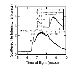
The types of atoms that the He+ beam collides with can be distinguished by determining the TOF (calculated from the distance that the He has traveled), the acceleration voltage and from the weight of the atoms. Figure 6 shows a TOF spectrum for a 3-nm In0.5Ga0.5N single quantum well (SQW) on a GaN film at normal incidence to a He ion beam Reference Sumiya, Nakamura, Chichibu, Mizuno, Furusawa and Yoshimoto[52]. Since the length of travel and the energy of the He ions are 836mm and 2keV, respectively, the TOFs of the He that is backscattered due to collisions with the In and the Ga can be calculated theoretically to be 6417 ns and 6550 ns, respectively. The position of the two sharp peaks in Figure 6 can thus be assigned to the In and Ga signals. TOF spectra with higher mass-resolution for cases where both atoms have atomic weights that are close to each other can be obtained by using Ne ions instead of He ions. The broader TOF spectrum after the Ga signal is attributed to the multiple scattering of He ions. Since the cross-section of light atoms such as nitrogen is smaller, their signals are detected after a longer time-of-flight, and are likely to be in the noise level in Figure 6. An In signal, which is barely detectable, for the 6-nm GaN capped SQW (as indicated in the inset) is probably derived from the interface between the SQW/GaN, due to the channeling effect at normal incidence. This In signal was hardly detectable at other incidence angles. This indicates that CAICISS analysis can detect information from the surface region of III-nitrides, down to a depth of several nm.
TOF spectrum of the backscattered He+ ions used in the CAICISS analysis of an In0.5Ga0.5 SQW when the ion beam was irradiated at normal incidence to the sample. The inset depicts the TOF spectrum for In0.2Ga0.8N capped with 6-nm-thick GaN as a reference [after Reference Ohnishi, Ohtomo, Kawasaki, Takahashi, Yoshimoto and KoinumaRef. 51]. The In and Ga signals can be detected separately for each time-of-flight. The inset indicates how CAICISS analysis detects a region several nm deep below the surface.
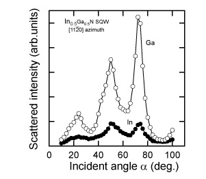
The integrated signal for the III-group element (shadow area in Figure 4) from each TOF spectrum with changing angle of incidence was obtained to evaluate their polarity. Surface contaminants such as C and O, which have small cross-sections, would not have any influence on determining the polarity. Figure 7 shows the angular dependence of the intensities of Ga and In in CAICISS-TOF spectra for an In0.5Ga0.5N SQW. It was confirmed from comparison with the results in Figure 5 that the alloyed In has +c polarity, while the variation in the Ga signal also indicates +c polarity. The indium atoms incorporated into the InxGa1-xN SQW were found to occupy substitutional sites for Ga, and they exhibited +c polarity.
Incident angle dependence of Ga and In scattered intensity at the [11
3. Management of polarity in MBE, PLD, and HVPE-GaN
GaN films are deposited by a variety of growth techniques by different research groups. Reports claiming to show examples of polarity-control are surveyed for each growth technique in this section. Features that are incorporated to control the polarity of GaN are summarized for each of the common growth methods (MBE, PLD and HVPE) with respect to conditions used for treatment of the substrate and/or the LT-buffer layer.
3.1 MBE
Both nitridation of sapphire substrates and deposition under III-rich conditions are considered to be suitable techniques for obtaining high-quality GaN films by MBE. Table II (a) and Table II (b) show a list of research groups, each of which has their own accumulated know-how on growth strategies. Polarity control of MBE-GaN will now be reviewed, focusing on the conditions used for substrate treatment and on the buffer layer technologies that are shown in the Tables.
Relationship between the growth condition and the polarity of GaN deposited on sapphire substrates by MBE. The table shows the list of research groups, each of which has their own know-how on regarding growth.

List of reports claiming polarity conversion from −c to +c MBE-GaN by insertion of a metal layer.

3.1.1. Conditions used for treatment of the sapphire and for the buffer layer
auto Substrate nitridation
Nitridation of the sapphire is carried out by almost all of the research groups. N-radicals generated by an rf plasma are conventionally used for this treatment, which takes place at temperatures ranging from 200 to 1000°C. Sometimes NH3 gas can be used.
Heinlein et al. systematically investigated the time dependence of the nitridation and concluded that it took 200 min of exposure to N-radicals to complete the first monolayer of the surface nitride in an MBE chamber Reference Heinlein, Grepstad, Berge and Riechert[53]. The nitridation done by Mikroulis et al. (Univ. of Crete) at 200°C caused an improvement in the flatness of the sapphire surface and increased the in-plane lattice constant, typically by a value of approximately 9%. The surface become rougher and the lattice constant could be increased by 6.2-6.8% by nitridation at 750°C Reference Mikroulis, Georgakilas, Kostopoulos, Cimalla, Dimakis and Komniou[54]. Namkoong et al. (Georgia Inst. of Tech.) confirmed that 6Å of AlN and 23Å of AlN+NO were formed by nitridation at 200°C and 700°C, respectively Reference Namkoong, Doolittle, Brown, Losurdo, Capezzuto and Bruno[55]. N-radicals are so reactive that they can even nitride the surface of a sapphire substrate at a temperature as low as 200°C. This is completely different from nitridation caused by a flow of NH3 gas, as used in MOCVD (refer to Sec. 4.2). In a technique that is analogous to nitridation in MOCVD, a flow of NH3 gas was introduced into the MBE process by Sonoda et al. (AIST) Reference Sonoda, Shimizu, Shen, Hara and Okumura[56] and Held et al. (Univ. of Minnesota) Reference Held, Nowak, Ishaug, Seutter, Parkhomovsky, Dabiran, Cohen, Grzegory and Porowski[29]. Although the two groups published no results of this surface nitridation technique, Grandjean et al. pointed out that AlN could also be formed by nitridation using an NH3 flow at 850°C for 10 min Reference Grandjean, Massies and Leroux[57].
The polarity of the AlN formed by the nitridation process was suggested to be −c polarity from theoretical calculations done by Felice et al. Reference Di Felice and Northrup[58] (discussed in Sec. 3.1.4). Indeed, it was reported that initial nitridation of the sapphire substrate favors the growth of GaN films along the −c direction Reference Sonoda, Shimizu, Suzuki, Balakrishnan, Sirakashi and Okumura[59].
auto Conditions used for AlN and GaN buffer layers
The polarities of GaN films on non-nitrided sapphire substrates deposited by Dimitrov et al. (Walter Schottky Inst.) using GaN or AlN buffer layers with the same thickness of 15nm were identified as −c or +c, respectively Reference Dimitrov, Murphy, Smart, Schaff, Shealy, Eastman, Ambacher and Stutzmann[60]. In cases such as Piquette et al. (Cal. Inst of Tech. Reference Piquette, Bridger, Beach and McGill[61]) and Namkoong et al. (Georgia Inst. of Tech. Reference Namkoong, Doolittle, Brown, Losurdo, Giangregorio and Bruno[62]) as well as the work of Sonoda et al. (AIST Reference Sonoda, Shimizu, Suzuki, Balakrishnan, Sirakashi and Okumura[59]), MBE-GaN films on nitrided substrate seem to be able to be categorized as +c and −c polarity on AlN and GaN buffer layers, respectively. The polarity seems to be determined by the choice of buffer layer. However, a dependence on the growth conditions has sometimes been observed for both AlN and GaN buffer layers.
The polarity could be systematically varied by changing the thickness of the AlN buffer layer. Dimitorov et al. (Cornell Univ.) demonstrated that the polarity could be controlled from −c to +c polarity (through mixed polarity layers) by using buffer layers corresponding to 0 nm, <5nm, and 5-15nm of AlN Reference Dimitrov, Murphy, Smart, Schaff, Shealy, Eastman, Ambacher and Stutzmann[60]. GaN films on thinner AlN buffer layers (<12nm) are likely to contain IDs, as reported by Georgia Inst. of Tech. Reference Namkoong, Doolittle, Brown, Losurdo, Capezzuto and Bruno[55]. When GaN films are grown not only on sapphire, but also on GaAs (111) B-face substrates, +c polarity can be realized by increasing the thickness of the AlN buffer layer (>20 nm) Reference Hasegawa, Takahashi, Nakayama and Souda[63]. Furthermore, the growth temperature of the AlN buffer layer seems to be important. AlN buffer layers deposited at temperatures higher than those used for depositing HT-GaN layers tend to result in +c polarity, as observed in Georgia Inst. of Tech., the Walter Schottky Inst. and at the Univ. of Minnesota, while the AIST group claim that lower temperatures are more suitable.
Thicker GaN buffer layers lead to +c polarity for MBE-GaN, as reported by Huang et al. Increasing the growth rate of the GaN (increase in the amount of Ga Reference Hughes, Cheng, Novikov, Foxon, Korakakis and Jeffs[64]) also seems to be effective (Virginia Commonwealth Univ.) Reference Huang, Visconti, Jones, Reshchikov, Yun, Baski, King and Morkoc[65]. GaN buffer layers were deposited on NH3-nitrided sapphire by AIST Reference Sonoda, Shimizu, Shen, Hara and Okumura[56] and Univ. of Minnesota Reference Held, Nowak, Ishaug, Seutter, Parkhomovsky, Dabiran, Cohen, Grzegory and Porowski[29]. The polarities determined by the two groups were opposite (the former −c, and the latter +c). In addition, the polarity of MBE-GaN was converted from +c to −c by annealing the GaN buffer layer, as was observed in Univ. of Crete Reference Mikroulis, Georgakilas, Kostopoulos, Cimalla, Dimakis and Komniou[54]. Therefore, the conflict in the use of a GaN buffer layer in MBE was still apparent.
It was very difficult from these papers to find both general conditions that completely covered all of the research groups and any clear relationship between the polarity and the growth conditions. However, we consider through reading many reports that +c GaN would be obtained on an AlN buffer layer deposited under III-rich (higher growth rate) conditions at high temperature in MBE.
auto Insertion of a metal layer
Xu et al. (Chiba Univ.) observed polarity conversion by inserting several Al metal layers onto a −c GaN film after 100 nm of deposition in MBE Reference Xu, Yano, Jia, Yoshikawa and Takahashi[66]. A bi-layer of Al metal was explained as the cause of the converted polarity, and this technique has now been applied to the MOCVD process Reference Lim, Xu, Taniyasu, Suzuki, Arima, Liu, Takahashi and Yoshikawa[67]. Park et al. ((Dongguk Univ.) deposited an Al metal layer directly onto a nitrided sapphire substrate and successfully obtained +c GaN Reference Park, Lee, Ha, Kim, Si, Hwa-Mok, Kang and Oh[68]. Kikuchi et al. (Sophia Univ.) introduced high temperature-grown AlN multiple intermediate layers (HT-AlN-MIL) in migration enhanced epitaxy (MEE), in which Al and N are alternatively supplied into the MBE chamber Reference Kikuchi, Yamada, Kusakabe, Sugihara, Nakamura and Kishino[69]. They controlled the polarity by changing either the number of pairs of HT-AlN-MIL and GaN spacers or the thickness. Yoshida (Furukawa Co. Ltd.) verified the potential of the insertion of Ga metal Reference Yoshida[70] Reference Yoshida and Buturi[71]. Similarly, GaN films can be achieved using a hot wall epitaxy, which consists of the low temperature deposition of Ga metal and subsequent nitridation Reference Ishida, Yamamoto, Ishino, Ito, Fujiyasu and Nakanishi[72]. In addition, we found that M-face GaN could be grown on an Al layer deposited on a sapphire substrate and subsequently nitrided in our MOCVD reactor Reference Okuno, Sumiya and Fuke[73]. Thus, the deposition of a metal layer onto an interface is highly advantageous for controlling orientation, including the polarity of GaN film growth.
3.1.2. Mg accumulation layer
Ramachandran et al. have investigated the phenomenon of Mg adsorption on the surface of a +c GaN layer grown on Si-face 6H-SiC by PAMBE. When the film was exposed to 1.2±0.4ML or more of Mg during growth under Ga-poor conditions, they found that the polarity for the subsequent GaN film switched to −c polarity Reference Ramachandran, Feenstra, Sarney, Salamanca-Riba, Northrup, Romano and Greve[74]. When the inversion takes place, the incorporated Mg concentration in the layer was confirmed to be approximately 8×1019cm−3. At the point where the polarity changed, the interface was rough, with a zigzag inversion domain boundary with mainly {1113} facets and a few (0001) segments Reference Romano, Northrup, Ptak and Myers[75]. Recently, Grandjean et al. have controlled the polarity conversion, not only from +c to −c, but also from −c to +c polarity in NH3-MBE Reference Grandjean, Dussaigne, Pezzagna and Vennegues[76]. The interface in the latter conversion was confirmed as being flat.
A monolayer of Mg deposits on the Ga-terminated surface of the +c GaN film. Since the local structure of the Mg3N2 is more favorable than that of the bulk GaN, the Mg is likely to bond with the N atoms. Consequently, the displacement of the Ga and the N atoms in the outermost layer should occur, forming the configuration Mg-N-Ga/Ga-N from Mg-Ga-N-Ga-N on the +c polar surface. The sign Ga/Ga indicates IDB, consisting of a plane of Ga-Ga bonds. The N atoms are six-fold coordinated with the outermost Mg and the underlying Ga. This surface structure has been theoretically calculated to be the most stable Reference Feenstra, Northrup and Neugebauer[31] Reference Ramachandran, Feenstra, Sarney, Salamanca-Riba, Northrup, Romano and Greve[74]. Recently, a model of pyramidal (zigzag) inversion domains originating from the Mg on the (0001) segment of the boundary was theoretically performed by first-principles pseudopotential density functional calculations Reference Northrup[77]. The most favorable structure of the Mg boundary inserted into the GaN was evaluated as abcab stacking across the (0001) segment, corresponding to the atomic sequence GaNMgNGa, where the side of the boundary lies along the {1113} direction, corresponding to the zigzag inversion domain boundary. In this structure, the concentration of Mg in the boundary layer was calculated to be 3/4 monolayer, occupying H3 sites.
3.1.3. Deposition of GaN film: V/III ratio and growth rate
Tarsa et al. deposited GaN films homo-epitaxially on +c GaN templates by plasma-assisted MBE Reference Tarsa, Heying, Wu, Fini, DenBaars and Speck[78]. GaN films deposited with a low V/III ratio (Ga-stable) had a quality comparable with the underlying GaN template, while GaN films with a high V/III ratio (N-stable) showed a faceted surface and poor crystalline quality. Held et al. Reference Held, Crawford, Johnston, Dabiran and Cohen[79] and Myers et al. Reference Myers, Hirsch, Romano and Richards-Babb[80] deposited on −c GaN templates by MBE. The former obtained GaN films with 3-D growth under excess NH3 (Ga-limited growth) and films with a step-flow growth under excess Ga (NH3-limited growth). The latter obtained GaN samples with pyramidal hillocks or a flat surface morphology under N- and Ga-stable conditions, respectively. The Ga-rich condition is likely to result in GaN films with a smooth surface, regardless of the polarity of the template.
The dependence of the polarity on growth rate is also observed for GaN and AlN buffer layers, shown in Table II (a), as well as in ZnO films with the same wurtzite crystal structure Reference Ohkubo, Ohtomo, Ohnishi, Matsumoto, Koinuma and Kawasaki[81]. Takahashi et al. deposited GaN films on GaAs (111) A and B-face substrates by MOMBE. The deposition was carried out at 700°C by changing the Ga flux (beam equivalent pressure (BEP); 2~8×10⁻⁸Torr) under a constant supply of DMHy as the N source. The growth rate of the GaN on both substrates increased up to 5×10⁻⁸Torr of Ga supply, and then saturated at 400nm/h above that level. This indicates that the growth was promoted with a supply-limit (N-rich) for the lower BEP, while it occurred with a surface kinetic limit (Ga-rich) for the higher BEP. GaN films on A-face GaAs (111) were found to have +c polarity, and were independent of the growth rate. On the other hand, the polarity on the GaAs (111) B-face was −c for the supply-limited condition, and it was +c when it was kinetic-limited. GaN grown under III-rich conditions (kinetic limited, Ga- stable or limited growth) is considered to predominantly display +c polarity Reference Takahashi, Nakayama, Souda and Hasegawa[82].
3.1.4. Factors for controlling the polarity in MBE-GaN on sapphire substrate
The following are considered to be the key points that are decisive in determining the polarity of MBE-GaN;
-
1. Use of an AlN buffer layer deposited on a sapphire substrate at higher temperature with a higher growth rate (III-rich conditions)
-
2. Insertion of an Mg, Al and Ga metal layer at the interface
-
3. Use of a thicker LT-GaN buffer layer.
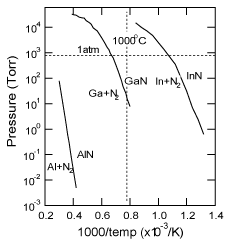
The vapor pressure of GaN is much higher than that of AlN, as shown in Figure 8 Reference Edgar, Strite, Akasaki, Amano and Wetzel[83]. AlN buffer layers, with their lower vapor pressure, should be suitable to act as nucleation layers for MBE-GaN grown under high vacuum conditions. Felice et al. calculated theoretically the atomic structure of films consisting of approximately 1 bilayer of AlN on c-plane sapphire substrates Reference Di Felice and Northrup[58]. Under equilibrium conditions, the Al layer in the H3 sites lying between the last O plane (blue region) and the first N plane (yellow region) maintain the stoichiometry of bulk sapphire for 2/3 monolayers, as shown in Figure 9 (a) and Figure 9(b). This favorable structure could be changed by the amount of Al in the initial growth, from Al-rich in Figure 9 (a) to Al-poor in Figure 9 (b). Both of the geometries of the AlN on the outermost layer (between the green brackets) corresponded to +c polarities (from previous calculations) Reference Northrup, Di Felice and Neugebauer[84]. In contrast, the alignment of the AlN (between the red brackets) in Figure 9(c) and Figure 9(d) corresponded to −c polarity. This structural difference is observed in the complete interface of Al adatoms lying in the T4 sites between the last O plane and the N plane. The calculations predicted that the polarity of these very thin films on sapphire substrates would be attributed to that of the III-V nitrides. Moreover, since the two structures in Figure 9 (b) and Figure 9 (c) have very similar formation energies, independent of Al abundance, it is assumed that a slight fluctuation in conditions in the initial stages of deposition can alternately switch the structure. The situation that is shown in Figure 9 (c) must occur under non-equilibrium conditions, such as nitridation of the sapphire under Al-deficient conditions. Consequently, the nitridation of sapphire is regarded as resulting in −c GaN, though moderate nitridation as carried out by the AIST group Reference Sonoda, Shimizu, Shen, Hara and Okumura[56] might form the interface structure shown in Figure 9 (b). Increasing the supply of group III implies that the growth of nitride materials would approach the equilibrium state, forming the structures with +c polarity shown in Figure 9 (a) and Figure 9 (b).
Equilibrium N2 pressure over III-V nitrides (solid) + III-metal (liquid). Lines for each nitride material are plotted together from Ref. Reference Ohkubo, Ohtomo, Ohnishi, Matsumoto, Koinuma and Kawasaki81
Models for the AlN thin films on c-plane sapphire substrates given in Ref. Reference Di Felice and Northrup[58]. The color regions are added to explain the theoretical predictions. The structures in the brackets correspond to the polar structures of AlN described in Ref. Reference Northrup, Di Felice and Neugebauer[84]. (a) and (b) correspond to a +c polar surface. (c) and (d) to −c polarity.

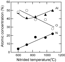
Nitridation-temperature dependence of the atomic concentration on a sapphire surface determined by XPS analysis. When HT-GaN films were deposited on sapphire substrates nitrided at temperatures of more than 700°C, the films represented −c polarity and hexagonal facetted surfaces.
3.2 PLD
In the pulsed laser deposition (PLD) technique, III-nitride films are fabricated in an N2 ambient through the deposition of precursors that are ablated from a metal target or from nitride powder by an intense pulsed excimer or Nd:YAG laser. Since the use of PLD makes it possible to lower the substrate temperature, various substrates can be used in PLD Reference Dispute, Wu, Jagannadham and Narayan[85] Reference Ohta, Fujioka and Ohsima[86].
The orientation of GaN films deposited by PLD was GaN [11
3.3 HVPE
HVPE has mainly been used in order to fabricate bulk or free-standing GaN with lower threading dislocations on MOCVD-GaN templates patterned with SiO2 Reference Usui, Sunakawa, Sakai and Yamaguchi[91] or W Reference Kawaguchi, Nambu, Sone, Yamaguchi, Miyake, Hiramatsu, Sawaki, Iyechika and Maeda[92] masks. Smooth HVPE-GaN was obtained by the insertion of a ZnO layer on a sapphire substrate. This GaN was confirmed to be +c polarity, as demonstrated by Romano et al. Reference Romano, Northrup and O’Keefe[20] in Sec. 2.1. The initial growth on the substrate seems to be also important in HVPE. In this section, the conditions for HVPE-GaN deposition on substrates without a GaN template are summarized in terms of surface morphology (polarity), as in Sec. 3.1 for MBE.
3.3.1. Until 1992: Direct growth, GaCl treatment, and ZnO insertion
The first GaN film was deposited on a sapphire substrate by HVPE in '69 Reference Maruska and Tietjen[93]. Judging from its hexagonal-facetted surface morphology, this GaN film had −c polarity. Intensive efforts have been made to grow smooth large area HVPE-GaN films directly on sapphire substrates by Monemar et al. Reference Monemar, Lagerstedt and Gislason[94].
In Table III, reports of GaN growth on sapphire substrates by HVPE are listed with respect to the relationship between initial growth conditions and surface morphology. The first smooth HVPE-GaN was achieved by Naniwae et al. in 1990 Reference Naniwae, Itoh, Amano, Itoh, Hiramatsu and Akasaki[95]. The key technology was the treatment of the sapphire substrate by Ga+HCl at 1030°C. In order to obtain smooth GaN, Ga+HCl treatment should be carried out for more than 20min, as shown in the Table. Two years later, Detchprochm et al. found that the insertion of a ZnO layer on the sapphire substrate made it possible to grow HVPE-GaN that was transparent, with a smooth surface Reference Detchprochm, Hiramatsu, Amano and Akasaki[96]. A 10-300nm thick ZnO buffer layer was deposited on the sapphire substrate by sputtering at room temperature, and then the sapphire substrate that was covered with the ZnO layer was introduced into the HVPE system.
GaN samples grown on sapphire substrates by HVPE. Relationship between surface morphology and the initial growth on the substrate is summarized.

The vapor pressure of ZnO is so high at 1000°C in an HVPE reactor that there was no evidence of ZnO at the GaN/sapphire interface, as reported by Molnar et al. Reference Molnar, Götz, Romano and Johnson[97]. Ga atoms left on the sapphire by the GaCl treatment should be desorbed as well. However, it is supposed that a very small fraction of the Zn or the Ga could form compositions that would play a role in converting the polarity at the interface of the sapphire.
3.3.2. 1997-1999: AlN and GaN buffer layers
AlN and GaN buffer layers began to be used in 1997. The effectiveness of AlN buffer layers was confirmed by Lee et al. for the first time Reference Lee, Yuri, Ueda, Harris and Sin[98]. Paskova et al. made a comparison of the effects of sapphire nitridation, GaCl treatment and AlN buffer layers for HVPE-GaN growth Reference Paskova, Birch, Tungasmita, Becard, Heuken, Svedberg, Runesson, Goldys and Monemar[99]. (The growth of AlN buffer layers was carried out by sputtering in a separate apparatus due to the AlCl3 corroding the quartz tube of the HVPE reactor). It was concluded that the smoothest GaN was achieved by the use of an AlN buffer layer.
Wagner et al. reported that HVPE-GaN grown on a GaN buffer layer was smoother than that on an AlN buffer layer deposited by MOCVD Reference Wagner, Parillaud, Buhlmann and Ilegems[100]. Here, it is worth noting that HVPE-GaN on an LT-GaN buffer layer less than 10nm thick had a hexagonal-facetted surface (discussed in Sec. 4.3 Recipe 1-(2)). The GaN buffer layer could be desorbed during the ramping of the substrate temperature under an NH3 ambient, and then the unintentional direct-growth of HVPE-GaN on the sapphire substrate was supposed to take place. In contrast, smooth HVPE-GaN was deposited on AlN buffer layers. This is why AlN buffer layers, which have a lower desorption rate (as shown in Figure 8) were expected to work as nucleation layers even at the high temperatures used for HVPE-GaN growth.
The importance of variations in the LT-buffer layer caused by annealing can be found in the report by Tavernier et al., who applied a similar buffer layer technology to that used in MOCVD to HVPE in a single chamber Reference Tavernier, Etzkorn, Wang and Clarke[101]. Their studies of buffer layers revealed that layer thickness and annealing conditions are crucial to obtaining HVPE-GaN of high quality.
3.3.3. 2000-2003: Kinetic effect and a new approach
Small islands that were typically several nm in height were formed on sapphire substrates by the nitridation treatments used in HVPE Reference Gu, Zhang, Shi, Zheng, Zhang, Dwikusuma and Kuech[102] and in MOCVD. Nitridation of the substrate is likely to result in −c GaN growth with hexagonal-facetted surfaces, as discussed in the section on MBE-GaN. However, such a trend is not observed in HVPE-GaN. Namerikawa et al. reported that +c polarity was observed for HVPE-GaN samples deposited on both A- and B- face GaAs (111) substrates Reference Namerikawa, Sato, Takahashi, Suemasu and Hasegawa[103]. This is probably due to the use of growth rates as high as a few μm/min. (Murakami et al. found that when an LT-GaN buffer layer on a B-face substrate was annealed in an NH3 ambient, the substrate was deteriorated due to etching of the buffer layer, suggesting that GaAs (111) B-face substrates are not suitable for GaN deposition Reference Murakami, Kumagai, Seki and Koukitsu[104].)
In HVPE-GaN, the coalescence of the GaN islands occurs rapidly (within 10 sec of their growth) corresponding to 0.4-0.5μm of film thickness Reference Golan, Wu, Speck, Vaudo and Phanse[105]. The quality of the HVPE-GaN can be divided into two regimes, thinner than 0.4-0.5μm and thicker than that, which correspond to destructive and better quality, respectively. Gu et al. obtained better quality HVPE-GaN by changing the optimum conditions for the two regions Reference Gu, Zhang, Shi, Zheng, Zhang, Dwikusuma and Kuech[102]. In addition, in a similar way to the case of MEE Reference Kikuchi, Yamada, Kusakabe, Sugihara, Nakamura and Kishino[69] given in Sec. 3.1, flow modulated growth (FMG) with a periodically interrupted HCl flow under a constant flow of NH3 can also improve HVPE-GaN, as reported by Zhang et al. Reference Zhang, Riemann, Alves, Heuken, Meister, Kriegseis, Hofmann, Christen, Krost and Meyer[106].
3.3.4. Features for controlling polarity in HVPE-GaN
Nitridation of the sapphire substrates in HVPE does not have a great influence on the surface morphology (polarity) of the GaN, probably due to the high growth rate induced by the kinetic effect. However, the interface compositions between the substrate and the initial very thin film are crucial to +c polarity, as provided in the following:
-
1. GaCl treatment of the sapphire substrate
-
2. Deposition of ZnO and AlN layers in an isolated system
-
3. Use of a thicker LT-GaN buffer layer.
These features are supposed to be essentially equal to those used in MBE. In order to understand the general context of polarity control beyond these growth techniques, it will be necessary to be able to analyze a sapphire surface treated with GaCl and also these buffer layers.
4. Polarity management in MOCVD-GaN
An LT-buffer layer is indispensable, not only for growing high-quality HT-GaN films, but also for controlling their polarity, as observed in the drastic improvements in surface morphology that have been achieved since 1986. The quality of the LT-buffer layer strongly depends on the substrate treatment, the growth conditions and the subsequent annealing. The dependencies of the LT-buffer layer on these conditions are highlighted by our studies (detailed below) under Articles,where we attempt to understand the implications of the various conditions. In the subsequent sections, entitled The Recipes, we propose methods that would lead to control of the polarity.
4.1 Previous work
A few years after the development of AlN and GaN buffer layers, LEDs based on III-nitride materials were realized by the MOCVD process. Device development has always been more advanced in research into MOCVD-GaN. Therefore, know-how for improving GaN materials has not always been reported as often as it might have been. As far as we could determine during our survey, the number of reports claiming polarity-control in MOCVD-GaN are far fewer than those for MBE-GaN. Polarity issues in MOCVD-GaN seem to have been left behind. There are, however, some reports that detail how the optimization of the growth conditions for each of the processes in MOCVD happened to result in changes in the polarity and/or the surface morphology.
The first GaN films deposited by MOCVD in 1984 had hexagonal-facetted Reference Kawabata, Matsuda and Koide[107] or granular surfaces Reference Hashimoto, Amano, Sawaki and Akasaki[108]. By using an LT-AlN buffer layer, GaN with a smooth surface was achieved for the first time in 1986 Reference Amano, Sawaki, Akasaki and Toyoda[1]. It has been thought that this variation could be related to the polarity. Hwang et al. investigated the influence of sapphire nitridation on GaN films in 1995 Reference Hwang, Schurman, Mayo, Li, Lu, Liu, Salagaj and Stall[109]. Their nitridation was carried out at 900°C for 5min. GaN films using 50nm of LT-GaN buffer layer deposited on nitrided and non-nitrided sapphire substrates had hexagonal-facetted or smooth surfaces, respectively. The carrier density for GaN films on nitrided sapphire was higher by one order of magnitude than that for films on non-nitrided substrates. In addition, the mobility of the former was 1/4 of that of the latter. That is, the substrate nitridation not only had an influence on the surface morphology, but also on the properties of the GaN. Van Der Stricht et al. systematically changed the surface morphology of GaN films deposited on nitrided sapphire substrates from hexagonal-facetted to smooth by lowering the deposition temperature of the GaN buffer layer from 550 to 450°C Reference Van Der Stricht, Moerman, Demeester, Crawley, Thrush, Middleton, Trager-Cowan and O’Donnell[110]. The variations (re-crystallization or sublimation Reference Estes Wickenden, Wickenden and Kistenmacher[111] Reference Ramer, Zheng, Kranenberg, Banas and Hersee[112]) of the LT-buffer layer induced by the gas ambient Reference Han, Ng, Biefeld, Crawford and Follstaedt[113] and the annealing time Reference Lin, Chi, Feng, Guo, Tsang and Hong[114] Reference Sugiura, Itaya, Nishio, Fujimoto and Kokubun[115] were investigated intensively to improve the quality of GaN films. Thus, the key technologies for controlling the polarity in MOCVD can usually be found in thesis reports. The implications of these conditions will be discussed with respect to polarity-control in the subsequent sections.
4.2 Our sample conditions in MOCVD
Our GaN films have been grown conventionally on c-plane sapphire substrates using LT-buffer layers by a two-step sequence in an atmospheric pressure MOCVD apparatus with a vertical water-cooled quartz reactor. Trimethyl-gallium (TMG), trimethyl-aluminum (TMA) and NH3 gases were used as the Ga, Al and N source materials, respectively. H2 and N2 were used as the carrier gases. A quartz inner tube was used in order to enhance the flow velocity of the source gases arriving on the substrate on a graphite susceptor. The MOCVD process involves the following steps; substrate treatment [cleaning in flowing H2 at 1000°C and/or nitridation], deposition of an LT-buffer layer, ramping up the substrate temperature (annealing of the buffer layer) and deposition of the high-temperature (HT) GaN film. LT-GaN or AlN buffer layers were used in our studies. Table summarizes the typical growth conditions.
Although the conditions can be independently controlled during each process step, each step has an influence on the subsequent processes. There are infinite combinations of conditions until deposition of the HT-GaN film. The polarities of samples prepared under a representative condition for each process were analyzed by each of CAICISS, X-TEM and chemical stability.
4.3 Substrate treatment and GaN buffer layer
4.3.1. Article 1: Surface of the treated sapphire substrate
It is most important to recognize that the surface of the substrate is the first hetero-interface in GaN film growth. The surface of the sapphire substrate was investigated using XPS when the substrate was treated by cleaning under H2 or by nitridation under flowing NH3.
Although the surface of the sapphire substrate was sometimes covered with undesirable contamination (Ga, N, Al, Si etc.) due to hysteresis in the MOCVD apparatus Reference Golan, Fini, DenBaars and Speck[116], oxygen was conventionally removed from the sapphire surface during H2 cleaning. Consequently, the surface was slightly rougher, and an Al-rich surface was formed, which was confirmed to be Al:O = 50:50% by XPS. When it was subsequently nitrided under flowing NH3 at various temperatures between 600°C and 1080°C, the surface compositions of the Al, O and N were changed, as shown in Fig. 10 . Nitrogen was detected for sapphire nitrided at even 600°C, and the nitrogen composition increased with higher temperature, while the oxygen decreased.
Thus, an Al-rich surface was formed on the sapphire substrate by the removal of oxygen during H2 cleaning. In contrast, AlOxN1−x was induced by nitridation, depending on the temperature used. These chemical states at the surface of the substrate play a decisive role in the polar structure of the buffer layer and also the evaporation behavior. (Refer to Recipes 1 and 2).
4.3.2. Article 2: Structure of the LT-GaN buffer layer on the nitrided sapphire substrate
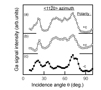
To understand the correlation between the MOCVD-process and the polarity, it is necessary to evaluate the polarity of the LT-buffer layer itself. Figure 11 shows CAICISS results for LT-GaN buffer layers on H2-cleaned and nitrided sapphire substrates Reference Sumiya, Tanaka, Ohtsuka, Fuke, Ohnishi, Ohkubo, Yoshimoto, Koinuma and Kawasaki[36] Reference Sumiya, Ohnishi, Tanaka, Ohtomo, Kawasaki, Yoshimoto, Koinuma, Ohtsuka and Fuke[117]. The dependence of the intensity on the incident angle shows less variation due to the poor crystalline quality of the buffer layer (refer to Sec. 2.4). However, the dominant polarity of buffer layers as thin as 20nm can be judged from these results by comparison with the results in Figure 5. There are two interesting features observed from this result. Firstly, both as-deposited buffer layers show +c polarity, independent of the substrate treatment. The other is that the resulting polarity for the layer on the nitrided sapphire was converted to −c polarity after the annealing, while the polarity was +c for the film on the H2 cleaned substrate.
Angular dependence of Ga signal intensity for the buffer layers in CAICISS analysis: (a) as-deposited 20-nm buffer layer on non-nitrided sapphire, (b) as-deposited 20-nm buffer layer on nitirided sapphire and (C) annealed buffer layer of (b). The polarity of a buffer layers on nitrided sapphire substrates changed from +c to −c polarity, while there was no change for buffer layers on non-nitrided sapphire substrates. [after Reference Sumiya, Ohnishi, Teshigawara, Tanaka, Ohkubo, Kawasaki, Yoshimoto, Ohtsuka, Koinuma and FukeRef. 35]. This is the first determination of the polarity for LT-GaN buffer layers, which has led to an understanding of the correlation between the MOCVD process and the polarity.
Our concern was focused on buffer layers on nitrided sapphire. The non-stoichiometric AlOxN1−x layer formed by the nitridation is likely to have −c polarity, as indicated by theoretical calculations Reference Di Felice and Northrup[58]. Both +c and −c polarity nucleate simultaneously on the nitrided sapphire, probably due to either inhomogeneous nitridation Reference Sumiya, Ohnishi, Tanaka, Ohtomo, Kawasaki, Yoshimoto, Koinuma, Ohtsuka and Fuke[117] or favorable formation energy. The surface of the as-deposited buffer layer would be covered with a +c layer with higher growth rate Reference Yamane, Shimada, Endo and DiSalvo[118]. Subsequent annealing of the film would make the −c domains rise to the surface due to the sublimation of the film. Based on these considerations, buffer layers on nitrided sapphire substrate are assumed to be covered with a +c layer grown laterally over the −c domains.
To confirm this assumption, thicker buffer layers (210nm) were prepared on nitrided sapphire and annealed for various times at 1040°C. An LT-GaN buffer layer on a nitrided substrate was found to evaporate with a layer-by-layer mode due to the AlOxN1−x on its surface Reference Sumiya, Ogusu, Yotsuda, Itoh, Fuke, Nakamura, Mochizuki, Sano, Kamiyama, Amano and Akasaki[119]. Figure 12 shows the angular dependence of the Ga signal intensity in CAICISS for the thicker buffer layer annealed for 0, 10, 20 and 30min Reference Sumiya, Yoshimura, Ogusu, Fuke, Mizuno, Yoshimoto and Romano[120]. The CAICISS result for the as-deposited sample shows predominantly +c polarity [Figure 12 (a)]. The sample continues to have +c polarity after annealing for 10min. Sharpening of the peaks is also observed in the result, suggesting an improvement in the crystal quality near the surface [Figure 12 (b)]. The peak at 72° splits into two peaks and the peak at 35° intensifies with further annealing, as shown in Figs. 12 (c) and (d). This indicates that the film surface is transforming from +c polarity (triangles) to −c polarity (squares). The lines in Figs. 12 (c) and (d) present the weight ratio of +c: −c polarity at 5:5 and 2:8, respectively, with the assumption that they share the same crystal quality (i.e., the same intensity of the CAICISSS signal for +c and −c domains).
Incident angular dependence of Ga signal intensity at [11
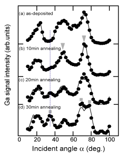
Since CAICISS analysis detects the atomic arrangement of only the surface region (as discussed in Sec. 2.4), the films were further investigated by TEM Reference Sumiya, Yoshimura, Ogusu, Fuke, Mizuno, Yoshimoto and Romano[120]. Figure 13 shows X-TEM images for the same samples that are shown in Figs. 12 (c) and 12 (d). Columnar IDs were found to extend to the surface, and dome-shaped domains were found near the interface, similar to the observations reported by Wu et al. Reference Wu, Brown, Kapolnek, Keller, Keller, DenBaars and Speck[121]. With increasing annealing time (sublimation of the film), the dome-shaped domains are exposed to the surface. The TEM images are consistent with the CAICISS spectra. Since the −c signal component of the CAICISS result increased after annealing, the inverted domains (dome shaped) can be considered to have −c polarity.
Cross-sectional TEM images for the buffer layers annealed for (a) 20min and (b) 30min. The samples correspond to (c) and (d) in Figure 12, respectively. [after Reference Yamane, Shimada, Endo and DiSalvoRef. 118]

4.3.3. Article 3: Interface between the GaN buffer and the treated sapphire substrate
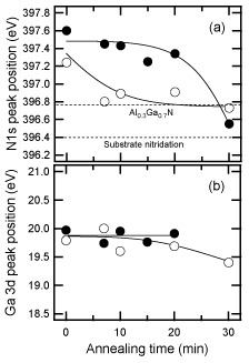
The interface between the GaN buffer layer and the substrate was investigated by XPS. Figure 14 shows the annealing-time dependence of the peak position of N1s for buffer layers on both H2 cleaned and nitrided sapphire substrates. The peak positions for both as-deposited layers are observed at around 397.4 eV, corresponding to GaN. The sample on nitrided substrate mostly evaporated after annealing for 20min, because the position of N 1s at 396.5eV, corresponding to the AlN and Ga signals, was in the noise level. In contrast, AlxGa1−xN was formed at the interface between the GaN buffer layer and the H2 cleaned sapphire substrate. The peak position for the annealed buffer layer on the H2 cleaned sapphire stayed at 396.8eV, regardless of the time, and the Ga 3d peak was shifted to slightly lower binding energy from GaN (19.8eV) Reference Sumiya, Ogusu, Yotsuda, Itoh, Fuke, Nakamura, Mochizuki, Sano, Kamiyama, Amano and Akasaki[119].
Dependence of (a) N1s and (b) Ga 3d peak positions for a 20-nm-thickness GaN buffer layer on H2 cleaned (open circles) and nitrided (closed circles) sapphire substrates on the annealing time under the N2 and H2 mixed ambient. The positions were detected by XPS analysis. [after Reference Sumiya, Ohnishi, Tanaka, Ohtomo, Kawasaki, Yoshimoto, Koinuma, Ohtsuka and FukeRef. 117] The sample on the nitrided substrate evaporated completely, and AlGaN was formed at the interface between the sample and the non-nitrided substrate.
Recently, we have deposited a GaN film by MOCVD on an H2 cleaned sapphire substrate that had once been exposed to air. Although the surface should have been terminated with oxygen, a +c GaN film with sufficient quality was obtained on the sapphire by two-step MOCVD without the need for a second H2 cleaning process [122]. The sapphire surface becomes rougher by H2 cleaning, represented by the weak RHEED pattern. In addition, a comparable GaN film with high quality was even grown on a sapphire substrate cleaned in an N2 ambient at more than 1000°C Reference Sato, Ogawa, Ohtsuka, Kuwahara, Sumiya, Takano and Fuke[123]. It is supposed from these facts that the thermal roughening of sapphire at higher temperature might be important as a nucleation site for the growth of the LT-buffer layer.
4.3.4. Recipe 1: Thickness and annealing of the GaN buffer layer on nitrided substrates
Taking into account the IDs structure of the GaN buffer layer on the nitrided sapphire reported in Article 2, we demonstrate how to control the polarity of the HT-GaN by changing the thickness of the buffer layers and the conditions used for the annealing. The mixed polarity of the buffer layers grown by MBE on nitrided sapphire has also been observed by CAICISS analysis Reference Sonoda, Shimizu, Suzuki, Balakrishnan, Sirakashi and Okumura[59]. Since GaN film growth on nitrided sapphire substrates is supposed to be similar to growth by MBE, our recipes in MOCVD will be compared with the features found in MBE, which are listed in Table II (a) and Table II (b).
auto Thickness
Thicker buffer layers (160nm) were deposited and annealed for various times at 1040°C under a gas ambient of NH3: H2: N2 = 750:750:500sccm. The absorbance at 3.6eV decreases as a function of the annealing time, as shown Figure 15 (a), indicating a reduction in the thickness. Their polarities, as determined by CAICISS, are indicated in the figure. GaN films were deposited on these annealed buffer layers, with their polarities clearly identified. GaN films with smooth (+c) and hexagonal faceted (−c) surfaces were confirmed when deposited on thicker buffer layers annealed for 10min (+c) and more than 30min (−c), respectively. The size of the hexagonal facets could be systematically changed up to 60μm by varying the annealing time of the buffer layer, as shown in Figure 15 (b). We suppose that the milky surface of the GaN film was probably due to +c and −c mixed growth Reference Sumiya, Tanaka, Ohtsuka, Fuke, Ohnishi, Ohkubo, Yoshimoto, Koinuma and Kawasaki[36].
(a) Dependence of absorbance at 3.6eV on annealing time for a 160nm GaN buffer layer on a nitrided sapphire substrate. (b) Variation of hexagonal facet size of GaN films deposited on annealed buffer layers in (a). The polarities of the HT-GaN layers are attributed to those of the annealed buffer layers. [after Reference Sumiya, Ohnishi, Teshigawara, Tanaka, Ohkubo, Kawasaki, Yoshimoto, Ohtsuka, Koinuma and FukeRef. 35]

The effect of the thickness of the buffer layer can be seen in the data for MBE-GaN films shown in Table II (a). In spite of the presence of an AlN or GaN buffer layer, MBE-GaN films on thicker buffer layers are likely to have +c polarity. When the group at Georgia Inst. of Tech. Reference Namkoong, Doolittle, Brown, Losurdo, Giangregorio and Bruno[62] increased the thickness of the AlN from 12 nm to 30 nm, the polarity was converted from mixed polarity to +c polarity. Similar results were obtained by both the Virginia Commonwealth University, who used GaN buffer layers more than 60 nm thick Reference Huang, Visconti, Jones, Reshchikov, Yun, Baski, King and Morkoc[65] and the Walter Schottky Institute, who used AlN buffer layers that were more than 5 nm in thickness Reference Dimitrov, Murphy, Smart, Schaff, Shealy, Eastman, Ambacher and Stutzmann[60]. These examples of polarity conversion depending on the thickness of the buffer layer are exactly similar to our case for MOCVD-GaN.
auto V/III ratio
GaN buffer layers were deposited on nitrided sapphire under Ga-rich (lower V/III ratio: 2000) and optimized (V/III ratio: 20 000) conditions. Figure 16 shows AFM images for 20-min annealed buffer layers deposited under (a) optimum and (b) Ga-rich conditions before (on the left) and after (on the right) dipping them in KOH solution. The smooth surface of the optimum buffer layer turned into a rough surface, indicating −c polarity. In contrast, the surface for the Ga-rich buffer layer is resistant to the KOH solution, indicating +c polarity Reference Weyher, Müller, Grzegory and Porowski[32]. From these results, the III-rich condition might be considered to suppress the effect of −c polarity on nitrided sapphire substrates.
AFM images of annealed buffer layers on nitrided sapphire substrates before (on the left) and after (on the right) dipping in KOH solution for each time stated. (a) The sample deposited under a V/III ration of 20 000 and annealed in the H2 and N2 mixed ambient for 20min, and (b) the sample deposited under a V/III ratio of 5000 and annealed in an N2 ambient for 20min. [after Reference Sumiya, Ohnishi, Tanaka, Ohtomo, Kawasaki, Yoshimoto, Koinuma, Ohtsuka and FukeRef. 117]

The FWHM of the Ga 3d spectrum detected by XPS for the former as-deposited sample was 2.2 eV wider than that (1.5-1.7eV by our analysis) for the latter layers Reference Sumiya, Ogusu, Yotsuda, Itoh, Fuke, Nakamura, Mochizuki, Sano, Kamiyama, Amano and Akasaki[119], suggesting the existence of Ga metal or Ga that was weakly bonded with the N. Thus, the III-rich condition is suggested as being effective for obtaining a +c interface, as discussed in section 3.1.4 for MBE, as well as in MOCVD. Furthermore, the effect of the III-rich condition on the +c polarity might be extended to the HVPE technique using the GaCl treatment mentioned in Sec. 3.3.
auto Annealing conditions for the buffer layer
The Ga-rich buffer layer is supposed to predominantly cohere and/or evaporate during the initial annealing. In fact, we confirmed that the buffer layer had completely evaporated within 7 min under an ambient of NH3: H2:N2 = 750: 750: 500 sccm. The sublimation could be suppressed by increasing in the amount of N2 (replacing the H2) in the gas ambient, and this annealed buffer then worked as a nucleation layer.
The annealing of the LT-buffer layer in MOCVD is a unique process. To add to the importance of the V/III ratio, the annealing conditions are also crucial to the polarity in terms of controlling the thickness of the buffer layer. An H2 ambient should be used for thicker or III-poor buffer layers, while an N2 ambient is appropriate for a thin or III-rich layer in order to obtain a buffer layer of the optimum thickness. These correlations are very complex, depending on the individual growth apparatus. Our case is referred to in detail elsewhere Reference Sumiya, Ogusu, Yotsuda, Itoh, Fuke, Nakamura, Mochizuki, Sano, Kamiyama, Amano and Akasaki[119].
Two recipes for obtaining +c GaN on nitrided sapphire are; 1) the deposition of a thicker buffer layer under III-rich conditions, and 2) annealing of the layer for a short time under an N2 ambient. We suppose that Uchida et al. in Ref. 4, who deposited +c GaN on nitrided sapphire substrates, managed to use these correlations in their MOCVD apparatus.
4.3.5. Recipe 2: Growth on H2 cleaned substrates
H2 cleaning of sapphire substrates is indispensable for the growth of GaN with a smooth surface by two-step MOCVD. GaN films and GaN buffer layers on this type of substrate have +c polarity. The basis of the recipe for preventing growth with −c polarity on H2 cleaned sapphire is in preventing the substrate from undergoing unintentional nitridation.
It was confirmed that nitridation using NH3 gas at temperatures higher than 700°C resulted in −c GaN films in our deposition system. In addition, the introduction of a flow of NH3 into the reactor, even for several seconds at 1080°C, resulted in the growth of −c GaN films. Therefore, unintentional nitridation probably takes place in the following circumstances; 1) when NH3 is introduced into the reactor during the decrease in substrate temperature for the deposition of the LT-buffer layer after H2 cleaning of the sapphire, and 2) when a longer time is used and annealing is carried out in an H2 ambient for a thin LT buffer layer (exposure of the sapphire surface). These factors indicate the importance of correct timing of the switching of the source gases when shifting to a subsequent part of the growth process.
Seelmann-Eggebert et al. have already pointed out that the occurrence of inversion domains in the films could mainly be attributed to poor process control during substrate cleaning and in the very initial stages of the nucleation process, preceding buffer growth Reference Seelmann-Eggebert, Weyher, Obloh, Zimmermann, Rar and Porowski[6]. It is supposed that the GaN with the hexagonal facets on a thin buffer layer that was reported in Ref. Reference Nakamura[3] might originate from the unintentional nitridation of the sapphire substrate.
4.4 AlN buffer layer
4.4.1. Article 4: Comparison with LT-GaN buffer layers
Figure 17 shows the dependence on annealing time of the XRD intensity of the (0002) peaks of 20 nm thick LT-GaN and AlN buffer layers deposited on H2 cleaned sapphire at 600°C under optimum conditions. Since the thermal annealing caused the crystallization of the buffer layer Reference Amano, Akasaki and Buturi[124], the intensity of the GaN (0002) diffraction was enhanced when it was annealed for 10 min. The extended annealing caused the layer to be thinner due to sublimation. It is worth noting here that it took double the time for the AlN to achieve maximum intensity in Figure 17, probably due to the lower mass-transportation and sublimation of the AlN buffer layer. This implies that the annealing conditions should be changed to suit the kind of buffer layer used Reference Kobayashi, Akasaka and Kobayashi[125] Reference Ito, Sumiya, Takano, Ohtsuka and Fuke[126]. Indeed, the ω (0002) FWHM of GaN on an AlN buffer was improved from 400 (10 min annealing, which was the optimum time for the GaN buffer layer) to 240 arcsec, simply by annealing the AlN buffer for a longer time (20 min), as shown in Figure 17.
Variation of (0002) peak intensity of LT-GaN (open circles) and AlN (closed circles) buffer layers of 20nm thickness as a function of annealing time. The intensity was enhanced due to the crystallization of the samples induced by the annealing, and it subsequently decreased due to the layer being thinned by sublimation. This indicates that the effects of mass transportation and sublimation are smaller for AlN buffer layers.
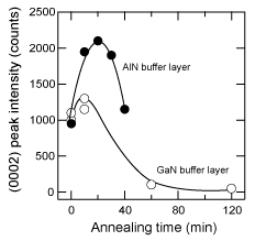
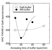
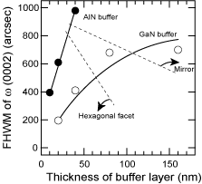
Figure 18 shows the relationship between the FWHM and the annealing time for 20 nm thick AlN and GaN buffer layers. The annealing time means the time interval from the end of the buffer layer deposition at 600°C till the start of the HT-GaN deposition at 1040°C. After taking 7 min to reach 1040°C, the annealing was maintained at 1040°C for the remainder of the time. All of the samples exhibited +c polarity. Although the best quality GaN was obtained on an AlN buffer layer, the values changed drastically in the narrow window of the annealing-time conditions. Figure 19 shows the FWHM and surface morphology (polarity) of HT-GaN films on nitrided sapphire substrates using AlN and GaN buffer layers of various thicknesses. The buffer layers were annealed for 10min. As discussed in Recipe 1, the material changed from −c to +c polarity (through a mixed polarity condition) for both types of buffer layer with increasing buffer layer thickness. However, the window for the AlN buffer layer is narrower, as in the case shown in Figure 18. Therefore, LT-GaN buffer layers may have an advantage for controlling the polarity of GaN films grown by MOCVD.
FWHM of ω (0002) for HT-GaN films deposited on GaN (open circles) and AlN (closed circles) buffer layers with the same thickness, when the buffer layers were annealed for the times shown in the figure. The conditions for obtaining better quality HT-GaN material are wider with GaN buffer layers Reference Ito, Ohtsuka, Kuwahara, Sumiya, Takano and Fuke[127]].
The FWHM value of ω (0002) for 1 μm HT-GaN films deposited on AlN (closed circles) and GaN (open circles) buffer layers with the thicknesses in the figure. The buffer layers were annealed for 10min under the optimum ambient. Their polarity changed as indicated by the surface morphology, and the polarity conversion occurred drastically in the case of the AlN buffer layer.
4.4.2. Recipe 3: High-temperature AlN buffer layers
HT-AlN buffer layers are useful in the growth of GaN films by MBE (Table II (a) in Sec. 3.1). When an HT-AlN buffer layer was deposited at 1040°C in MOCVD, introducing NH3 at high temperature caused the unintentional nitridation of the sapphire (Recipe 2). Consequently, the GaN films had −c polarity with hexagonal facets. Two experiments have been undertaken to prevent this conversion to −c polarity when using an HT-AlN buffer layer Reference Ito, Ohtsuka, Kuwahara, Sumiya, Takano and Fuke[127].
The TMA precursor was introduced into the reactor 10 seconds before the NH3 gas during the deposition of an HT-AlN buffer layer at 1040°C. As expected, a +c GaN film was achieved. Judging from the deposition rate, the thickness of the Al metal layer was estimated to be 4 Å during this 10 second period. In another experiment, a lower V/III ratio of less than 1800 was used for the AlN deposition at 1040°C, which resulted in +c GaN with a smooth surface, as shown in Figure 20. These two recipes, 1) the deposition of Al metal and 2) the use of a lower V/III ratio, seem to be consistent with the features seen in MBE.
Influence on surface morphology of HT-GaN films of the V/III ratio in AlN buffer layers deposited at 1040 °C; V/III ratio= (a) 600, (b) 1800, (c) 6800, and (d) 13700. Reference Ito, Ohtsuka, Kuwahara, Sumiya, Takano and Fuke[127] ] A lower V/III ratio was required for the deposition of AlN buffer layer in order to obtain +c GaN film.

4.5 Polarity of the HT-GaN
4.5.1. Article 5: Correlation between the polarity and the growth process
The polarity of HT-GaN was found to be attributable to that of the annealed buffer layer from the observations in the previous sections. During re-growth on a GaN template, the polarity could also attributed to that of the template, as recognized by Weyher et al. Reference Weyher, Brown, Zauner, Muller, Boothroyd, Foord, Hageman, Humphreys, Larsen, Grezegory and Porowski[128]. In our deposition system, the deposition rate of MOCVD-GaN films is limited by the arrival rate of the TMG source gas. Films are grown with changing deposition rates, ranging from 0.9 to 5.0 μm/h. The polarities of these MOCVD-GaN films were identical with those of the annealed buffer layer on nitrided sapphire substrates Reference Sumiya, Yoshimura, Ito, Ohtsuka, Fuke, Mizuno, Yoshimoto, Koinuma, Ohtomo and Kawasaki[129]. This is inconsistent with MBE-GaN in terms of the kinetic effect highlighted in Sec. 3.1.3. Although the range of conditions used for the HT-GaN might be insufficient, we insist here that the polar structure at the interface of one of the underlying layers (the annealed LT-buffer layer or the template) would be the most crucial factor in determining the polarity of GaN films in MOCVD.
We have investigated the implications in the exact growth sequence and conditions in MOCVD. When summarizing them in Articles 1-5 and Recipes 1-3with respect to the polarity, the relationship between the growth conditions and the polarity can be represented as a branching road map on a timing chart of the MOCVD process, as shown in Figure 21 Reference Sumiya and Fuke[130]. The route is divided by the nitridation of the sapphire substrate. In order to achieve +c GaN in MOCVD, the sapphire substrate must not be nitrided after the H2 cleaning. In the case where nitridation occurs, however, the polarity can still be controlled by modifying the preparation of the LT-buffer layer.
Summary of the key points for controlling the polarity of GaN films on sapphire substrates (as detailed in the Articles and the Recipes) in the time chart of the two-step MOCVD process. Our typical growth conditions are represented. The polarity at the end of each process is remarked with blue and red indicating +c and −c polarity, respectively, which can be used as the road map to control the polarity of GaN in MOCVD. [after Reference Weyher, Brown, Zauner, Muller, Boothroyd, Foord, Hageman, Humphreys, Larsen, Grezegory and PorowskiRef. 128]

4.5.2. Recipe 4: Application of the road map
The road map can be examined in several ways, not just for controlling the polarity, but also for depositing GaN films on various substrates. When GaN films are deposited on Si-face 6H-SiC substrates in MOCVD, it is well known that LT-AlN buffer layers should be used. When an LT-GaN buffer layer was used, part of the SiC surface was exposed during the time that the temperature was ramping because of the absence of a non-volatile intermediate layer (such as AlGaN) at the interface of the sapphire substrates (Article 3). To overcome this unsuitable feature of using an LT-GaN buffer layer on a SiC substrate, it was annealed in an N2 ambient to suppress evaporation during the ramping of the temperature (Recipe 1(3)). As expected, a GaN film with a smooth surface and of better quality was obtained on the SiC substrate using the LT-GaN buffer layer Reference Kurumasa, Ito, Ohtsuka, Kuwahara, Sumiya, Takano and Fuke[131].
By modifying the timing of the introduction of the source gases according to Recipe 2, growth of GaN was achieved on a Si (111) substrate using only an AlN buffer layer. The key point of this was that the TMA and the NH3 gas should arrive simultaneously at the Si substrate in order to prevent the Al and N from alloying with the Si Reference Matsuura, Ochi, Sumiya and Fuke[132].
GaN films were deposited on (La0.29, Sr0.71)(Al0.65, Ta0.35) O3 (LSAT) (111) substrates, which have a lattice constant that corresponds to the 3×3 structure of GaN (0001) and a thermal expansion coefficient close to that of GaN. Since the LSAT substrate was deteriorated by NH3 and TMG gases at high temperature, an AlN layer was used as a blocking layer to protect the surface. The GaN film on the LSAT had +c polarity and its GaN [1
5. Polarity dependence of properties and device performance
The focus of our concern moves on to the polarity-dependence of the properties of GaN films and device performance. Morkoc et al. Reference Morkoc, Di Carlo and Cingolani[135] have already reviewed the band profile and the characteristics of electronic devices such as field effect transistors, considering the spontaneous and piezoelectric polarizations. The systematic variations of the 2DEG density and the band profile for an AlGaN /GaN / AlGaN hetero-structure were theoretically predicted by Ambacher et al., taking into account the thickness of the barrier layer, the composition of the ternary alloy, the degree of strain, and the screening of the polarization field by free carriers Reference Ambacher, Smart, Shealy, Weimann, Chu, Murphy, Schaff, Eastman, Dimitrov, Wittmer, Stutzmann, Rieger and Hilsenbeck[136].
In this section, the polarity-dependence of the optical properties of GaN films is discussed with respect to impurity-incorporation and defect formation. Furthermore, the structures of interfaces are summarized with respect to the contact formed between the metal and GaN polar surface, which are not fully discussed in these excellent reviews.
5.1 Optical properties and defect formation
Figure 22 shows depth profiles of +c and −c GaN films. The yields of the matrix ions of Ga and GaN- are constant throughout the films. Comparing the results for both GaN films, C, O, and Al impurities are incorporated by one or two orders of magnitude more into −c GaN, while Si impurities have an incorporation rate that is several times higher into +c GaN Reference Sumiya, Yoshimura, Ohtsuka and Fuke[137]. Consistent with the higher level of impurities, the carrier concentration for −c GaN was much higher than that for +c GaN, in spite of the growth conditions (the V/III ratio) and the growth rate. The dependence of the impurity incorporation can be explained either by the difference in the adsorption energy between the matrix elements and the impurities on the polar surface Reference Zywietz, Neugebauer and Scheffler[138] or by differences in the mode of the growth.
Depth profiles of C-, O-, Al-, Si-, Ga- and GaN- for (a) +c GaN and (b) −c GaN films of 1μm in thickness. The intensities of impurities normalized to the GaN- count are listed at the bottom of each figure. The values normalized to the Ga+Ga+ ion in the brackets are evaluated from depth profiles using and O2 + primary beam [after Reference Morkoc, Di Carlo and CingolaniRef. 135]. The Al, C and O impurities were more readily incorporated into −c GaN films.

Li et al. found that the doping behavior of Mg and the resulting conductivity of the doped layers in MBE-GaN strongly depends on the polarity of the GaN Reference Li, Jukovic, Wang, Van Hove and Chow[139]. In fact, Mg was incorporated by up to a factor of 30 times more into +c GaN Reference Ptak, Myers, Romano, Van de Walle and Northrup[140]. Activation of the p-type dopants was achieved for +c GaN. One of the reasons why this was possible is thought to be that C and O impurities are incorporated more into −c GaN Reference Ng and Cho[141]. GaN films on bulk GaN single crystals with −c polarity grown by MOCVD Reference Frayssinet, Knap, Prystawko, Leszczynski, Grezegory, Suski, Beaumount and Gibart[142] and films on ZnO with O-face polarity grown by MBE Reference Hellman, Buchanan, Wiesmann and Brener[143] were also found to contain more oxygen impurities in the −c GaN, respectively, which was confirmed by IR and SIMS. This impurity-dependence on the polarity is consistent with our experiments with MOCVD-GaN, except for the case of Si Reference Sumiya, Yoshimura, Ohtsuka and Fuke[137]. Comparable Si incorporation into both types of GaN films has been suggested by both Ng et al. and ourselves, while Li et al. reported higher incorporation of Si in −c GaN. The issue of Si impurity incorporation is still therefore controversial.
The dependence of impurity incorporation on the polarity resulted in differences in the IR Reference Frayssinet, Knap, Prystawko, Leszczynski, Grezegory, Suski, Beaumount and Gibart[142] and Raman spectra Reference Cros, Joshi, Smith, Cantarero, Martines-Criado, Ambacher and Stutzmann[41] as in Sec. 2.1. The dependence of the optical properties and of defect formation on the polarity was investigated on our +c and −c GaN films. The PL spectrum of +c GaN at 8K Reference Chichibu, Setoguchi, Uedono, Yoshimura and Sumiya[144] exhibits free A and B exciton emission [FE(A) and FE(B)] at 3.492 and 3.499eV, respectively, as shown in Figure 23 (a). The recombination of the first excited states of the A exciton [FE(An=2)] is also found at 3.510eV. These assignments are based on the position of the energies of the respective exciton absorption peaks. The sample also exhibits exciton recombination at 3.486 and 3.464 eV, which are due to the bound-to-neutral donor (D0, X) and neutral deep acceptor (A0 d, X) transitions, respectively. The PL peak at 300K is assigned to the free exciton emission, as revealed from Figure 23 (c). Conversely, −c GaN exhibits a rather broader PL band and an absorption tail, as in Figure 23 (b) and (d). The spectrum at 8K exhibits a peak at 3.475eV and a shoulder around 3.45 eV. Since the residual electron density of the −c GaN is as high as 3.5×1018cm−3, the disappearance of excitonic absorption due to Coulomb screening by the increase in temperature above 75K is reasonable. However, −c GaN exhibits a Stokes shift of nearly 20 meV at 300K, although high quality Si-doped +c GaN (with nearly the same electron density of 2.2 x1018cm−3) did not show any Stokes shift at 300K. Therefore, the formation of an impurity-induced band tail is probable in −c GaN, which subsequently causes band gap narrowing due to potential fluctuations and inhomogeneous distribution of the fixed charges. The donor impurity is considered to be O, which is more readily incorporated into −c GaN, as revealed by SIMS in Figure 22. To determine the possibility for the incorporation of acceptor-type defects such as Ga vacancies Reference Gorczyca, Svane and Christensen[145], mono-energetic slow positron annihilation measurements were carried out. Indeed, the S parameter of −c GaN Reference Uedono, Chichibu, Chen, Sumiya, Suzuki, Ohdaira, Mikado, Mukai and Nakamura[146] is greater than that of +c GaN, as shown in Figure 24. The fitting results of the relationship between E and S are also shown by the solid lines, and the diffusion lengths of positrons are derived to be 23nm for +c GaN and 4.8nm for −c GaN. These results imply that −c GaN contains a higher density of vacancy-type defects or defect-complexes than +c GaN. Therefore, the formation of extended band-tail states in −c GaN is considered to be due to the simultaneous distribution of donors and acceptor-type vacancy defects, which occurred during the growth of the −c polarity GaN material.
Comparison of PL and OA spectra at 8K and 300K for +c and −c GaN films. [after Reference Frayssinet, Knap, Prystawko, Leszczynski, Grezegory, Suski, Beaumount and GibartRef. 142]

The line shape parameter S of +c and −c GaN as a function of the position of the acceleration energy E. The value of S depends on the size and density of vacancy-type defects. The diffusion length of positrons decreases with increasing defect density. [after Reference Frayssinet, Knap, Prystawko, Leszczynski, Grezegory, Suski, Beaumount and GibartRef. 142]

5.2 Schottky barrier
Karrer et al. characterized the influence of the polarity on the electrical properties (I-V and C-V measurements) of Pt Schottky diodes on Si-doped epitaxial GaN layers with +c and −c polarity Reference Karrer, Ambacher and Stutzmann[8]. An effective Schottky barrier height (SBH) was measured between Pt/GaN by using the I-V characteristics as a function of the ideality factor. The value of the SBH was determined to be 1.1 and 0.9 eV for devices on +c and −c GaN with the same carrier density (ne=6−10×1017cm−3) respectively. Jang et al. also reported that the SBH determined by I-V characteristics on +c GaN (ne=3×1016cm−3) was higher by 0.31 eV than that on −c GaN (ne=1×1017cm−3) Reference Jang, Lee and Lee[44], which was consistent with Karrer's report in terms of the difference in the SBH. However, the SBH values measured by C-V were 1.75 eV for the +c GaN and 0.85 eV for −c GaN (Karrer et al). Furthermore, the energy of the valence-band edge for the +c GaN surface was higher by 1.4 eV than that for −c GaN measured by high resolution photoemission spectroscopy (HRPES). There are large differences in the SBH of GaN diodes obtained from C-V and I-V measurements. Since these Pt/GaN samples were prepared on GaN deposited by the MBE method, inversion domains (IDs) containing −c polarity should exist in the +c GaN. A small fraction of −c IDs with lower barrier height may be regarded as a reason for large difference in the results between the I-V and the C-V measurements. Since a larger diode current may be selectively injected into −c IDs, the SBH can be underestimated from the measured I-V characteristics. On the other hand, since the ratio of the areas of the two domains contributes to the SBH determined by the C-V measurement, a small quantity of −c IDs would hardly have any influence on the result.
Rickert et al. studied the SBH for thin metal over-layers of Au, Al, Ni, Ti, Pt and Pd on n- and p-type +c GaN samples using synchrotron radiation-based x-ray photoemission spectroscopy Reference Rickert, Ellis, Kim, Lee, Himpsel, Dwikusuma and Kuech[147]. Figure 25 shows the values of the SBH of the six kinds of metals as a function of the work function of the metals. The relationship between the SBH and the work function did not obey the perfect Schottky barrier model. The change in the barrier height was smaller than the value expected from the change in the metal work function. These results indicate the importance of the effect of the surface state and the interface state (refer to Sec. 5.4). To explain this appropriately, a model that takes into account the pinning of the Fermi level at the surface would be required. The position of the Fermi level on the surface of the GaN can be changed by the kind of metal, the conduction type of the GaN, or the chemical treatment of the surface. In addition, the SBH for a Pt/n-GaN structure was reported to be about 1.6 eV, which is comparable to that obtained by C-V measurement and HRPES.
Surface barrier heights measured in Ref. Reference Rickert, Ellis, Kim, Lee, Himpsel, Dwikusuma and Kuech[147] for n-GaN shown as a function of the work function of the metal used for the contact formation.

Surface barrier heights measured in Ref. Reference Rickert, Ellis, Kim, Lee, Himpsel, Dwikusuma and Kuech[147] for p-GaN shown as a function of the work function of the metal used for the contact formation.

5.3 Ohmic contact
The formation of ohmic contacts has been achieved on many semiconductors by either high impurity doping in the contact region or by decreasing the tunneling barrier thickness at the metal / semiconductor interface. In the case of nitride semiconductors, the formation of an ohmic contact can be expected owing to the polarization effect.
Jang et al. compared the characteristics of an ohmic contact using Ti/Al/Ni/Au metal on +c GaN with that on a −c GaN sample Reference Jang, Lee and Lee[44]. The contact resistivities, as determined by the transfer length method (TLM), were 8.3×10⁻⁴Ωcm2 for the +c sample and 7.0×10⁻²Ωcm2 for the −c sample. These samples were annealed at 700°C for 1 min. Although the net carrier concentration of the −c sample was higher than that of +c sample, the contact resistivity on the +c GaN was lower by two orders of magnitude than that on the −c GaN.
It is well known that a thin AlN layer can be formed at the interface between the metal and the GaN after annealing a Ti/Al contact at a temperature higher than 400°C. Luther et al. explained the lower contact resistivity for a +c sample as being due to polarization, that is, a 2DEG could be induced by polarization at the +c AlN/GaN interface, but not at the −c interface Reference Luther, DeLucca, Mohney and Karlicek[148]. Therefore, the effective SBH for the tunneling probability of an electron through the AlN epilayer in a +c sample is considered to be much higher than that for a −c sample. Kwak et al. investigated the effects of polarity on the electrical properties of Ti/Al contacts for n-type GaN Reference Kwak, Lee, Han, Cho, Chae, Nam and Park[149]. They reported that Ti/Al contacts on n-type +c GaN become ohmic with a contact resistivity of 5×10⁻⁵Ω cm2, while a Schottky contact with a barrier height of over 1 eV was formed for contacts on n-type −c GaN.
The effects of polarity on ohmic contacts to p-type GaN were also investigated. Band bending, which is caused by the polarization charge of a thin InGaN capping layer on a p-GaN layer, is utilized to realize the ohmic contact. Gessmann et al. discussed the effect of thin strained cap layers on the contact resistance of p-type +c GaN Reference Gessmann, Li, Waldron, Graff and Schubert[150] Reference Gessmann, Graff, Li, Waldron and Schubert[151]. Two cases were investigated; a GaN cap/AlGaN structure and an InGaN cap/GaN structure. The electric field in the strained cap layers can reduce the thickness of the tunneling barrier at the metal/semiconductor interface. Since band bending due to the capping layer can be induced by an internal electric field, the thickness of the capping layer must be optimized so that two conditions, the formation of the 2DEG and sufficient tunneling probability for holes, could be satisfied simultaneously. The specific contact resistances were obtained experimentally using the TLM-method. These were 6×10⁻³Ω cm2 for InGaN (2nm) /p-GaN (Ni/Au contact: annealing at 500°C) and 7×10⁻⁴ Ω cm2 for GaN (10nm)/AlGaN (Pd/Au contact: annealing at 500°C). These results indicated the advantageous effect of polarization fields in the cap layer on the reduction of ohmic contact resistance.
5.4 Surface state
Surface or interface states are probably not taken into account in the analysis of the experimental data mentioned in Sec. 5.3 and 5.4. In addition, the surface state density has seldom been taken into consideration in theoretical calculations of the band structure. However, Ridley estimated the electron populations induced by spontaneous and piezoelectric polarization in n-type +c AlGaN/GaN hetero-structures by using elementary electrostatic theory Reference Ridley[152]. He considered several points, such as the existence of the donor density in the barrier layer, the surface charge (adsorbed ion and surface state population change) of the GaN buffer layer and/or the AlGaN barrier layer. It is suggested that the thickness of the surface barrier layer should be optimized according to the pinning position of the Fermi level by the surface states, though the 2DEG density induced at the hetero-interface must become larger with increasing thickness of the barrier layer.
Several methods of reducing the surface states have been proposed. The treatment with (NH4)2Sx carried out by Lin et al. Reference Lin, Wang and Chang[153] caused the band bending of a p-type +c GaN surface to release by 0.25eV. The interface states of an n-type +c GaN surface were decreased to 1×1012 cm−2eV−1 by treatment with an N2 plasma, which was about 1/5 of the level for a non-treated surface (experiment carried out by Hashizume et al. Reference Hashizume and Nakazaki[154]). Furthermore, a decrease in the electron affinity of Cs-adsorbed AlN Reference Wu and Khan[155] and GaN Reference Wu and Khan[156] surfaces was observed due to the effect of the Cs-surface dipole, which was formed by an initial interaction between the Cs and the empty surface states. Unfortunately, these experimental data were not discussed in connection with spontaneous polarization, which induced sheet charges. Although a method of controlling the surface states has not yet been established, the control of charges caused by surface states and spontaneous polarization is considered to be one of the new topics that could realize new functionality from nitride semiconductors.
6. Summary and Remarks
The evaluation and control of crystalline polarity are important because the spontaneous and piezoelectric polarizations are large enough to influence the band-profile of hetero-structures in the III-nitride system (Sec. 2). These polarizations can be used not only for controlling the SBH and achieving ohmic contacts (Sec. 5.2 to 5.4), but also for exploring new functionalities in III-nitrides (Sec. 5.5). Taking it into account that impurities (O, C, and Al) and vacancy-type defects (VGa) are more readily incorporated into −c GaN films (Sec. 5.1), it is necessary to grow +c GaN films with smooth surfaces.
GaN films grown by MBE, PLD, HVPE and MOCVD have been reviewed, mainly with respect to the control of polarity. The first three are based on the published literature, while the last is based on our studies. Focusing on the growth conditions in the substrate treatment and/or the preparation of LT-buffer layers, a set of conditions for obtaining +c GaN films is provided for each growth method, as follows;
-
(1). MBE and PLD (Sec. 3.1 and 3.2)
-
a) Use an AlN buffer layer deposited on a sapphire substrate at higher temperature under a higher growth rate (III-rich condition)
-
b) Insertion of Mg, Al and Ga metal layers at the interface
-
c) Use of a thicker GaN buffer layer.
-
-
(2) HVPE (Sec. 3.3)
-
a) GaCl treatment of the sapphire substrate
-
b) Deposition of ZnO and AlN layers in an isolated system
-
c) Use of a thicker LT-GaN buffer layer.
-
-
(3) MOCVD (Sec. 4)
-
a) Prevent H2 cleaned sapphire substrates from undergoing unintentional nitridation.
-
b) Use thicker LT-GaN buffer layers deposited under a lower V/III ratio on nitrided sapphire substrates.
-
c) Much lower V/ III ratio for HT-AlN buffer layers on sapphire substrates.
-
A III-rich condition at the interface of the sapphire substrate is mostly decisive in the disparate growth techniques. Indeed, the III-rich condition (lower V/III ratio) has been used during the deposition of LT-buffer layers on H2-cleaned sapphire substrates in our MOCVD. The initial growth at the interface of the sapphire under the III-rich condition should occur in an equilibrium state leading to +c polarity, though the kinetic effect is still unclear.
CAICISS can be used to evaluate the polarity of thin films such as buffer layers (Sec. 2.4). The polarity of an LT-buffer layer was detected for the first time by using CAICISS (Sec. 4.3). We have studied the role of the LT-buffer layer and its implications in each process for GaN film growth by two-step MOCVD, not only in terms of controlling the polarity but also for improving material quality. A road map representing the correlation between the polarity and the growth conditions in MOCVD has been made, as shown in Figure 21. Indeed, the polarity can be managed from +c to −c though mixed polarity by systematically varying the conditions used in MOCVD-GaN. Although the initial growth on sapphire would determine the polarity of the epitaxial materials, the polarity can be controlled by understanding the structure of the LT-buffer layer and its implications for the MOCVD process. It can be concluded through these studies that the polar structure at the interface of an annealed LT-buffer layer is the most crucial factor in determining the polarity of a GaN film.
Recently, the importance of polarity was highlighted in the state-of-the-art growth of InN films Reference Nanishi, Saito and Yamaguchi[157] Reference Xu and Yoshikawa[158], and-c GaN with a smooth surface has apparently been obtained by MOCVD Reference Matsuoka[159]. Moreover, we have discovered that an HNO3 treatment of H2-cleaned sapphire substrates resulted in −c GaN film growth in MOCVD Reference Takabe, Sumiya and Fuke[160]. Thus, even more interesting results relating to film polarity have been reported. We intend to further promote studies of the polarity of III-nitrides for applications that utilize the effects of polarity.
Acknowledgments
The authors would like to thank the students who have been working in our laboratory for conducting their experiments. We would like to express special thanks to Dr. Ohnishi (Univ. of Tokyo) for his intense collaborations in CAICISS analysis, and for his valuable discussions. We gratefully acknowledge collaborations from Mr. Mizuno and Mr. Furusawa for CAICISS analysis of InGaN SQWs, for Dr. Chichibu for his optical measurements, for Dr. Uedono for his positron annihilation measurements and for Dr. Romano for her X-TEM observations. We are grateful to many collaborators who have supported and encouraged our research. This work was supported by a Grant-in-Aid for Developmental Scientific Research (No. 14703024) and by the Asahi Glass Research Foundation.


