

1. Introduction
GaN is typically grown epitaxially on lattice-mismatched substrates, since large-area GaN wafers are not available Reference Strite and Morkoç[1]. The most commonly used substrate is Al2O3, but its 13.8% lattice mismatch with GaN can lead to very poor interface characteristics. A partial solution to this problem involves low-temperature growth of a thin GaN or AlN buffer layer between the Al2O3 and the main GaN layer, and this technique works well for layers grown by metal-organic chemical vapor deposition (MOCVD) or by molecular-beam epitaxy (MBE). On the other hand, buffer layers are typically not employed in hydride vapor-phase epitaxy (HVPE), although sometimes the Al2O3 is pretreated with ZnO before the GaN growth Reference Molnar, Nichols, Maki, Brown and Melngailis[2]. Whatever the case, reports indicate that the HVPE growth process always leads to a thin, highly conductive interface region, which is not only detrimental to certain devices, but which also obscures the bulk electrical properties Reference Look and Molnar[3]. This problem is of practical importance, because it appears that thick HVPE GaN layers, separated from their Al2O3 substrates, are becoming a material of choice for GaN homoepitaxy Reference Oh, Lee, Park, Lee, Song and Han[4] Reference Reynolds, Look, Jogai, Saxler, Park and Hahn[5]. Thus, it is essential to develop techniques to isolate the bulk electrical properties from those near the interface. Here we show how differential Hall-effect (D-H) measurements can be used for that purpose, and we compare D-H results with those achieved by a much simpler method, presented previously.
2. Two-layer Model
Roughly speaking, we can model HVPE GaN samples as being composed of a bulk region with thickness db, mobility μb, and carrier concentration nb, and a thin interface region, with similar parameters di, μi and ni. (In this study, we will deal with Hall mobilities and Hall concentrations. The connections with conductivity mobilities and the true concentrations, respectively, are well known Reference Look[6].) The overall mobility μ and sheet carrier concentration ns will then be given by Reference Look and Molnar[3] Reference Look[6]


Clearly, it is impossible to determine all four quantities μb, μi, nb, and ni from measurements of μ and ns alone. However, the interface layer is always (in our experience) composed of degenerate electrons, and if the bulk layer contains nondegenerate electrons, then the bulk electrons will freeze out at very low temperatures, and the interface electrons will become dominant. (In some cases, the interface electrons are dominant at all temperatures.) Moreover, if the interface electrons are degenerate, they are also temperature-independent (easily verified during the course of the experiment), so that the values of μi and nis (=nidi) measured at low temperatures can be inserted into Equation (1) and Equation (2) at all temperatures, and the values of μb and nb thus determined. (Usually, db >> di, so that db ≈ d, the total layer thickness.) This method, designated “B-I” (“bulk/interface”) here, was introduced earlier Reference Look and Molnar[3], and has also been applied by other groups in the analysis of HVPE GaN/Al2O3 layers. However, the assumption that μi and ni are constant at all temperatures has never been proven. In the present study, we have explicitly etched off a total of more than 5 μm, leaving mainly the interface region, and have thus been able to measure the temperature dependence of μb and nb. We also can compare the B-I method with the more accurate (in principle) D-H technique, described below.
3. Differential Hall-effect Model
The D-H method requires removal of a thin layer δd, and measurement of μ and n both before and after the removal. Then, the values of μ and n within the layer δd can be deduced from Equation (1) and Equation (2):


In our case, the layer δd was removed by reactive-ion etching (RIE), using a BCl3/Cl2/Ar plasma. However, in order to be able to get accurate measurements of δd, a small (25-μm x 25-μm) hole was first milled into the middle of the sample by using a focused ion (Ga) beam. A schematic, cross-sectional view of the resulting sample configuration is shown in Figure 1. It was verified by Hall/van der Pauw measurements on the unetched sample that adding the hole had little effect on the values of μ and n. Also, since our RIE recipe does not attack Al2O3, the substrate surface exposed at the bottom of the hole served as a fiduciary point for the subsequent thickness measurements done after each etch. Thicknesses were determined with a stylus profiler or atomic force microscope. Unfortunately, because of the very strong interface conductance in this sample, it was necessary to remove at least 1 μm at each step, in order to get a reasonable signal-to-noise ratio. However, for layers grown by MBE or MOCVD, there is usually no conductive interface layer, and so the D-H resolution should be much better for these layers.
A schematic, cross-sectional diagram showing a GaN/Al2O3 layer with a small hole used for thickness measurements.

4. Results and Discussion
The results are shown in Figure 2. In this figure, the Al2O3/GaN interface is at depth = 0. The sample was etched to a minimum value of 0.75 μm, and at this thickness the interface is totally dominant. Thus, the data points shown at 0.75/2 μm result from simply measuring the μ and n of this final layer, and then assigning the values to the midpoint of the layer. In contrast, the μ and n data points shown at other depths result from the D-H process, as described above. As seen, n correlates quite well with the [O] profile, as determined from secondary-ion mass spectroscopy (SIMS) [7], and in fact, the sheet concentration of [O] is within a factor two of the sheet concentration of n in this interface region, clearly showing that O is a shallow donor. Furthermore, the value of n in the rest of the layer correlates well with the [O] + [Si] profiles, especially when compensation is taken into account. That is, we would expect that n ≤ ND − NA ≈ [O] + [Si] − NA < [O] + [Si], where ND and NA are the donor and acceptor concentrations, respectively. As expected, n < [O] + [Si] everywhere except for the point nearest the interface, which is not as accurate anyway. Note also that [Si] > [O] for d > 0.5 μm. This observation is in agreement with SIMS measurements in thick samples (d ≥ 10 μm) Reference Look, Stutz, Molnar, Saarinen and Liliental-Weber[8], which find only Si near the surface. Thus, in the present samples, Si is the dominant donor in the bulk region, and O in the interface region. To complete the compensation picture, positron-annihilation data have earlier been used to show that the Ga vacancy is the dominant acceptor in all regions Reference Look, Stutz, Molnar, Saarinen and Liliental-Weber[8].
Profiles of mobility μ, carrier concentration n, O concentration [O], and Si concentration [Si] in a GaN/Al2O3 layer grown by HVPE. The interface is at depth = 0.

Note that the 300-K mobility near the surface has a value of about 1000 cm2/V-s, denoting very good material. The standard (one-layer) Hall analysis gives only about 200 cm2/V-s, because of the interface influence. Thus, it is critical to correct the Hall results on HVPE layers.
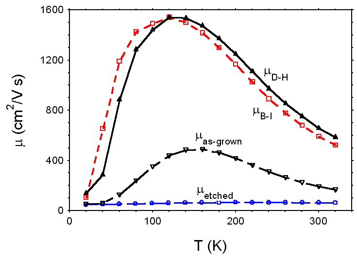
We now compare the D-H analysis of the top 5 μm, using Equation (3) and Equation (4) (δd = 5 μm), with the more convenient B-I analysis presented earlier, in which the whole sample is simply split into “interface” and “bulk” regions, with the interface μ and n being taken as those measured at 20 K. Again, the assumption is that the bulk electrons will be frozen out at 20 K, so that μ20K = μi and n20K = ni, and also that μi and ni are independent of temperature. The temperature-dependent mobilities and carrier concentrations of the as-grown sample (d = 5.9 μm) and the etched sample (d = 0.75 μm) are shown in Figure 3 and Figure 4, respectively. We note that μetched and netched are nearly temperature-independent over the whole range, showing that the interface electrical parameters are indeed degenerate. We also note that μetched = μas-grown at 20 K, showing that the bulk/interface division is reasonable in the as-grown sample. (In Figure 4, it appears that netched ≠ nas-grown at 20 K; however, the “sheet” concentrations of these respective quantities are indeed equal.)
Temperature dependences of the (apparent) mobility μas-grown of an as-grown GaN/Al2O3 layer, about 6-μm thick, and the (apparent) mobility μetched of the same layer etched to a thickness of 0.75 μm. Also shown are μD-H, which is the average mobility of the top 5 μm, as determined by differential-Hall measurements, and μB-I, which is the average mobility of the “bulk” region (also approximately the top 5 μm), calculated by correcting μas-grown for the degenerate interface layer.
Temperature dependences of the (apparent) carrier concentration nas-grown of an as-grown GaN/Al2O3 layer, about 6-μm thick, and the (apparent) carrier concentration netched of the same layer etched to a thickness of 0.75 μm. Also shown are nD-H, which is the average carrier concentration of the top 5 μm, as determined by differential-Hall measurements, and nB-I, which is the average carrier concentration of the “bulk” region (also approximately the top 5 μm), calculated by correcting μas-grown for the degenerate interface layer.

If we apply the B-I method Reference Look and Molnar[3], then Equation (1) and Equation (2) give the curves μB-Iand nB-Iin Figure 3 and Figure 4, respectively. On the other hand, if we employ the more accurate D-H technique, then μD-H and nD-H result. Clearly, the simpler B-I method is satisfactory, especially for T > 100 K. Thus, the etching process is not necessary for the determination of the average μ and n in the top 5 μm (the “bulk” region, in this case). However, the D-H method is indeed necessary for accurate results in the near-surface region.
5. Conclusions
In conclusion, we have determined mobility and carrier concentration profiles in a 6-μm-thick HVPE GaN layer grown on Al2O3. The carrier concentration profile closely mimics the [O] + [Si] profile, proving, among other things, that O is a shallow donor. The near-surface mobility is about 1000 cm2/V-s, much higher than the average value, about 200 cm2/V-s, which is strongly influenced by the interface region. For “bulk” values only (the top 5 μm, in this case), a much simpler technique, introduced earlier, suffices.
ACKNOWLEDGMENTS
We wish to thank R.J. Molnar for the GaN sample, T. A. Cooper for the Hall-effect measurements, and P.D. Cassity for the RIE processing. D.C.L. and J.E.H. were supported under AFRL Contract F33615-00-C-5402, and AFOSR Grant F49620-00-1-0347.


