Introduction
It has been a necessity for investigators in the III-nitride community to grow films of GaN and related nitride materials using heteroepitaxial growth routes because of the dearth of bulk substrates of these materials. This results in films containing dislocation densities of 108-1010 cm−2 because of the mismatches in the lattice parameters and the coefficients of thermal expansion between the buffer layer and the film and/or the buffer layer and the substrate. These high concentrations of dislocations may also limit the performance of devices.
Several groups [Reference Kapolnek, Keller, Vetury, Underwood, Kozodoy, Denbaars and Mishra2-Reference Zhong, Johnson, McNulty, Brown, Cook and Schetzina10], including the present authors, have conducted research regarding selective area growth (SAG) and lateral epitaxial overgrowth (LEO) techniques for GaN deposition, specifically to reduce significantly the dislocation density. Increased emphasis in this research topic was fueled in part by the announcement by Nakamura, et al. [Reference Nakamura, Senoh, Nagahama, Iwasa, Yamanda, Matsushita, Kiyoku, Sugimoto, Kozaki, Umemoto, Sano and Chocho11-Reference Nakamura, Senoh, Nagahama, Iwasa, Yamanda, Matsushita, Kiyoku, Sugimoto, Kozaki, Umemoto, Sano and Chocho13] of the dramatic increase in projected lifetime of their GaN- based blue lightemitting laser diodes fabricated on LEO material. Using these approaches, researchers have been able to grow GaN films containing dislocation densities of ≈ 105 cm−2 in the areas of overgrowth.
However, to benefit from this reduction in defects, the placement of devices incorporating LEO technology is limited and confined to regions on the final GaN device layer that are located on the overgrown regions.
Recently we have pioneered a new approach to selective epitaxy of GaN and AlxGa1−xN layers, namely, pendeo- (from the Latin: to hang or be suspended) epitaxy (PE) [1,Reference Zheleva, Smith, Thomson, Linthicum, Gerhke, Rajagopal and Davis14-Reference Zheleva, Thomson, Smith, Rajagopal, Linthicum, Gehrke and Davis19] as a promising new process route leading to a single, continuous, large area layer; multilayer heterostructures or discrete platforms of these materials. It incorporates mechanisms of growth exploited by the conventional LEO process by using an amorphous mask to prevent vertical propagation of threading dislocations; however, it extends beyond the conventional LEO approach to employ the substrate itself as a pseudo-mask. This unconventional approach differs from LEO in that growth does not initiate through open windows on the (0001) surface of the GaN seed layer; instead, it is forced to selectively begin on the sidewalls of a tailored microstructure comprised of forms previously etched into this seed layer. Continuation of the pendeo-epitaxial growth of GaN or the growth of the AlxGa1−xN layer until coalescence over and between these forms results in a complete layer of low defect-density GaN or AlxGa1−xN. This is accomplished in one (GaN), two (AlxGa1−xN) or multiple (multilayer heterostructure) re-growth steps. And the need to align devices or masks for the growth of the subsequent layers over particular areas of overgrowth is eliminated, unless deposition only in certain areas is desired.
The following sections describe the experimental parameters necessary to achieve GaN and AlxGa1−xN films via PE on SiC(0001) and Si(111) substrates. The microstructural and optical evidence obtained for the resulting films is also described, discussed and summarized.
Experimental Procedures
Each pendeo-epitaxial GaN and AlxGa1−xN film and the underlying GaN seed layer and the AlN buffer layer were grown in a cold-wall, vertical pancake style RF inductively heated metallorganic vapor phase epitaxy (MOVPE) system. Two distinct process routes were explored for growth on (i) on-axis 6H-SiC(0001) substrates and (ii) on-axis Si(111) substrates. In the former, each seed layer consisted of a 1 µm thick GaN film grown on a 100 nm thick AlN buffer layer previously deposited on a 6H-SiC(0001) substrate. Details of the experimental parameters used for the growth of these two layers are given in Ref. [Reference Weeks, Bremser, Ailey, Carlson, Perry and Davis20]. In the growth on the Si substrates, a 1 μm 3C-SiC(111) film was initially grown on a very thin 3C-SiC(111) layer produced by conversion of the Si(111) surface at 1360°C for 90 s via reaction with C3H8 entrained in H2. The film was subsequently achieved by simultaneously decreasing the flow rate of the C3H8/H2 mixture and introducing a SiH4/H2 mixture. Both the conversion step and the SiC film deposition were achieved using a cold-wall, vertical geometry, RF inductively heated atmospheric pressure chemical vapor deposition (APCVD) reactor. Details of the experimental parameters used for the conversion step and the growth of the 3C-SiC layer are given in Ref. [Reference Zorman, Fleischman, Dawa, Mehregany, Jacob, Nishino and Pirouz21]. A 100 nm thick AlN buffer layer and a 1 µm GaN seed layer were subsequently deposited in the manner described above for the 6H-SiC substrates.
A 100 nm silicon nitride growth mask was deposited on the seed layers via plasma enhanced CVD. A nickel etch mask was subsequently deposited using e-beam evaporation. Patterning of the nickel mask layer was achieved using standard photolithography techniques. The final, tailored, microstructure consisting of seed forms was fabricated via removal of portions of the nickel etch mask via sputtering and by inductively coupled plasma (ICP) etching of portions of the silicon nitride growth mask, the GaN seed layer and the AlN buffer layer. Critical to the success of the pendeo-epitaxial growth, the etching of the seed-forms was continued completely through the exposed GaN and AlN layers and into either the 6H-SiC substrate or the 3C-SiC layer, thereby removing all III- nitride material from the areas between the side walls of the forms. The seed forms used in this study were raised rectangular stripes oriented along the [1
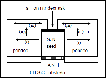
A schematic of the pendeo-epitaxial growth of GaN is illustrated in Figure 1. There are three primary stages associated with the pendeo-epitaxial formation of this material: (i) initiation of lateral homoepitaxy from the sidewalls of the GaN seed, (ii) vertical growth and (iii) lateral growth over the silicon nitride mask covering the seed structure. Pendeo-epitaxial growth of GaN was achieved within the temperature range of 1050-1100°C using the same pressure and V/III ratio used for the deposition of the GaN seed layer, as described above. Additional experimental details regarding the pendeoepitaxial growth of GaN and AlxGa1−xN layers employing 6H-SiC substrates are given in Refs. [Reference Zheleva, Smith, Thomson, Linthicum, Gerhke, Rajagopal and Davis14–Reference Zheleva, Thomson, Smith, Rajagopal, Linthicum, Gehrke and Davis19, Reference Gehrke, Linthicum, Rajagopal, Preble, Carlson, Robin and Davis22]. The morphology and defect microstructures were investigated using scanning electron microscopy (SEM) (JEOL 6400 FE) and transmission electron microscopy (TEM) (TOPCON 0002B, 200 KV). Determination of the degree of tilting in the PE GaN was achieved using X-ray diffraction (XRD) (Philips X’Pert MRD X-ray diffractometer) analysis. Optical characterization was performed via photoluminescence (PL) using a He-Cd laser (λ=325 nm).
Schematic of pendeoepitaxial growth from GaN sidewalls and over a silicon nitride mask.

Cross-sectional SEM of a GaN pendeo-epitaxial growth structure with limited vertical growth from the seed sidewalls and no growth on the seed mask.

Results and Discussion
Growth on SiC substrates
The pendeo-epitaxial phenomenon is made possible by taking advantage of growth mechanisms identified by Zheleva et al. [Reference Zheleva, Nam, Bremser and Davis8] in the conventional LEO technique and by using two additional key steps, namely, the initiation of growth from a GaN face other than the (0001) and the use of the substrate (in this case SiC) as a pseudo-mask. By capping the seed-forms with a growth mask, the GaN was forced to grow initially and selectively only on the GaN sidewalls. Common to conventional LEO, no growth occurred on the silicon nitride mask covering the seed forms. Deposition also did not occur on the exposed SiC surface areas at the higher growth temperatures employed to enhance lateral growth (the pseudo-mask effect). The Ga- and N-containing species more likely either diffused along the surface or evaporated (rather than having sufficient time to form GaN nuclei) from both the silicon nitride mask and the silicon carbide substrate. The pronounced effect of this is shown in Figure 3 wherein the newly deposited GaN has grown truly suspended (pendeo) from the sidewalls of the GaN seed structure. During the second PE event (ii), vertical growth of GaN occurred from the advancing (0001) face of the laterally growing GaN. Once the vertical growth became extended to a height greater than the silicon nitride mask, the third PE event (iii) occurred, namely, conventional LEOtype growth and eventual coalescence over the seed structure, as shown in Figure 3.
Cross-sectional SEM of a GaN/Al10 Ga90 N pendeo epitaxial growth structure showing coalescence over the seed mask.

A cross-sectional TEM micrograph showing a typical pendeo-epitaxial growth structure is shown in Figure 4. Threading dislocations extending into the GaN seed structure, originating from the GaN/AlN and AlN/SiC interfaces are clearly visible. The silicon nitride mask acted as a barrier to the further vertical propagation of these defects into the laterally overgrown pendeo-epitaxial film. Since the newly deposited GaN is suspended above the SiC substrate, there are no vertically oriented defects associated with the mismatches in lattice parameters between GaN and AlN and between AlN and SiC. Preliminary analyses of the GaN seed/GaN PE and the AlN/GaN PE interfaces revealed evidence of the lateral propagation of the defects; however, there is yet no evidence that the defects reach the (0001) surface where device layers will be grown. As in the case of LEO, there is a significant reduction in the defect density in the regrown areas.
Cross-sectional TEM of a GaN pendeo-epitaxial structure showing confinement of threading dislocations under the seed mask, and a reduction of defects in the regrowth.

The continuation of the pendeo-epitaxial growth results in coalescence with adjacent growth fronts and the formation of a continuous layer of GaN, as observed in Figure 5. This also results in the practical elimination of all dislocations stemming from the heteroepitaxial growth of GaN/AlN on SiC. Clearly visible in Fig. 5(a) are the voids that form when adjacent growth fronts coalesce. Optimization of the pendeo-epitaxial growth technique should eliminate these undesirable defects.
Micrographs taken via (a) cross-sectional SEM and (b) plan-view SEM of examples of pendeo-epitaxial growth with coalescence over and between the seed forms resulting in a single GaN layer.

Pendeo-epitaxial growth of individual forms and coalesced single layers of PE Al10Ga90N alloys and PE GaN as well as forms containing heterostructures of alternating layers of GaN and Al10Ga90N have been realized in this research as shown in Figure 3. Ref. [Reference Gehrke, Linthicum, Rajagopal, Preble, Carlson, Robin and Davis22] is discussing in more detail the process necessary to fabricate coalesced single layers of PE Al10Ga90N alloys and their characterization.
Growth on Silicon Substrates
Research regarding the development of process routes leading to the growth of III-Nitride films on Si has been less relative to the number of studies concerned with growth on sapphire and SiC. This has been due in part to the three-dimensional nucleation and growth of GaN islands caused by the combination of significant mismatches in lattice parameters, the higher surface energy of GaN and the chemical reactivity of Si with the reactants in the growth environment. To address the above concerns we have developed a process route similar to those used for growth of GaN on 6H-SiC(0001), but replaced the 6H-SiC substrate with a 3C-SiC(111) transition layer grown on a Si(111) substrate. The atomic arrangement of the (111) plane of 3C-SiC is equivalent to the (0001) plane of 6HSiC; this facilitates the sequential deposition of a high temperature 2H-AlN(0001) buffer layer of sufficient quality for the GaN seed layer, as discussed in Reference [Reference Weeks, Bremser, Ailey, Carlson, Perry and Davis20]. The 3CSiC layer is also exposed between the GaN seed forms and the seed forms are capped with a silicon nitride growth mask to force the GaN to grow initially and selectively only on the GaN sidewalls in the manner described above for growth using the 6H-SiC(0001) substrates.
For the initial demonstrations of PE growth of GaN films on silicon, 0.5 and 2 μm thick 3C-SiC(111) layers were deposited on 50 mm diameter, 250 µm thick converted Si(111) substrates. All subsequent research described below used the ∼2.0 µm barrier layer.
Figure 6 shows a cross-sectional SEM micrograph of a PE GaN layer grown laterally and vertically from raised GaN stripes etched in a GaN/AlN/3C-SiC/Si(111) substrate and over the silicon nitride mask atop each stripe.
Cross-sectional SEM micrograph of a coalesced PE GaN epilayer deposited on a 3C-SiC/Si(111) substrate.

Tilting between adjacent growth fronts over the mask regions are commonly observed in coalesced GaN epilayers grown using the LEO technique. This phenomenon was also determined to be present in the PE GaN films.
The FWHMs of the XRD rocking curves for the (0002) reflection are indicative of the crystallographic tilt and are dependent on the crystal orientation, as shown in Figure 7. The XRD spectrum taken along the [ 11
DCXRD analysis of the tilting in the coalesced PE films.

Unlike LEO, coalesced PE GaN epilayers contain two sets of coalesced growth fronts, namely, over the trenches and over the masks. A more sensitive method of evaluating the tilt in PE grown GaN is required to determine if it is present at both areas of coalescence. Selected area diffraction patterns were obtained using TEM and taken from a small area of coalescence in a trench region and near the region of coalescence over the silicon nitride mask. Analyses of these two patterns revealed no evidence of tilt in the laterally grown material over the trenches; however, significant tilt has occurred over the mask regions of the seed structures. Thus the mask has markedly influenced the crystallographic tilt in the overgrown film.
A typical room temperature PL spectrum for a PE GaN film grown on 2 μm wide raised stripes, oriented in the [ 1
Room temperature photoluminescence of a coalesced layer of PE GaN grown on an GaN/AlN/3CSiC/Si(111) substrate.

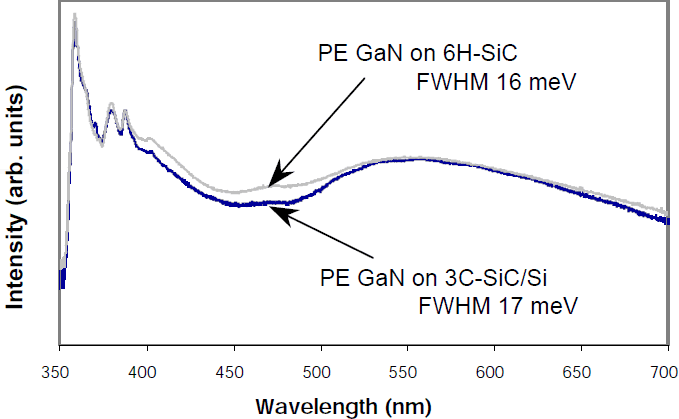
The low temperature (14K) PL spectrum on a logarithmic intensity scale showed a strong near band-edge emission at 359 nm (3.45 eV), as shown in Figure 9. The FWHM was 17 meV. Also included in Figure 9 is a low temperature PL spectrum of PE GaN grown on a GaN/AlN/6H-SiC substrate. The band-edge peak in the latter spectrum is at 358 nm (3.46 eV) with a FWHM of 16 meV.
Comparison of low-temperature (14K) PL spectra of PE GaN grown on GaN/Al/6H-SiC and GaN/AlN/3C-SiC/Si(111) substrates.

A comparison of these two spectra indicates that the optical character of the PE GaN grown on the 3C-SiC/Si substrate is nearly identical to the quality of the PE GaN grown on the 6H-SiC substrates. The band-edge of the PE GaN grown on Si is shifted by 10 meV to a slightly lower energy than that of the PE GaN grown on SiC, which is indicative of a slightly higher stress in the film of the former. As a further comparison, GaN(0001) films conventionally grown on AlN/6H-SiC substrates typically have a bandedge peak at 357.7 nm (3.466eV) and a FWHM of 4 meV.
Summary
Pendeo-epitaxy has been developed as an alternative and more simple approach of growing uniformly thin films with low densities of threading dislocations over the entire surface of a substrate. In particular, the growth of both discrete structures and coalesced GaN and AlxGa1−xN films and multilayer heterostructures using pendeo-epitaxy on etched GaN seed layers previously grown on AlN(0001)/6H-SiC(0001) and AlN(0001)/SiC(111)/Si(111) substrates has been demonstrated. Tilting in the coalesced GaN epilayers of 0.2° was confined to areas of mask overgrowth; no tilting was observed in the material suspended above the trenches. The strong, low-temperature PL band-edge peak at 3.45 eV with a FWHM of 17 meV was comparable to that observed in PE GaN films grown on 6H-SiC(0001). The band-edge in the material on Si(111) was shifted by 10 meV to a lower energy, indicative of a greater tensile stress.
Acknowledgements
The authors acknowledge Cree Research, Inc. and Motorola for the SiC and the silicon wafers respectively. This work was supported by the Office of Naval Research under contracts N00014-98-1-0384 (Colin Wood, monitor) and N00014-98-1-0654 (John Zolper, monitor). The authors also acknowledge CWRU and the Georgia Technology Research Institute for use of their clean room facilities.