


Piezotronic effect and piezotronics
The piezoelectric nanogenerator was first proposed in 2006 using ZnO nanowires.Reference Wang and Song1 The presence of a piezoelectric potential arising from piezoelectric polarization charges was proposed for understanding the observed electricity output by mechanical straining.Reference Gao and Wang2 At the same time, the piezoelectric-modulated potential barrier at the metal–ZnO interface was proposed to act as a “gate” voltage for explaining the observed transistor-like behavior of a metal–ZnO–metal structureReference Wang, Zhou, Song, Liu, Xu and Wang3 and the strain-gated diode effect at a metal–ZnO interface.Reference He, Hsin, Liu, Chen and Wang4 Following these early efforts, piezotronics was coined as the name for this new field in 2007.Reference Wang5–Reference Wang7
Fundamental effect
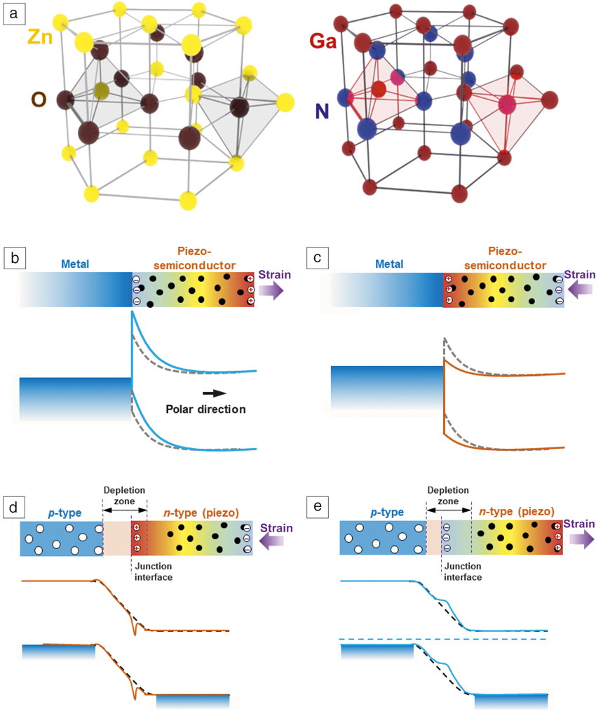
As for a metal–semiconductor interface, if the semiconductor has a noncentrosymmetric structure (Figure 1a) and the doping in the semiconductor is moderate, the static polarization charges at the interface arising from piezoelectric effects are not completely screened. The height of the Schottky barrier can then be modulated by the applied strain (tensile or compressive), resulting in tuning of the barrier electronic-transport properties by the piezoelectric effect. The lowered barrier can enhance electron transport, while an increased barrier height can cut off the current, just like a diode. This is the piezotronic effect, which involves using piezoelectric polarization charges as a “gating” voltage for tuning the electronic transport across an interface or junction (Figure 1b–e).Reference Zhou, Fei, Gu, Mai, Gao, Yang, Bao and Wang8,Reference Gao, Zhou, Gu, Fei, Hao, Bao and Wang9 The effect was further verified experimentally by the development of piezotronic strain-gated transistor and logic gates;Reference Wu, Wei and Wang10,Reference Liu, Lee, Ding, Liu and Wang11 the associated semiclassical theory was proposed recently.Reference Zhang, Liu and Wang12
The piezotronic effect. (a) The wurtzite crystal structures of ZnO and GaN. (b, c) Schematic energy diagrams illustrating the piezotronic effect in a Schottky contact when (b) tensile and (c) compressive strains are applied. The dashed and solid curves represent the band edges before and after the application of strain, respectively. (d, e) Schematic energy diagrams illustrating the piezotronic effect in a p–n junction when (d) tensile and (e) compressive strains are applied.Reference Wang7
Basic device structure and applications
Since the invention of piezotronics in 2007,Reference Wang5 rapid advances have been made in revealing the fundamental piezotronic process and implementing new device technologies. The basic structure of a typical piezotronic device includes two back-to-back Schottky contacts and a semiconducting channel, or two ohmic contacts and a p–n junction. The strain-induced polarization in the piezoelectric semiconductor (e.g., ZnO nanowires) can act as the controlling signal in the piezotronic devices.Reference Zhou, Fei, Gu, Mai, Gao, Yang, Bao and Wang8,Reference Zhou, Gu, Fei, Mai, Gao, Yang, Bao and Wang13 The asymmetric change in the strain-dependent current–voltage (I–V) curves for piezotronic transistors is characteristic of the piezotronic effect.
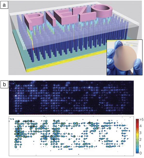
Piezotronic logic devices have been developed by integrating strain-gated piezotronic transistors for performing electronic logic computations over the mechanical strain signals.Reference Wu, Wei and Wang10 A piezotronically gated resistive memory device has also been demonstrated for recording strain information.Reference Wu and Wang14 The feasibility of p-type piezotronic devices has been explored to develop a comprehensive understanding of the piezotronic effect.Reference Pradel, Wu, Zhou, Wen, Ding and Wang15 The piezotronic principle also enables new possibilities for the design and implementation of three-dimensional nanoelectronics, such as incorporating high-density array integration of vertical nanowire transistors (Figure 2),Reference Wu, Wen and Wang16 where these independently addressable two-terminal piezotronic transistors can convert mechanical stimuli into local electronic controlling signals.Reference Wu, Wen and Wang16
Three-dimensional piezotronic transistor array for tactile imaging.Reference Wu, Wen and Wang16 (a) Two-terminal strain-gated vertical piezotronic transistor. c represents [0001] of the ZnO nanowire. (b) (i) The structure of the piezotronic transistor array. Inset: Scanning electron microscope image of the ZnO nanowires in a pixel of a vertical piezotronic transistor. (ii) Three-dimensional perspective view of the topological profile image for the array device (in the area highlighted by the white dashed box) with the color gradient representing different heights. (c) The optical image of such array devices on a 4-in. (10 cm) poly(ethylene terephthalate) substrate. Reproduced with permission from Reference Reference Wu, Wen and Wang16. © 2013 AAAS. Note: NW, nanowire; SU 8, commonly used epoxy-based negative photoresist.

Schottky-contact-based piezotronic devices have been demonstrated using a wide range of one-dimensional piezoelectric semiconductors (e.g., GaN, CdS, InAs, and InN) in addition to ZnO. The p–n junction-based piezotronic devices mainly rely on the heterojunction structures formed between n-type and p-type inorganic or organic semiconductors. Because many nanostructured piezoelectric semiconductors spontaneously grow along their polar directions, the distribution of the piezoelectric field is along the semiconducting channel upon straining, and the piezotronic effect only modulates the electronic transport at the reverse-biased Schottky contact or the p–n junction (Figure 1b–e). Some piezoelectric semiconductors can also grow along nonpolar directions (e.g., m-plane GaN nanowires, a-axis GaN nanobelts, and a-axis ZnO nanobelts) and the strain-induced piezoelectric field is distributed along the direction perpendicular to the channel and directly modulates channel transport.
The piezotronic effect has also been utilized to develop Schottky-contact-based sensors with significantly enhanced performance (e.g., biochemical sensors, gas sensors, and humidity sensors), where the sensitivity enhancement is due to Schottky barrier height modulation by strain-induced polarization charges.Reference Zhou, Hu, Yu, Pan and Wang17,Reference Niu, Hu, Wen, Zhou, Zhang, Lin, Wang and Wang18 The Hu et al. articleReference Hu, Kalantar-Zadeh, Gupta and Liu19 in this issue reviews the fundamental principles of piezotronics and technological advances in the integration of large-scale piezotronic array devices for sensors and electronics. In their article in this issue, Frömling et al. discuss advances in utilizing piezotronic devices for various sensor applications.Reference Frömling, Yu, Mintken, Adelung and Rödel20
Piezo-phototronic effect and piezo-phototronics
The piezo-phototronic effect was discovered in 2010 when the coupling of piezoelectricity, photoexcitation, and semiconductor transport in a metal–ZnO system was being explored. It was found that while the piezoelectric effect can effectively increase the Schottky barrier height, photon excitation lowers the Schottky barrier due to increased local carrier density, resulting in tuning of optoelectronic processes.Reference Hu, Chang, Fei, Snyder and Wang21,Reference Hu, Zhang, Chang, Snyder and Wang22 The piezo-phototronic effect allows for tuning of piezoelectric polarization charges present at a p–n junction, affecting carrier separation, recombination, or transport process. The piezo-phototronic effect was first applied to tune the performance of light-emitting diodes (LEDs),Reference Yang, Wang, Xu and Wang23 solar cells,Reference Yang, Guo, Zhang, Ding, Wang and Wang24,Reference Pan, Niu, Ding, Dong, Yu, Liu, Zhu and Wang25 and photosensors,Reference Yang, Guo, Wang, Zhang, Xu, Lien and Wang26 and the corresponding theory was proposed in 2012.Reference Zhang, Yang and Wang27–Reference Zhang and Wang29 The article by Zhang et al.Reference Zhang, Leng, Willatzen and Huang30 in this issue reviews recent progress in the theoretical study of the fundamental piezotronic and piezo-phototronic effects, and provides perspectives for materials considerations and design guidance for future device implementation.
The three-way coupling among piezoelectricity, semiconductor transport, and light–matter interaction in piezoelectric semiconductors enables the design and implementation of a new class of active and adaptive optical devices, piezo-phototronics, in which the behaviors of photoexcited carriers can be directly engineered by mechanical stimulation.Reference Yang, Wang, Xu and Wang23,Reference Zhang, Yang and Wang27,Reference Liu, Yang, Zhang, Yang and Wang28 After the 2010 reports demonstrating the first piezo-phototronic devices using ZnO nanowires,Reference Wang and Song1,Reference Hu, Chang, Fei, Snyder and Wang21 intensive efforts have been devoted to explore the fundamental piezo-phototronic process in devices (e.g., strain-gated flexible nano-LEDs, photodetectors, and solar cells). The Bao et al. articleReference Bao, Hu, Yang and Pan31 in this issue describes the fundamental principles of piezo-phototronics and summarizes recent advances in designing and implementing piezo-phototronically tuned adaptive optoelectronic devices.
In a piezo-phototronic photodetector, the separation and extraction of photogenerated carriers at a p–n junction or a Schottky barrier, and thereby, the photodetection figures of merit such as photoresponsivity and response time can be significantly enhanced by the piezo-phototronic engineering of the interfacial energetics. The performance of a piezo-phototronic LED (e.g., the emission intensity) can be effectively modulated and enhanced through the engineering of the injection, transport, and recombination of electron–hole pairs via the piezo-phototronic effect. Piezo-phototronic engineering also enables the development of LED array devices consisting of patterned vertical p–n heterojunctions for mapping spatial pressure distributionsReference Bao, Wang, Dong, Yu, Zhao, Wang and Pan32,Reference Pan, Dong, Zhu, Niu, Yu, Yang, Liu and Wang33 (Figure 3). The emission intensity of the LED sensors is dictated by locally applied strains that control the transport and recombination of electrons and holes in the LED device. Therefore, spatial pressure distributions can be obtained by parallel-reading the illumination intensities of the array device (Figure 3b).
Piezo-phototronic light-emitting diode (LED) array for pressure imaging.Reference Zhang and Wang29 (a) Structure of the piezo-phototronic LED array fabricated on a GaN wafer. (Inset) Optical image of the piezo-phototronic LED array on a 5-cm GaN wafer. (b) (Upper) Electroluminescence image of the array device for (lower) pressure imaging. The color bar represents the enhancement factor of the piezo-phototronic LED intensity under strain compared to that without strain. Reproduced with permission from Reference Reference Zhang and Wang29. © 2012 Nature Publishing Group.
The piezo-phototronic principle can also be used to engineer the photoelectrochemical process at the semiconductor–electrolyte interface for efficient photoanodes, improved photocatalysts, and enhanced redox reactions.Reference Wang, Liu, Wang, Zhou, Qin and Wang34–Reference Zhao, Zhang, Wang, Hu, Wang, Ma, Liu, Wang and Sang36 The Wang et al. article in this issue discusses the fundamental principle of piezo-catalysis and the application of piezotronic effects in designing more efficient catalysts.Reference Wang, Rohrer and Li37 The piezo-phototronic effect can also exist in p-type third-generation semiconductors (e.g., p-type GaN)Reference Hu, Zhang, Lin, Ding, Zhu and Wang38,Reference Yu, Dong, Pan, Niu, Liu, Liu, Chua, Chi and Wang39 and can be used for implementing optomechanical logic devices.Reference Yu, Wu, Pan, Wang, Ding and Wang40
Piezophotonic effect
The piezophotonic effect was first predicted in 2008, which indicated that photons can be emitted as driven by a strong local piezoelectric field.Reference Wang41 Later, this effect was first experimentally observed by Hao’s group using a two-step process,Reference Wong, Chen, Tsang, Zhang and Hao42 in which a mechanical straining stage was used to periodically strain a luminescent material, resulting in photon emission. Subsequently, the piezophotonic effect was demonstrated for the ZnS:Mn system as a result of piezoelectric field-induced band tiltingReference Wang, Zhang, Yu, Dong, Peng, Zhang, Zhang, Liu, Pan and Wang43 and the release of surface state trapped electrons, followed by their transition to lower energy hole states. The released energy excites trapped quasi-free electrons in the doping states that transit back to the vacant impurity states of Mn, resulting in photon emission. The strain-induced polarization charges can be used to modulate the luminescent processes from phosphors through piezo-photonic coupling, which initiates and controls the mechanoluminescence process during the conversion from mechanical stress to light emission. In their article, Hao and Xu discuss the principles of piezophotonics and describe recent advances in developing piezophotonic devices.Reference Hao and Xu44
In a typical piezophotonic device, light emission from the phosphor is induced by the polarization charges from the piezoelectric material, which provides a new type of coupling between piezoelectric and photonic characteristics. Flexible piezophotonic luminescence devices built using composite phosphors have also been demonstrated, in which the luminescence intensity strongly depends on the applied strain rate.Reference Chen, Wong, Bai, Jie and Hao45 Piezophotonic engineering of the mechanoluminescence process, where mechanical action on a solid causes light emission, also enables the design and implementation of flexible sensor array devices for dynamic pressure mapping.Reference Wang, Zhang, Yu, Dong, Peng, Zhang, Zhang, Liu, Pan and Wang43 The luminescence wavelength can also be modulated by the piezophotonic coupling,Reference Wong, Chen, Tsang, Zhang and Hao42 offering new possibilities in a wide range of sensor and imaging applications.
Impact on third-generation semiconductors
Third-generation semiconductor materials, represented by wide bandgap GaN and SiC, have attracted intensive interest for emerging technologies in consumer electronics, 5G communication systems, electric vehicles, optoelectronics, and defense applications, due to their superior material characteristics, including high-voltage resistance, high-switching frequency, high-temperature resistance, and high-radiation resistance.Reference Millán, Godignon, Perpiñà, Pérez-Tomás and Rebollo46 The wide bandgap nature and strong piezoelectric characteristics of these materials suggest that piezotronic and piezo-phototronic couplings can be significant, providing ideal platforms for exploring the fundamental coupling between the piezoelectricity and a plethora of intriguing processes, such as high-frequency transport, high-field operation, and two-dimensional (2D) electron gas in related device structures.Reference Wang, Yu, Jiang, Hu, Wu, Ding, Peng, Li and Wang47
Knowledge gained through carrying out these fundamental explorations is expected to positively impact the design and development of related devices with enhanced performance and efficiency (e.g., high-electron-mobility transistorsReference Jiang, Liu, Du, Huang, Liu, Zhao, Li, Pu, Zhai and Hu48 and insulated-gate bipolar transistors), critical for societally pervasive technologies.Reference Du, Hu and Wang49,Reference Wang, Peng, Pan and Wang50 In addition to associated fundamental interests and technological potential, it is expected that research and development efforts on piezotronic, piezo-phototronic, and piezophotonic effects on third-generation semiconductors will also be advanced and boosted by the commercial feasibility and maturity of related technological processes in manufacturing and integrating these materials.Reference Millán, Godignon, Perpiñà, Pérez-Tomás and Rebollo46
Impact on 2D materials
One-dimensional nanomaterials and thin-film structures have been the primary focus for elucidating and utilizing piezotronic and piezo-phototronic effects. Recent studies show that 2D materials (e.g., monolayer transition-metal dichalcogenides [TMDCs]), exhibit strong piezoelectricity due to their noncentrosymmetric structures. Together with their high crystallinity and excellent semiconducting and superior mechanical properties, this suggests the promise of 2D TMDCs as high-performance piezotronic materials, especially inspired by the first report on piezotronic coupling in atomically thin MoS2.Reference Wu, Wang, Li, Zhang, Lin, Niu, Chenet, Zhang, Hao, Heinz, Hone and Wang51
Significant advances have also been achieved in studying piezoelectricity and the piezotronic effect in various 2D materials.Reference Qi, Lan, Stieg, Chen, Zhong, Li, Chen, Zhang and Wang52–Reference Liu, Yang, Gao, Yang, Liu, Li, Lou, Shen, Liao, Pan and Wang61 The study of piezoelectricity and piezotronic effects in 2D materials is an emerging field. In their article in this issue, Liu et al. summarize the progress made in related fields.Reference Liu, Wahyudin, He and Zhai62 These early works suggest the feasibility and great potential of studying the fundamental piezotronic effect and its coupling with intriguing physical processes such as quantum transport and topological properties in materials systems with much reduced and controlled dimensionality. These fundamental explorations could enable applications in powering nanodevices, stretchable electronics, and optoelectronics with components only a few atomic layers thick. Meanwhile, the realization of the full potential for 2D materials in piezotronics and piezo-phototronics demands advances in producing high-quality 2D materials both scalably and reliably.
Future perspectives
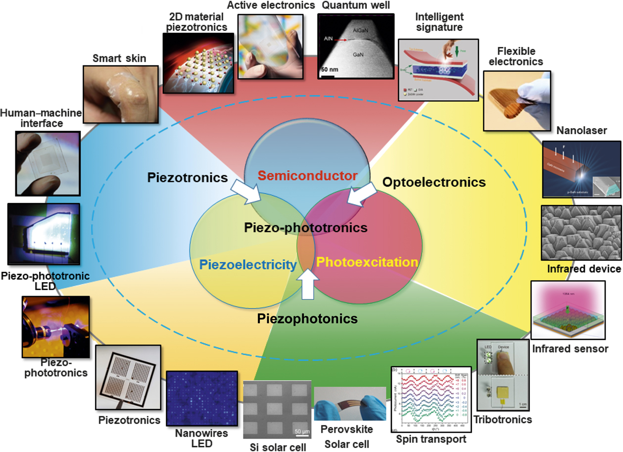
Piezotronics and piezo-phototronics are two fields characterized by actively coupling the strain-induced polarization potential with the mobile charge-carrier transport behavior in third-generation semiconductors. They are likely to impact the design and fabrication of electronic and photonic devices for mechanosensation, human–machine interfacing, robotics, artificial intelligence, sensors, LEDs, solar cells, and catalysis (Figure 4). Further advancements of these fields require fundamental understanding of physics, quantum mechanical calculations, and technological implementations of piezotronic and piezo-phototronic devices.Reference Zhu, Zhang, Lin, Wang, Yang, Chen, Wang, Chen and Wang63,Reference Hu, Zhang, Li and Wang64 Sophisticated characterization methods such as direct probing of the interfacial dynamics and determination of the distribution of piezoelectric polarization charges are required to provide reliable interpretation of the fundamental materials and structural characteristics related to the piezotronic and piezo-phototronic effects. Optimization and exploration of materials, as well as design, fabrication, and characterization of arrays of piezotronic devices are essential to promote applications, ranging from a single device to a practically workable system. We anticipate that the integration of piezotronic and piezo-phototronic effects and devices with current electronics, optoelectronics, and quantum devices will bring revolutionary impacts to sensor, artificial intelligence, energy, and human-integrated technologies.
The plethora of opportunities for fundamental research and technological implementation in piezotronics and piezo-phototronics. The three-way active coupling among piezoelectricity, photoexcitation, and semiconducting properties in piezoelectric semiconductor materials is the fundamental process for piezotronics, piezophotonics, and piezo-phototronics. This diagram shows the potential applications that have been demonstrated using the piezotronic and piezo-phototronic effects in various fields. Note: LED, light-emitting diode.
Acknowledgments
We would like to thank the following colleagues who made significant contributions to the field of piezotronics and piezo-phototronics: J. Zhou, J.-H. He, Y. Hu, Y. Zhang, Q. Yang, C. Pan, X. Wen, R. Yu, Y. Liu, W. Hu, J. Zhai, X. Wang, L.P. Zhu, and many others.

Zhong Lin Wang is the Hightower Chair in Materials Science and Engineering and Regents’ Professor at the Georgia Institute of Technology, as well as Founding Director and Chief Scientist of the Beijing Institute of Nanoenergy and Nanosystems, Chinese Academy of Sciences, China. He received his PhD degree in physics from Arizona State University in 1987 and his BS degree in applied physics from Xidian University, Xian, China, in 1982. His research interests include self-powered nanosystems and energy for micro-nanosystems. Wang coined and pioneered the field of piezotronics and piezo-phototronics. He has been cited more than 190,000 times and has an h-index of 216. He is ranked No. 1 in Google Scholar public profiles in Nanotechnology and Nanoscience both in total citations and h-index impacts. He received the ENI Award in Energy Frontiers in 2018. Wang can be reached by email at zhong.wang@mse.gatech.edu.

Wenzhuo Wu is the Ravi and Eleanor Talwar Rising Star Assistant Professor in the School of Industrial Engineering at Purdue University. He was a postdoctoral fellow in the School of Materials Science and Engineering at the Georgia Institute of Technology (Georgia Tech) from 2013 to 2015. He received his PhD degree from Georgia Tech in materials science and engineering in 2013. Wu’s research interests include the design, manufacturing, and integration of nanomaterials and devices for applications in electronics, sensors, and self-powered micro-/nanosystems. He was a recipient of the Oak Ridge Associated Universities Ralph E. Powe Junior Faculty Enhancement Award in 2016 and the IOP Semiconductor Science and Technology Best Early Career Research in 2017. Wu can be reached by email at wu966@purdue.edu.

Christian Falconi has been an assistant professor at the University of Rome Tor Vergata, Italy, since 2002, adjunct professor at the Sungkyunkwan University, Republic of Korea, since 2013, and adjunct professor at the Beijing Institute of Nanoenergy and Nanosystems, Chinese Academy of Sciences, China, since 2017. He received his MSc degree in 1998 and his PhD degree in 2001 in electronic engineering from the University of Rome Tor Vergata. His research interests include electronics, sensors, microsystems, nanosystems, nanogenerators, and piezotronics. Falconi can be reached by email at falconi@eln.uniroma2.it.


