


Introduction
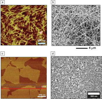
Transparent electrodes are a fundamental component in many modern devices such as liquid-crystal displays (LCDs), touch panels, e-paper, organic light-emitting diodes (OLEDs), and solar cells. The demand for all of these devices continues to grow, spurring demand for transparent electrodes. The market for transparent conductors is expected to reach $6.9 billion in revenues by 2016.1 Traditionally, the material of choice is a sputtered metal oxide, the most common of which is indium tin oxide (ITO). ITO was first synthesized and studied in the 1940s, and has been well developed over the last 50 years. ITO has retained its dominance due to its superior combination of high optical transparency and low resistance, the two most important features of a transparent conductor; emerging nanomaterials have struggled to compete with ITO in this respect. However, ITO is also prone to several major problems. The supply of indium is constrained by both mining and geo-political issues; therefore, indium is relatively expensive, having its price peaking at over $800/kg in 2006, and this cost is reflected in ITO pricing. Adding to the cost of ITO is the expense of setting up and maintaining a sputter deposition line, as well as the low deposition yields. In addition to cost, ITO suffers from being quite brittle, showing cracks at relatively low strains, which lead to a sharp increase in resistance. This is already a problem in many of today’s devices, and promises to be an even bigger issue in future flexible electronics. Fortunately, recent advances in nanomaterials synthesis, purification, and solubilization have led to the emergence of viable alternatives to ITO.Reference Hecht, Hu and Irvin2 The materials most often considered to replace sputtered ITO include nanostructured ITO,Reference Wan, Dattoli, Fung, Guo, Chen, Pan and Lu3–Reference Mahajeri, Voigt, Taylor, Reindl and Peukert5 conducting polymers,Reference Kirchmeyer and Reuter6–Reference Ha, Nikolov, Pollack, Mastrangelo, Martin and Shashidhar8 nanostructured silver,Reference De, Higgins, Lyons, Doherty, Nirmalraj, Blau, Boland and Coleman9–Reference Hu, Kim, Lee, Peumans and Cui12 carbon nanotubes (CNTs),Reference Hu, Hecht and Gruner13–Reference Wu, Chen, Du, Logan, Sippel, Nikolou, Kamaras, Reynolds, Tanner, Hebard and Rinzler15 and graphene.Reference Wassei and Kaner16, Reference Cai, Zhu, Li, Piner and Ruoff17 Figure 1 shows micrographs of thin films, or networks, of these nanoscale materials. The nanoscale dimensions of these conductors enable them to be solubilized into “inks,” which can then be used to print electrodes using existing solution-based printing processes. Printing has several advantages, such as enabling lower capital equipment cost, higher throughputs, and additive patterning. This issue of MRS Bulletin focuses on these printable material alternatives to traditional sputtered metal oxides for use as transparent electrodes.
Atomic force microscopy/scanning electron microscopy images of transparent conducting films of (a) carbon nanotubes. Reprinted with permission from Reference Reference Li, Hu, Wang, Zhou, Gruner and Marks48. ©2010, American Chemical Society. (b) Silver nanowires. Reprinted with permission from Reference Reference Hu, Kim, Lee, Peumans and Cui12. ©2010, American Chemical Society. (c) Graphene flakes. Reprinted with permission from Reference Reference Li, Muller, Gilje, Kaner and Wallace36. ©2008, Nature Publishing Group. (d) Indium tin oxide nanoparticles. Reprinted with permission from Reference Reference Mahajeri, Voigt, Taylor, Reindl and Peukert5. ©2010, Elsevier.
Optoelectronic properties
The two most important features for a transparent conducting material are its sheet resistance (R s) and optical transparency (VLT), with different applications having different requirements. Typically, a R s lower than 1000 Ω/sq and a VLT greater than 85% are required. Grüner et al. developed a suitable metric to compare the performance of various transparent conductors; Coleman et al.Reference Hu, Hecht and Gruner14, Reference De and Coleman18 further studied this metric. This metric uses the measured film R s and VLT to compute a single parameter, the ratio of the dc conductivity (σdc) to optical conductivity (σop), with higher values translating to better performance for use as a transparent conductor (see Equation 1).
In Equation 1, μ0 ∼ 1.26 × 10⁻⁶ H·m–1 is the vacuum permeability, and ε0 ∼ 8.85 × 10⁻¹² F·m–1 is the vacuum permittivity. The ratio σdc/σop serves as a figure of merit (FOM) and allows comparison between films of various thicknesses and various materials (i.e., carbon nanotubes [CNTs] to graphene to poly(3,4-ethylenedioxythiophene) [PEDOT]). Currently, metallic nanomaterials such as silver nanowires have the highest σdc/σop ratios, up to 415,Reference De, Higgins, Lyons, Doherty, Nirmalraj, Blau, Boland and Coleman9 making them the only nanomaterial alternative to compete with and often surpass ITO in terms of R s and VLT. To date, the best graphene films have a σdc/σop ratio of 116 (30 Ω/sq and 90% VLT).Reference Bae, Kim, Lee, Xu, Park, Zheng, Balakrishnan, Lei, Kim, Song, Kim, Kim, Ozyilmaz, Ahn, Hong and Iijima19 This value is for graphene films made via chemical vapor deposition (CVD). For graphene films made via solution methods, this ratio varies over many orders of magnitude, with the best on the order of 1–10.Reference Wu, Agrawal, Becerril, Bao, Liu, Chen and Peumans20, Reference Biswas and Drzal21 This is compared to solution-processed CNT films with a highest reported σdc/σop ratio of 64.1 (60 Ω/sq and 90.1% VLT).Reference Hecht, Heintz, Lee, Hu, Moore, Cucksey and Risser22 Typically, the FOM can be increased by increasing the dc conductivity of the material, which is affected by many factors, such as material purity, geometry, density, and doping level. Careful optimization of this FOM is one of the remaining challenges for ITO alternatives. The article by De and Coleman in this issue discusses the FOM in more detail, with a focus on how the physics of percolation can affect the FOM for thin films typically used in transparent conductive coatings.
It is surprising that films based on CNTs can be made transparent, given that vertical forests of CNTs have been shown to be one of the blackest materials that exists (i.e., it is an ideal light absorber).Reference Yang, Ci, Bur, Lin and Ajayan23 Due to the nanoscale nature of these materials, ultra-thin layers can be printed with an average thickness less than 10 nanometers, thus allowing transmission of light even through a highly absorbing material. As an alternative to printing a thin layer of material, an opaque conductive material such as silver nanoparticles can be printed in a grid pattern. Although no light actually passes through the material at the location of the nanoparticles, 100% of light can pass through the gaps in the grid where no material is present. Thus, the grid, on average, will transmit some percentage of light, depending on the grid line width and pitch, and yet will maintain uniform conduction across lengths much greater than the line pitch. More information regarding printed conductive grids is included in the article by Woerle and Rost.
Inks and coatings
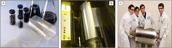
One of the most attractive properties of using these nanoscale materials as transparent conductive films is their ability to be dissolved into an ink and printed roll-to-roll (see Figure 2). Printing can be performed at high speeds up to 100 m/minute on flexible or rigid substrates several meters wide. Printing is less wasteful than sputtering, with nearly all the material being applied to the substrate, and can enable additive patterning. The printing process leverages such well-developed printing methods as slot-die, gravure, reverse roll, Mayer rod, aerosol jet, and screen printing. Inkjet printing of an ITO nanowire solution is discussed in detail by Dattoli and Lu in this issue. Making well-dispersed inks from nanoscale materials can be a challenge due to the large Van der Waals intermolecular forces that cause the nanoparticles to stick together. Typically, the use of one or more surfactants as well as high-powered agitation via sonication or high shear mixing is required to obtain a well-dispersed ink. Surfactant and mixing optimization to obtain inks where the nanomaterials are not agglomerated or bundled is one of the most critical steps in the process of making inks to print films with a high FOM. Ink formulation is critical to commercial success. Inks must be formulated to have a surface tension and viscosity appropriate for the coating method. If surfactants are used, bubbles or foam can cause difficulties in production, so the use of suitable anti-foamants may be necessary. For screen printable inks, high viscosity requirements will necessitate either very high solids loading or the addition of high molecular weight fillers. Additives to increase wetting, leveling, flow, adhesion, and elimination of bacteria are typical for many ink formulations. Care must be taken to choose additives that will not adversely affect the optoelectronic properties of the resulting conductive film or induce premature agglomeration of the dispersion. For printing of PEDOT films, the use of a high boiling point solvent additive serves as a “conductivity enhancer,” acting as a plasticizer that can modify the final film morphology. The article by Elschner and Lovenich discusses the use of conductivity enhancers as additives in more detail, in addition to other specifics of PEDOT formulation and coatings.
(a) Vials of carbon nanotube (CNT) inks; (b) a CNT conductive film being coated by a slot-die; and (c) a roll of printed transparent conducting film of CNT on poly(ethylene terephthalate).
Graphene
One nanomaterial being investigated as a printable transparent electrode is graphene, the two-dimensional allotrope of carbon. Graphene is one of the most broadly researched materials in recent years, and its many unique properties have been well documented in several reviews.Reference Allen, Tung and Kaner24–Reference Castro Neto, Guinea, Peres, Novoselov and Geim27 In fact, although it was only first experimentally isolated in 2004,Reference Novoselov, Geim, Morozov, Jiang, Zhang, Dubonos, Grigorieva and Firsov28 Konstantin Novoselov and Andre Geim (University of Manchester) have already earned the Nobel prize in physics (in 2010) for their work on graphene. Graphene was immediately recognized as a material with the potential to revolutionize many industries. It is the most nascent nanomaterial investigated as a transparent conducting electrode, especially via solution-based processing.
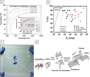
Graphene is a zero bandgap semiconductor possessing a room-temperature mobility on the order of 104 cm2/Vs with an electron/hole concentration up to 1013/cm2.Reference Novoselov, Geim, Morozov, Jiang, Zhang, Dubonos, Grigorieva and Firsov28 These electronic properties give graphene its exceptional in-plane conductivity, enabling it to have a rather low sheet resistance despite being a single atomic layer (0.34 nm) in thickness. Graphene absorbs 2.3% of incident visible light per layer (as shown in Figure 3a),Reference Nair, Blake, Grigorenko, Novoselov, Booth, Stauber, Peres and Geim29 and a single layer of graphene has almost no light lost due to reflection. Therefore, one can write the light transmission through a thin graphene stack as VLT(%) = 100% – 2.3%*N, where N is the number of graphene layers. Furthermore, the sheet resistance of a doped layer of graphene scales as 62.4 Ω/N.Reference Wu, Agrawal, Becerril, Bao, Liu, Chen and Peumans20 Together, these two facts combine for some startling theoretical properties, such as a predicted sheet resistance of 62.4 Ω/sq and 97.7% VLT for a single graphene sheet and 15.6 Ω/sq and 90.8% VLT for four sheets. If realizable, these values are more than suitable for most commercial applications. However, to date, experimental results have not equaled this theoretically limiting performance (Figure 3b), with solution-processed graphene typically the poorest performer among the materials covered in this issue. What is limiting the optoelectronic performance of graphene films from what is theoretically possible? Here, an analogy with CNTs may be useful. For CNTs, the largest source of resistance in a macroscopic film comes at the intersections between CNT bundles. Therefore, longer CNTs tend to lead to films with higher conductivities.Reference Hecht, Hu and Gruner30 Similarly, for graphene films consisting of a random network of overlapping graphene flakes, larger flakes are desirable to optimize performance. Also, for CNT films, it is thought that smaller CNT bundles lead to higher conductivity; this is because inner tubes within a bundle may be partially shielded from electrical contact with the overall network, and so will not fully participate in the current carrying capacity of the network.Reference Hecht, Hu and Gruner30 Similarly, graphene films consisting of fewer layers of graphene should be advantageous (with a true monolayer of graphene being optimal). Of course, maintaining the perfection of the graphene lattice is critical, as defects will introduce scattering sites that will increase resistance. Furthermore, surfactants or other dispersants used in the liquid phase will lower the overall film conductivity if not completely removed after film deposition. Doping will also play a critical role in enhancing the performance of graphene films. The sheet resistance of undoped graphene is on the order of 6000 Ω/sq,Reference Geim and Novoselov26 but this can be reduced via chemical doping by materials such as polyvinyl alcohol (n-type doping)Reference Blake, Brimicombe, Nair, Booth, Jiang, Schedin, Ponomarenko, Morozov, Gleeson, Hill, Geim and Novoselov31 or nitric acid (p-type doping).Reference Bae, Kim, Lee, Xu, Park, Zheng, Balakrishnan, Lei, Kim, Song, Kim, Kim, Ozyilmaz, Ahn, Hong and Iijima19 For real-world applications, it is important to test the stability of dopants under such accelerated aging conditions as high heat, humidity, and UV light.
(a) Transmittance versus wavelength for graphene films of one to four layers. Each layer of graphene absorbs about 2.5% of light at 550 nm. The inset shows little change in transmission after doping with nitric acid. (b) Visible light transmission (%) versus sheet resistance for graphene films made via various techniques (RGO, reduced graphene oxide; CMG, chemically modified graphene), compared to what is required by the industry and what is theoretically possible for perfect, highly doped graphene. Black square at 30 OPS and 90% T was added by the authors of this article to reflect the data of Bae et al. (Reprinted with permission from Reference Reference De and Coleman18. ©2010, American Chemical Society). (c) An image of large area graphene film on poly(ethylene terephthalate) grown roll-to-roll by chemical vapor deposition. Reprinted with permission from Reference Reference Bae, Kim, Lee, Xu, Park, Zheng, Balakrishnan, Lei, Kim, Song, Kim, Kim, Ozyilmaz, Ahn, Hong and Iijima19. ©2010, Nature Publishing Group. (d) A schematic showing solution processing of graphene/carbon nanotube hybrid film using hydrazine.
Graphene processing
The first reported synthesis of true monolayer graphene is attributed to Geim et al. in 2004,Reference Novoselov, Geim, Morozov, Jiang, Zhang, Dubonos, Grigorieva and Firsov28 and involved essentially a microscope, tape, and a pencil. Graphene platelets were mechanically cleaved from a piece of graphite by repeating peeling with Scotch tape, and single graphene layers were spotted using optical interference with the underlying substrate. This discovery marked the beginning of the rush toward graphene research. Subsequently, there have been many different methods to make graphene that have been explored and covered in several reviews.Reference Zhu, Murali, Cai, Li, Suk, Potts and Ruoff32, Reference Li and Kaner33 The best transparent electrode films based on graphene have been made by CVD growth on copper foils, followed by subsequent transfer of the graphene film to a polymer substrate and chemical doping, leading to a R s of 30 Ω/sq and 90% VLT (an image of such a film is shown in Figure 3c).Reference Bae, Kim, Lee, Xu, Park, Zheng, Balakrishnan, Lei, Kim, Song, Kim, Kim, Ozyilmaz, Ahn, Hong and Iijima19 Other common graphene production methods include epitaxial growth,Reference Berger, Song, Li, Wu, Brown, Naud, Mayou, Li, Hass, Marchenkov, Conrad, First and de Heer34 bottom-up organic synthesis,Reference Cai, Ruffieux, Jaafar, Bieri, Braun, Blankenburg, Muoth, Seitsonen, Saleh, Feng, Mullen and Fasel35 and chemical exfoliation of either graphite or graphite oxide (typically followed by reduction to graphene after deposition).Reference Li, Muller, Gilje, Kaner and Wallace36, Reference Stankovich, Dikin, Dommett, Kohlhaas, Zimney, Stach, Piner, Nguyen and Ruoff37 Chemical exfoliation is an intriguing approach from a manufacturing standpoint because it leads to solution phase processing of a graphene “ink,” which enables the use of high-speed printing of graphene films. Similar to the approach used for solution phase dispersions of CNTs, chemical exfoliation via solvents such as N-Methylpyrrolidone,Reference Hernandez, Nicolosi, Lotya, Blighe, Sun, De, McGovern, Holland, Byrne, Gun’ko, Boland, Niraj, Duesberg, Krishnamurthy, Goodhue, Hutchison, Scardaci, Ferrari and Coleman38, Reference Dubin, Gilje, Wang, Tung, Cha, Hall, Farrar, Varshneya, Yang and Kaner39 chloroform,Reference Biswas and Drzal21 or surfactant stabilized aqueous dispersionsReference Gruner, Hu and Hecht40, Reference Lotya, Hernandez, King, Smith, Nicolosi, Karlsson, Blighe, De, Wang, McGovern, Duesberg and Coleman41 are common approaches. Tung et al. have demonstrated a hybrid CNT/graphene solution using hydrazine as a solvent, thus providing a surfactant-free route toward high-performance films (Figure 3d).Reference Tung, Chen, Allen, Wassei, Nelson, Kaner and Yang42 Typically, exfoliation is aided by the use of ultrasonication followed by centrifugation to remove the thickest flakes. Ultimately, these solution-based dispersion processes need to continue to improve their ability to exfoliate and stabilize large area graphene sheets. Further improvements in graphene solubilization and deposition are needed to close the performance gap in FOM between solution processed and CVD grown graphene.
Applications: Beyond sheet resistance and transmission
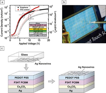
Alternative transparent conductors have already been demonstrated in devices such as LCDs,Reference Lai, Ou, Tsai, Chuang, Ma and Liang10, Reference Blake, Brimicombe, Nair, Booth, Jiang, Schedin, Ponomarenko, Morozov, Gleeson, Hill, Geim and Novoselov31 solar cells,Reference Wang, Zhi and Mullen43–Reference Gaynor, Lee and Peumans47 OLEDs,Reference Wu, Agrawal, Becerril, Bao, Liu, Chen and Peumans20, Reference Li, Hu, Wang, Zhou, Gruner and Marks48 and touch screens (see Figure 4).Reference Bae, Kim, Lee, Xu, Park, Zheng, Balakrishnan, Lei, Kim, Song, Kim, Kim, Ozyilmaz, Ahn, Hong and Iijima19, Reference Hecht, Thomas, Hu, Ladous, Lam, Park, Irvin and Drzaic49 Basic functionality has been verified, but to make real world, practical devices, many factors must be considered. Typically, an analysis of transparent conductors focuses on the sheet resistance and transparency of a coating, often ignoring other critical factors. Even the sheet resistance and transparency do not tell the entire optoelectronic story and can be misleading, as evidenced by several optoelectronic requirements for touch screen applications.
(a) An organic light-emitting diode with a solution processed graphene electrode shows similar performance to that with an indium tin oxide electrode in terms of current density (filled symbols) and luminance (open symbols). Reprinted with permission from Reference Reference Wu, Agrawal, Becerril, Bao, Liu, Chen and Peumans20. ©2009, American Chemical Society. (b) Operation of a four-wire resistive touch screen using graphene electrodes. Reprinted with permission from Reference Reference Bae, Kim, Lee, Xu, Park, Zheng, Balakrishnan, Lei, Kim, Song, Kim, Kim, Ozyilmaz, Ahn, Hong and Iijima19. ©2010, Nature Publishing Group. (c) A solution processed solar cell using a laminated silver nanowire electrode. Reprinted with permission from Reference Reference Gaynor, Lee and Peumans47. ©2010, American Chemical Society.
Touch screens are often predicted to be the first market that ITO replacements will penetrate, due to their less stringent requirements for sheet resistance/transparency, and the occasional need for mechanical flexibility. Although there are many types of touch screens, resistive and projected capacitive (PCAP) touch screens are by far the most common among those that require a transparent electrode, and each has subtleties regarding the transparent electrode. One of the issues in utilizing alternative transparent conductive materials for PCAP screens is that they require the use of an electrical pattern for their operation. Typically, the transparent conductive material is patterned into rows and columns (in a linear, or “diamond” pattern), and detection of a change in capacitance between the rows and columns allows for identification of a touch. These electrically patterned strips must (1) have resistance low enough to maintain a low RC time constant and (2) be as “invisible” as possible, so as not to distract the user from the information on the LCD behind it. This pattern invisibility requirement, in addition to the overall absolute value of the light transmission, is critical for many display applications, but it is often overlooked. The human eye is quite sensitive to optical patterns, necessitating a contrast of less than 1% difference in light transmission between conducting and insulating regions, or features that are less than 20 microns, or some combination of the two (if one stares hard enough at an iPhone with the LCD turned off, one can just barely make out the ITO pattern from variations in the reflected light).Reference Mackey50 Although small feature size is one way to obscure an optical pattern, sometimes device requirements do not allow a small feature size, or application methods such as screen printing are used that do not support such small features. ITO has an advantage over absorptive materials such as CNT, PEDOT, and graphene. ITO has a high index of refraction (n∼2) that causes it to predominantly reflect light, rather than absorb it. This implies that one can engineer an ITO stack to regain lost transmission and hide a pattern by incorporating index-matching materials, something that is not an option with absorptive materials. Also, when coupled properly with an optically clear adhesive, the light transmission lost through several sheets of ITO in a device stack is only slightly more than through a single ITO sheet; this is again not possible with absorptive materials such as graphene where the transmission decreases linearly with the number of graphene layers. The optical concerns of pattern visibility and light transmission through larger device stacks are sometimes lost in the simplistic comparison of materials in terms of absolute light transmission of single layers.
Resistive touch screens are another market entry application for transparent conductive replacements, allowing sheet resistance up to 500 Ω/sq. One should keep in mind, however, that sheet resistance is not the only electrical consideration for touch screens. Sheet resistance defines current flow within the plane of the conductive coating. An additional consideration for devices such as resistive touch screens is the contact resistance between the conductive coating of the upper and lower electrodes upon registration of a touch. The conduction of charge in a direction perpendicular to the plane of the coating is required for resistive touch screens. This is an often overlooked consideration, especially if different materials are used for the upper and lower electrodes. Additionally, the sheet resistance of the coating must be isotropic, as the functionality of a resistive touch screen depends on a uniform electrical coating. Graphene films, by necessity for optical requirements, are limited to a thickness of several nanometers, which is 1–2 orders of magnitude thinner than a standard ITO coating. The ability to create globally uniform printed coatings that are atomically thin in order to satisfy the linearity requirements of resistive touch screens is an ongoing challenge.Reference Doherty, De, Lyons, Shmeliov, Nirmalraj, Scardaci, Joimel, Blau, Boland and Coleman51
Additional features beyond transparency and sheet resistance are important for several applications and warrant a brief discussion. The surface roughness of the coating is critical for applications such as solar cells where additional thin coatings are part of the device stack. Graphene films should, in principle, be nearly atomically flat, and so surface roughness may not be an issue for graphene, but may be an issue for materials such as silver nanowires that have diameters in the 30–100 nm range. The work function of the material is another important consideration for applications in solar cells and OLEDs. Graphene has a work function similar to graphite, about 4.5–4.6 eV.Reference Giovannetti, Khomyakov, Brocks, Karpan, van den Brink and Kelly52, Reference Filleter, Emtsev, Seyller and Bennewitz53 Film adhesion is another important consideration. For many solution coated nanomaterials, there is a weak interaction with the substrate surface (typically glass or plastic), causing poor adhesion of the coating. This can lead to significant yield loss during device processing. The use of an insulating binder layer tends to be the generally accepted solution, although it is again important that the binder is thin enough to not disrupt charge transport in a direction perpendicular to the plane of the coating. Films should pass a standard crosshatch adhesion test, as well as show no de-lamination upon gentle rubbing with mild solvents. In addition to high optical transparency, other optical properties are important, such as haze, reflection, and CIE color space (a*b*). For display applications, typically a low haze (<1%) is desired, which is challenging for silver nanowire films where the size of the nanowire causes light scattering. However, for applications such as solar cells, a higher haze value is actually useful, as it increases the photon absorption path length. The suitability of silver nanowire films for solar applications is discussed in greater detail in the article by Hu et al. in this issue. One additional critical feature is the electrical stability of the coating over time, especially when exposed to hot, humid, or chemically aggressive environments. Nanoscale materials have more exposed surface, leading to accelerated corrosion.Reference Elechiguerra, Larios-Lopez, Liu, Garcia-Gutierrez, Camacho-Bragado and Yacaman54
ITO alternatives have the potential to replace ITO in existing applications. However, perhaps more exciting is the ability of these new materials to enable new devices/applications. For example, films of CNTs are much more electrically robust under strains,Reference Sierros, Hecht, Banerjee, Morris, Hu, Irvin, Lee and Cairns55 which allows them to be used in devices such as truly curved touch screens. Imagine a rollable e-reader or a spherical touch display. In addition to added flexibility compared to ITO, the chemical inertness and infrared transparency of CNTs open up new application opportunities for flexible LEDs or infrared transparent shielding. Niu discusses the use of CNT films as an enabler for various products in his article.
Conclusions
Commercial interest in indium tin oxide (ITO) alternatives based on nanomaterials has exploded in recent years, with both startups and large companies racing to get products to market. Silver nanowires have had the most commercial interest to date, largely due to their superior optoelectronic properties. Carbon nanomaterials such as carbon nanotubes and graphene still need to improve their figure of merit, but theory suggests that their ultimate potential has not been reached. The incredibly low cost and wide availability of carbon will surely incentivize research to close the performance gap. ITO nanoparticles and poly(3,4-ethylenedioxythiophene) are options when screen printing is required; however, continued improvement in the electrical stability of these materials will be needed. Each material covered in this issue of MRS Bulletin has its own unique properties, and it is unclear which, if any, will emerge as the ultimate successor to sputtered ITO. What is certain is that the lure of an inexpensive, flexible, printable alternative to ITO will continue to attract continued research, investments, and innovation in this field, and ultimately enable new product designs.


