


Introduction
The field of atomic layer deposition (ALD) has seen significant changes and advancements over the past 30+ years.Reference Suntola and Antson1–Reference George4 Significant research in the 1980s and 1990s examined crystalline and polycrystalline compound and elemental semiconductors for electronic, optoelectronic, and light-emitting diode applications, and research on oxides began to grow for superconducting and optical materials (for example, see articles in Reference Reference Bedair5). Research in ALD grew substantially in the late 1990s and early 2000s, most notably for high dielectric constant insulators, where ALD enabled thickness control at the nanometer and sub-nanometer scale, making ALD feasible to manufacture high-speed electronic logic circuits.Reference Mistry, Allen, Auth, Beattie, Bergstrom, Bost, Brazier, Buehler, Cappellani, Chau, Choi, Ding, Fischer, Ghani, Grover, Han, Hanken, Hatttendorf, He, Hicks, Huessner, Ingerly, Jain, James, Jong, Joshi, Kenyon, Kuhn, Lee, Liu, Maiz, McIntyre, Moon, Neirynck, Pei, Parker, Parsons, Prasad, Pipes, Prince, Ranade, Reynolds, Sandford, Schifren, Sebastian, Seiple, Simon, Sivakumar, Smith, Thomas, Troeger, Vandervoorn, Williams and Zawadzki6, Reference Wallace, McIntyre, Kim and Nishi7 Researchers are now exploring new ALD materials and ALD-type reactions that promise to expand applications and provide an interesting future for ALD.
This issue of MRS Bulletin is designed to introduce readers to the current state of research in ALD and potential for the field to advance in critical application areas. We also want to familiarize researchers with molecular layer deposition (MLD) and vapor infiltration, which are pushing new synthesis routes for organic and hybrid organic-inorganic materials. To help achieve these goals, this issue includes articles by several researchers active in the ALD field. Unfortunately, not all active researchers could be represented in this issue. However, an upcoming book on ALD will include detailed articles from other research groups.Reference Pinna and Knez8 In this issue, the article by Leskelä et al. discusses new material capabilities. They summarize ALD advances to date on high dielectric constant insulators used in electronics and describe new opportunities for fluorides, phosphates, and lithium-based compounds. They also discuss processing of organics by MLD. ALD contributes significantly to many advancing nanotechnologies. The article by Bae et al. discusses ALD for nanoscale surface engineering and three-dimensional nanostructures, including semiconducting, magnetic, metallic, and insulating systems.
An article by Elam et al. presents ALD applications in energy technologies, including solar cells, fuel cells, batteries, and catalysts. ALD is proving to be important for improved performance and function in several new energy conversion and storage conversion approaches, and rapid progress continues in this field. In addition to new device and nanotechnology applications, researchers in ALD recognize that innovation in process scaling and throughput will help promote and realize new affordable products. Kessels and Putkonen also add an important contribution regarding alternate process technologies, such as atmospheric pressure and continuous roll-to-roll ALD techniques that are emerging to fulfill needs beyond current single wafer and batch ALD manufacturing methods, where individual or multiple wafers are processed as discrete units or groups.
This overview article will go through a brief description of the unique aspects of ALD relative to chemical vapor deposition (CVD) and other thin-film coating methods. We then describe some of the history and evolution of ALD and discuss in some detail the newer areas of MLD and vapor infiltration that expanded from the principles and tools of ALD. These two areas highlight how ALD/MLD processes are expanding, specifically toward formation of interesting new hybrid organic-inorganic materials. Overall, we hope that this issue will inspire and encourage researchers to join in this exciting and dynamic research area, to push toward new discoveries and expertise with yet unforeseen benefits.
Chemical mechanisms in atomic layer deposition and molecular layer deposition
The basic chemical mechanism active in ALD involves two vapor phase reactive chemical species, typically a metal-organic precursor and a co-reactant such as an oxygen source or a reducing agent. The precursor and co-reactant species are transported sequentially into a heated reaction zone containing a receptive growth surface, resulting in two time-separated half-reaction steps. Time-separated exposure is ensured by purging the reactor with inert gas between the reactant exposure steps. A typical ALD cycle is presented schematically in Figure 1. As shown in the top-left of the figure, the first precursor exposure step leads to the first ALD half-reaction. In this step, the precursor chemically reacts and bonds to the surface without fully decomposing. The precursor also changes the dominant surface termination, leaving the surface ready to react with the co-reactant. The remaining vapor products are pumped or pushed out of the deposition zone using inert gas flow. For the second ALD half-reaction, the co-reactant is transported to the growth surface where the co-reactant reacts on the surface. The vapor products are flushed out, and the “ALD cycle” starts over again. In common thermal ALD processes, these half-reactions are driven by a favorable change in free energy (i.e., ΔG <0), and any activation barrier is easily traversed. Generally, the reaction enthalpy change, ΔH, is also <0, although a positive entropy change could drive reactions with ΔH>0 to be thermodynamically favorable. In plasma or other “energetically enhanced” ALD processes, different reactants are used that change the overall reaction thermodynamics. The plasma or other external energy source is supplied during at least one of the half-reaction steps to allow the entire reaction to proceed.
Schematic diagram of one cycle of atomic layer deposition (ALD) of aluminum oxide using sequential saturation exposures of trimethylaluminum (Al(CH3)3) and water, separated by inert gas purging steps. After the full cycle, the starting hydroxylated surface is reproduced, allowing the cycle to be repeated to build up a coating with near monolayer precision. Under optimized exposure and purge conditions, the self-saturated surface reactions allow the ALD coating to form with extremely high conformality on any planar or non-planar receptive surface. Adapted with permission from Reference Reference Peng, Sun, Spagnola, Hyde, Spontak and Parsons46. ©2007, American Chemical Society.
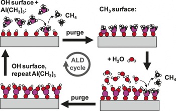
The critical defining feature of a “true ALD” process is that the half-reactions are self-limiting. Once the precursor has reacted with sites prepared during the previous co-reactant exposure, the surface reaction stops—that is, the surface sites prepared by the precursor reaction are reactive to the co-reactant, but not the precursor itself. This means that during steady-state growth, the precursor will typically deposit at most only one monolayer during each half-reaction cycle, even when the surface is exposed to the reactant species for long periods of time. One must ensure that enough precursor is delivered to achieve full saturation, otherwise, growth will be non-ideal and non-uniform.
A beneficial outcome of these self-saturated half-reactions is that long exposure times will permit the precursor and co-reactant to seek and find all available reaction sites on very non-planar or otherwise tortuous substrates, producing uniform and conformal growth without excess growth on the “top” of the sample.Reference Elam, Routkevitch, Markilovich and George9 The self-limiting nature of ALD half-reactions is achieved by matching the precursor and co-reactant and by controlling the deposition temperature. The precursor and reactant should react spontaneously on the surface, producing a desired surface-bound product and volatile vapor by-products. To achieve ALD growth, the temperature must be held low enough so that the precursor does not decompose during surface adsorption, but the temperature must be high enough to thermally activate the reaction and/or avoid surface condensation. This leads to a range of temperatures, commonly referred to as the “ALD window,” where the temperature is optimized to produce one monolayer of growth during each ALD cycle.
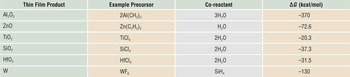
The growth rate within the ALD temperature “window” is determined by the density of available reactive sites on the surface and the optimum saturation occupancy of those sites by the adsorbed precursor, including steric effects of molecular packing density.Reference Puurunen3 For well-chosen reactants, this produces an ALD “thickness per cycle” growth rate that under controlled temperature is highly reproducible from lab-to-lab using different reactor designs and different saturated reactant exposure conditions. Table I presents several example precursor and reactant combinations used for ALD processing, including the overall ΔG of the reaction determined from calculated values.10 The overall ΔG for Al2O3 ALD is significantly more favorable than for other oxide materials.
Example precursors and co-reactants for some common atomic layer deposition materials and the free energy change for the overall deposition reaction.
We note that ALD is chemically distinct from CVD processes. During most CVD processes, the precursors (often the same ones used for ALD) are delivered concurrently to a heated growth surface. The surface temperature is often hotter than the temperature used in ALD, causing precursor dissociation at or near the growth surface, resulting in continuous growth. In CVD, the local growth rate is determined by steady-state precursor arrival flux and/or surface kinetics. In some variants of CVD, the reactants are delivered sequentially as in an ALD process. However, when the precursor dissociation is not self-limiting (as may occur if the temperature is too high or if the precursor dissociation pathway does not lead to a clear ALD temperature window), then the process may be better termed “pulsed CVD.” While these processes may show improved material properties or other beneficial aspects for some applications, they often display more non-uniform thickness and/or non-conformal growth.
History of ALD: Atomic layer epitaxy and molecular layering
The basic principle of self-limiting surface reactions is critical in understanding ALD.Reference Suntola and Antson1, Reference Suntola2, Reference George, Ott and Klaus11 The self-limiting nature of surface reactions produces the excellent conformality of ALD and the ability to coat high aspect ratio structures.Reference Elam, Routkevitch, Markilovich and George9 Self-limiting surface reactions also lead to film deposition that is not determined by statistics. The randomness of the precursor flux present in other chemical and physical vapor deposition processesReference Bray and Parsons12 is removed, and all reactions can be driven to completion during each surface reaction. This nonstatistical deposition yields extremely smooth deposited films with very little roughening as the deposition proceeds.Reference Fabreguette, Wind and George13
The term “ALD” began to be used commonly starting around 2000 when this deposition method emerged in semiconductor microelectronics, and ALD appeared as an important technique in the semiconductor roadmap. The key systems under development at this time were high-κ dielectrics for gate oxides in metal oxide semiconductor field-effect transistorsReference Mistry, Allen, Auth, Beattie, Bergstrom, Bost, Brazier, Buehler, Cappellani, Chau, Choi, Ding, Fischer, Ghani, Grover, Han, Hanken, Hatttendorf, He, Hicks, Huessner, Ingerly, Jain, James, Jong, Joshi, Kenyon, Kuhn, Lee, Liu, Maiz, McIntyre, Moon, Neirynck, Pei, Parker, Parsons, Prasad, Pipes, Prince, Ranade, Reynolds, Sandford, Schifren, Sebastian, Seiple, Simon, Sivakumar, Smith, Thomas, Troeger, Vandervoorn, Williams and Zawadzki6 and nanolaminate dielectric layers,Reference Kukli, Ihanus, Ritala and Leskelä14 for example, for low electron leakage dynamic random-access memory devices.Reference Kim, Lee, Choi, Park, Seo, Chin, Kim, Lim, Kim, Nam, Cho, Hwang, Kim, Kim, Park, Moon, Lee and Lee15, Reference Sneh, Clark-Phelps, Londergan, Winkler and Seidel16 Prior to this time, the term “atomic layer epitaxy” or ALE was in common use. Much of the ALE work in the 1990s focused on compound semiconductors, such as GaAs, that were crystalline. The transition from ALE to ALD resulted because many deposited films, such as the high-κ dielectrics, were amorphous and not epitaxial with the underlying substrate. Since the term “epitaxial” has come to imply a crystalline ordering with the underlying substrate, the more common amorphous films encountered in ALD, such as Al2O3 ALD, motivated the change in name.
The history of ALE dates back to the 1970s in Finland and the work of Suntola and associates. The first ALE process was ZnS, which was performed first using vaporized zinc and sulfur elements and later utilizing molecular diethyl zinc (DEZ) and hydrogen sulfide precursors.Reference Suntola2 Suntola’s work was motivated by device applications where improved growth processes could lead to controlled film thicknesses, pinhole-free insulators, and semiconducting films with better electrical properties.Reference Suntola and Antson1, Reference Suntola2 The first ALE patent was issued in 1977 to Suntola and Anston.Reference Suntola and Antson1 Suntola’s impact goes well beyond his development of the deposition processes. Many of the currently used ALD reactor designs were anticipated in Suntola’s patents, and most of the people within the strong ALD research and industry communities in Finland can readily trace their lineage back to Suntola.
The basic principles of self-limiting surface reactions were also under development in the former Soviet Union as early as the 1960s. This research, led by Aleskovskii at the Leningrad Lensovet Technological Institute (now Saint Petersburg State Institute of Technology), was known as “molecular layering,”Reference Aleskovskii17, Reference Malygin18 and was largely motivated by a need to better understand the basic building blocks of compound materials.Reference Aleskovskii17 Because most of this work was reported in Russian, much of the Western scientific community was not aware of this work until very recently. Even now, there are very few translations of the original Russian work and few citations of this work in any of the ALE or ALD literature. Recent work by Malygin at Saint Petersburg State Institute of Technology has publicized the original developments by Aleskovskii and co-workers.Reference Malygin18
Molecular layer deposition
MLD is one of the newer areas that will be highlighted in this introductory article. MLD is very similar to ALD and involves sequential, self-limiting surface reactions. However, a molecular fragment can be deposited during MLD. As mentioned in the article by Leskelä et al., the original work on MLD and the term “MLD” itself dates back to early work by Yoshimura in 1991 on pure organic polyimide polymers.Reference Yoshimura, Tatsuura and Sotoyama19 The growth of organic polymers by MLD uses surface chemistry that is modeled on condensation polymerization reactions.Reference George, Yoon and Dameron20 For example, self-limiting reaction schemes can be developed using bi-functional reactants such as diamines and dicarboxylic acids for polyamides.Reference Adamczyk, Dameron and George21 The MLD of organic polymers is somewhat limited by the low vapor pressure of organic precursors.
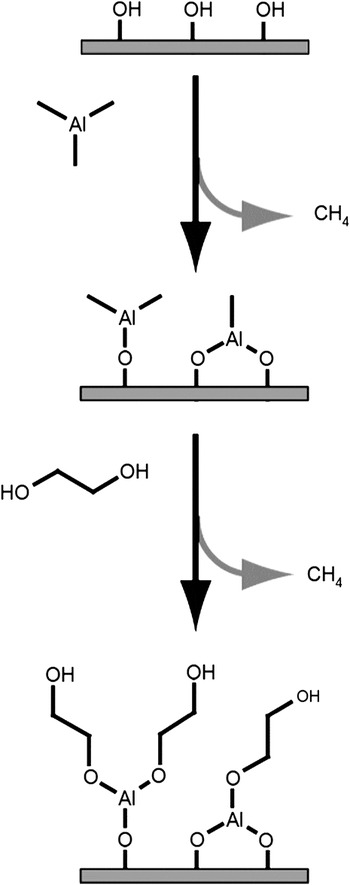
The MLD of hybrid organic-inorganic films offers many new possibilities for the growth of functional thin films. One of the first hybrid organic-inorganic films was an aluminum alkoxide polymer film grown using trimethylaluminum (TMA) and ethylene glycol (EG).Reference Dameron, Seghete, Burton, Davidson, Cavanagh, Bertrand and George22 This hybrid organic-inorganic is just one of a large family of aluminum alkoxides known as “alucones.”Reference McMahon, Alemany, Callender, Bott and Barron23 A schematic showing the surface chemistry of alucone growth using TMA and EG is shown in Figure 2.Reference Dameron, Seghete, Burton, Davidson, Cavanagh, Bertrand and George22 There are many parallels between the growth of alucone MLD using TMA and EG and Al2O3 ALD using TMA and H2O.
Schematic image of one cycle of molecular layer deposition leading to the formation of an “alucone” hybrid organic-inorganic thin film. Trimethylaluminum first reacts with hydroxyl groups to deposit -Al-CH3 surface species. Ethylene glycol then reacts with the Al-CH3 surface species to deposit –CH2CH2OH surface species. Reprinted with permission from Reference Reference Dameron, Seghete, Burton, Davidson, Cavanagh, Bertrand and George22. ©2008, American Chemical Society.
Many other hybrid organic-inorganic films can be fabricated using organometallic and organic precursors. For example, DEZ and various organic alcohols define zinc alkoxides that can be called “zincones.”Reference Yoon, O’Patchen, Seghete, Cavanagh and George24, Reference Peng, Gong, VanGundy and Parsons25 Likewise, titanium tetrachloride and organic alcohols define titanium alkoxides that can be called “titanicones.” The various metal alkoxides defined by reacting organometallics and organic alcohols can be known collectively as “metalcones.”Reference George, Lee, Yoon, Abdulagatov and Hall26 Additional classes of hybrid organic-inorganic films can be defined using other organic precursors such as carboxylic acids.Reference Klepper, Nilsen and Fjellvag27 The possibilities are nearly endless given the various organometallic precursors and large number of organic precursors. Combining ALD and MLD can also produce interesting organic-inorganic nanolaminate structures.Reference Salmi, Puukilainen, Vehkamaki, Heikkila and Ritala28
The key for future researchers will be to explore new uses for known hybrid organic-inorganic films and discover new hybrid materials that provide even more unique functionality. For example, the zincones may have electrical conductivity because of their similarity to ZnO.Reference Yoon, Lee, Derk, Musgrave and George29 The titanicones may display photocatalytic properties because of their similarity to TiO2. Because these hybrid organic-inorganic films contain organic constituents, they have some of the properties of organic polymers and may be applicable for flexible devices and flat panel displays.
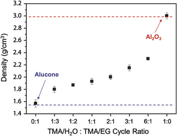
The many different types of hybrid organic-inorganic films grown by MLD can also be combined with their parent metal oxide grown by ALD to define alloys with composite properties. For example, alucone MLD and Al2O3 ALD can be combined by using various numbers of MLD and ALD reaction cycles to grow alucone alloy films. These alloys will have tunable properties that vary from pure MLD to pure ALD. Figure 3 shows the variable density of alucone alloys grown using various numbers of alucone MLD and Al2O3 ALD cycles. Other properties such as the elastic modulus, hardness, refractive index, and dielectric constant can be tuned over a wide range using metalcone alloys.
Thin film density plotted versus atomic layer deposition:molecular layer deposition (ALD:MLD) cycle ratio. Under MLD conditions (i.e., ALD:MLD cycle ratio = 0:1), the resulting alucone film has a density of ∼1.55 g/cm3. By introducing ALD cycles with the MLD cycles, the film density increases and reaches ∼3.0 g/cm3 for Al2O3 ALD (ALD:MLD = 1:0). The trend in density with a ALD:MLD ratio demonstrates the ability to form alumina/alucone alloys with a range of compositions. EG, ethylene glycol; TMA, trimethylaluminum. Reprinted with permission from Reference Reference George, Lee, Yoon, Abdulagatov and Hall26. ©2011, American Scientific Publishers.
Another exciting possibility is using the hybrid organic-inorganic films as a template for creating porous metal oxide films.Reference Peng, Gong, VanGundy and Parsons25, Reference Liang, Yu, Li, Jiang and Weimer30, Reference Qin, Yang, Scholz, Pippel, Lu and Knez31 The hybrid organic-inorganic MLD films can be deposited conformally on various substrates. After removing the organic constituent by thermal annealing, a conformal porous metal oxide film will be left on the substrate. The porosity may be tunable by varying the initial composition of the hybrid organic-inorganic MLD film or MLD-ALD alloy film. These conformal porous metal oxide films may have applications in catalysis and gas sensing where high surface area films offer many advantages.
Pulsed vapor infiltration and sequential vapor infiltration
While MLD is a strategy for bottom-up growth of polymer films and hybrid inorganic-organic coatings, the ALD process also enables a top-down approach to hybrid inorganic-organic or bio-inorganic materials preparation. Using time-separated delivery of precursors and reactants onto soft polymer surfaces in an ALD sequence, sub-surface diffusion and reaction can yield new coordinated or covalent organic-inorganic bonds within the polymer matrix. This sequential diffusion/reaction process can be referred to as multiple pulse infiltration, pulsed vapor infiltration, sequential vapor infiltration, or atomic layer deposition/infiltration.Reference Gong, Peng, Jur, Devine, Lee and Parsons32, Reference Lee, Pippel, Gosele, Dresbach, Qin, Chandran, Brauniger, Hause and Knez33
The interest in pulsed and sequential vapor infiltration methods lies in the composition, structure, and physical properties of the resulting hybrid organic-inorganic materials. Phenomenologically, Wilson et al.Reference Wilson, Grubbs and George34 observed that during ALD on polymers, precursors can infiltrate and react beneath the outer surface, forming a graded organic-inorganic interface. While sub-surface reactions are now known for several polymer/precursor combinations, more detailed studies of precursor interactions with soft substrates have revealed substantial dependence on the substrate and precursor. Some polymers with reactive surface groups do not show sub-surface diffusion, producing abrupt organic-inorganic interfaces during ALD.Reference Jur, Spagnola, Lee, Gong, Peng and Parsons35, Reference Zhang, Patil, Li, Schierhorn, Mann, Gosele and Knez36
Initial studies of vapor infiltration explored DEZ infusion and reaction with porphyrin dye fibers known as J-aggregates.Reference Jelley37, Reference Spagnola, Gong, Arvidson, Jur, Khan and Parsons38 The DEZ vapor reacts with the free base porphyrin to form a Zn-centered unit with a distinct optical response. Further studies with spider silks, collagen, and cellulose biopolymers, as well as polypropylene, polyamide-6, polytetrafluoroethylene (Teflon), and other organic polymers, showed interesting material and function modifications upon exposure to different metal-organic species and precursor/reactant combinations.Reference Gong, Peng, Jur, Devine, Lee and Parsons32, Reference Lee, Pippel, Gosele, Dresbach, Qin, Chandran, Brauniger, Hause and Knez33, Reference Jur, Spagnola, Lee, Gong, Peng and Parsons35, Reference Zhang, Patil, Li, Schierhorn, Mann, Gosele and Knez36, Reference Lee, Ischenko, Pippel, Masic, Moutanabbir, Fratzl and Knez39–Reference Peng, Tseng, Darling and Elam42
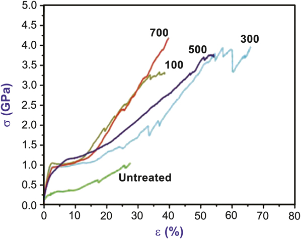
High surface-area polymer fibers are often a substrate of choice to observe and quantify reaction mechanisms and product outcomes during vapor infiltration. A good example of this is the study of TMA, titanium isopropoxide, and DEZ sequential vapor infiltration into native spider silk fibers.Reference Lee, Pippel, Gosele, Dresbach, Qin, Chandran, Brauniger, Hause and Knez33 In nature, biomaterials often complex metals (e.g., Zn, Cu) in order to gain strength or hardness.Reference Bryan and Gibbs43, Reference Gibbs and Bryan44 The idea behind the infiltration experiment was to artificially modify biomaterials to achieve metal complexes that are not common in nature. Figure 4 shows the resulting mechanical data when Araneus spider dragline silk is exposed at 70°C to 100, 300, 500, or 700 sequential cycles of TMA (30 seconds) and water (40 seconds). The overall toughness of the fiber (∫σ dε; σ is stress, and ε is strain) increased from ∼140 J/cm3 to nearly 1.4 kJ/cm3. Similar, but smaller, effects were also observed for vapor-infiltrated collagen.Reference Lee, Pippel, Moutanabbir, Gunkel, Thurn-Albrecht and Knez40
Stress (σ) versus strain (ε) mechanical response of dragline Araneus spider silk in the native untreated state and after exposure to the indicated number of trimethylaluminum (TMA)/water cycles at 70°C. During each cycle, the duration of the TMA and H2O exposure steps was 30 and 40 seconds, respectively, which is longer than ∼1 second exposures typically used for atomic layer deposition. The longer exposure time allowed reactants to diffuse into the natural polymer during each exposure step. The increased toughness (i.e., area under the stress–strain curve) upon TMA/water infiltration is ascribed to formation of metal–protein complexes aligned in strong protein chains. Adapted with permission from Reference Reference Lee, Pippel, Gosele, Dresbach, Qin, Chandran, Brauniger, Hause and Knez33. ©2009, AAAS.
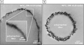
Delineating conditions that favor vapor infiltration versus ALD is often difficult. Species that diffuse rapidly in one polymer may diffuse slowly or not at all into another. Infrared spectroscopy results indicate, for example, that TMA readily diffuses into polypropylene, but TMA does not react with the polymer.Reference Zhang, Patil, Li, Schierhorn, Mann, Gosele and Knez36 At higher temperatures, enhanced diffusion leads to surface roughening that is not observed for coatings formed at lower temperatures (Figure 5).Reference Jur, Spagnola, Lee, Gong, Peng and Parsons35
Cross-sectional transmission electron micrographs of polypropylene exposed to 100 cycles of trimethylaluminum/water atomic layer deposition (ALD) at (a) 60°C and (b) 90°C. For deposition on polypropylene, the extent of penetration of the precursor and reactant into the bulk of the polymer depends significantly on deposition temperature. Reprinted with permission from Reference Reference Jur, Spagnola, Lee, Gong, Peng and Parsons35. ©2010, American Chemical Society.
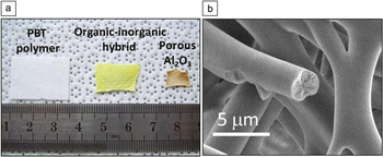
Pulsed or sequential vapor infiltration can also completely saturate the bulk/precursor reaction, yielding full chemical modification of the starting polymer. After exposing polybutylene terephthalate microfibers to TMA and H2O for 18 hours and 1 hour, respectively, at 80°C, mass uptake and infrared transmission data indicated that the starting polymer was completely converted to a hybrid organic-inorganic solid, as shown in Figure 6. Subsequent annealing in air at 450°C removed the organic component, leaving a highly porous inorganic structure that replicates the physical shape of the starting fiber.Reference Gong, Peng, Jur, Devine, Lee and Parsons32 Moreover, using different polyesters, the resulting pore size scales with the starting polymer repeat unit, showing capacity for chemical templating infiltration.
(a) Polybutylene terephthalate (PBT) nonwoven fiber mats as received, after trimethylaluminum/water sequential vapor infiltration, and after anneal at 450°C. The starting size for all samples was approximately the same. Sequential vapor infiltration penetrates throughout the 3 micron polymer fiber and transforms it into a hybrid organic-inorganic solid. Further annealing drives out the organic component yielding a mesoporous (5–10 nm pores) solid aluminum oxide with the same shape and form as the starting polymer. The porous oxide fiber is shown at the right side of part (a), and under magnification is shown in part (b). The pore size in the oxide correlates with the polymer repeat unit dimension, showing that the infiltration reaction successfully templates the starting polymer chemical structure. Adapted with permission from Reference Reference Gong, Peng, Jur, Devine, Lee and Parsons32. ©2011, American Chemical Society.
Synthesis via ALD-based infiltration yields unique material products not available through wet-chemical methods involving solvated metal ions, or continuous processes where reactants are delivered simultaneously.Reference Lee, Pippel and Knez45 Many vapor infiltration reaction schemes are possible and can produce a new class of “vapor-source” hybrids, with unique chemical structure, controlled physical response, and wide-ranging functional capability. These materials and processes have significant potential for continued exploration.
Summary
Beyond the history and technical introduction to atomic layer deposition (ALD), we present a brief glimpse into capabilities and possible outcomes for advanced ALD, molecular layer deposition (MLD), and sequential vapor infiltration processes to create new organic, inorganic, and hybrid organic-inorganic materials. To continue the advancement of this field, new research is especially needed in precursors, for example, to enable new ALD materials and achieve a better defined or a different “ALD window” for ALD processes that are currently known. New research on mechanical control, biological integration, and catalytic performance of ALD materials will also help expand application areas. Because of the complex interplay between precursors, reactants, and substrates, a plethora of novel materials with yet unknown properties remain to be synthesized. We still have a long way to go to fully understand and control key deposition and infiltration processes. Because the equipment needed for MLD and sequential vapor delivery builds directly on standard ALD, many researchers are now well poised to explore these and other reaction chemistries. Our hope is that the concepts and results presented in this issue will prompt new researchers to join this field and help broaden the scope and impact of ALD and ALD-based reaction technologies. While valuable progress has been made over the past 30+ years, we believe that the most significant advancements and impacts are still awaiting discovery and understanding.


