

1. Introduction
Wide band-gap III-V nitrides are very promising for application to high-power, high-frequency, and high-temperature electronic devices due to their superior properties, such as the large breakdown field and high electron velocity. For improvements in these devices, it is necessary to produce GaN and related compounds with low defect density. In the absence of a suitable GaN substrate, GaN is grown on highly lattice-mismatched substrates, such as Al2O3, GaAs and SiC. This leads to a high density of defects in the GaN that negatively impact optical and electrical properties. Therefore, a two-step growth consisting of pretreatment of the sapphire substrate prior to bulk growth was found to improve the quality of the GaN epitaxial layer Reference Amano, Sawaki, Akasaki and Toyoda[1]. Although these pretreatments do improve the crystal quality of the GaN, the nitridation effect on the crystal quality and lateral growth is not well understood.
In this letter, we demonstrate that the initial nitridation of the sapphire substrate plays a significant role in improving the crystal quality of GaN and proper nitridation enhances the grain size due to the promotion of the lateral growth. In particular, lower temperature nitridation, such as at 100 °C substrate temperature, can produce higher quality GaN and larger grain sizes.
2. Experimental Details
The samples were grown by molecular beam epitaxy (MBE) in a Riber 32 equipped with an EPI nitrogen source operated at 350W and 0.5 sccm, and a conventional Knudsen cell for Ga. Basal c-plane sapphire substrates were degreased using organic solvents (trichloroethylene, acetone and methanol) in an ultrasonic cleaner and rinsed with DI water. The tantalum-backed sapphire substrates were indium bonded on a silicon wafer and then mounted on an EPI uniblock using custom-made spring plates. After being loaded into the introduction chamber, the sapphire substrates were outgassed at 700°C for one hour. To investigate the effect of the nitridation on the GaN structural quality and grain size, a series of experiments on the nitridation of the sapphire substrates was performed using a range of temperatures from 100 to 700 °C. A 25nm thick GaN buffer was deposited at a temperature of 500°C. The temperature was raised to 800 °C to anneal the GaN buffer for 10min. A 0.9 μm thick GaN epitaxial layer was grown at 615 °C. Atomic force microscopy (AFM) measurements have been performed to determine the surface morphology of each of the layers after nitridation, buffer deposition, buffer annealing and bulk growth as a function of nitridation temperature. Only the nitridation and bulk results will be described here with more detailed results to follow in a subsequent publication. The crystal quality of the GaN films was measured by X-ray diffraction.
3. Discussions and Results
Nitridation of basal c-plane sapphire substrates was performed to investigate its effect on GaN structural quality and bulk grain size. The surface was exposed to N radicals as a function of temperature from 100 °C to 700 °C. Figure 1, Figure 2 and Figure 3 show AFM images of the surfaces of the sapphire substrate after exposure for one hour to the nitrogen plasma at 100 °C, 200 °C and 700°C, respectively. Substrate surface scratches that were introduced during the polishing process can be seen on the surfaces of all three samples. Figure 4 shows the surface roughness as a function of the nitridation substrate temperature. The root-mean-square surface roughness (R RMS) of 2μm×2μm scans increases with decreasing nitridation temperature. As also observed by Kim et al. Reference Kim, Yeadon, Botchkarev, Mohammad, Gibson and Morkoc[2], this data suggests that higher temperature nitridation retains the smooth surface of the sapphire substrate.
AFM image and RHEED pattern after one-hour nitridation at 100 °C [(a) and (b)].

AFM image and RHEED pattern after one-hour nitridation at 200 °C [(a) and (b)].

AFM image and RHEED pattern after one-hour nitridation at 700 °C [(a) and (b)].

Surface roughness after one-hour nitridation and GaN bulk growth as a function of temperature.

The RHEED patterns were observed to confirm the formation of a crystalline AlN or AlxN1−xO layer. The samples nitridated at lower substrate temperatures such as at 100 °C and 200°C show streaky patterns after one-hour nitridation, as shown in Figure 1 and 2. The RHEED pattern for sample nitridated at 100°C was blurry compared with those nitridated at higher temperature. It may result from transmission of the electron beam through the rougher sapphire surface at the 100 °C nitridation. Taferner et al. showed that the nitridation of the sapphire substrate at low substrate temperature, e.g. 200 °C, can also lead to the formation of AlN or AlxN1−xO layers Reference Taferner, Bensaoula, Kim and Bousetta[3]. AFM images after one-hour nitridation do not show any protrusions on the surfaces of the sapphire substrates, as shown in Figure 1, 2 and 3. These images suggest the formation of AlxN1−xO, instead of AlN layers. Heinlein et al. showed that the sapphire surface exposed to N plasma radicals started to form AlN around 300 min at 400 °C substrate temperature Reference Heinlein, Grepstad, Berge and Riechert[4], much longer than used in this study.
Thin GaN buffers (25nm) were deposited at 500 °C substrate temperature on the sapphire substrates nitridated at different substrate temperatures. This was followed by an anneal for 10min at 800 °C substrate temperature under nitrogen. The 0.9 μm GaN bulk was then grown under Ga stable growth conditions at 615 °C substrate temperature, at a growth rate of 0.9μm/hr.
The GaN crystal quality was characterized by the ω-scan of symmetric (0004) and asymmetric (10-5) reflecting planes with a Bede QC2a x-ray diffractometer. Figure 5 shows the X-ray rocking curve results as a function of the nitridation temperature. It is clearly shown that the GaN crystal quality improves with decreasing nitridation temperature. It is well known that the values of symmetric FWHM do not give information on the threading dislocations that include edge components. Thus, an asymmetric X-ray measurement is required for further quantification of the structural quality. The GaN films grown on sapphire substrates at low nitridation temperatures lead to lower symmetric and asymmetric full widths at half maximum of the x-ray rocking curves. The 0.9 μm GaN layers grown by MBE on the 100 °C nitridated sapphire substrate have x-ray rocking curve full width at half maximum (FWHM) of 136 arcsec (0004) and 261 arcsec (10-5). This compares to an x-ray rocking curve full width at half maximum of 818 arcsec (0004) for conventional MBE buffer conditions. For the conventional buffer, sapphire substrates were exposed to a N plasma at temperatures above 500 °C for 10min and then 25~50nm buffers were deposited without annealing at high temperature.
FWHM of the X-ray rocking curves for the symmetric and asymmetric reflections of 0.9μm-GaN bulk.

In order to investigate the effects of the nitridation on the GaN lateral growth as a function of the nitridation temperature, GaN films grown on nitridated substrates at different substrate temperatures were characterized by atomic force microscopy (AFM). The results are shown in Figure 6, Figure 7 and Figure 8. The 7.5μm×7.5μm AFM images show that there is the sudden change of the grain size from approximately 2μm to 2.4μm at 100 °C nitridation temperature. The largest grain size we can achieve was approximately 2.8μm at 100 °C nitridation temperature. However, the smoothest surface of the GaN was obtained at 200 °C nitridation temperature, as shown in Figure 4.
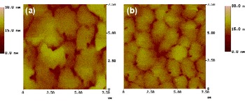
AFM images after the 0.9μm-GaN bulk growth at (a) 100°C, (b) 200°C for one-hour nitridation.
AFM images after the 0.9μm-GaN bulk growth at (a) 300°C, (b) 400°C for one-hour nitridation.

AFM image after the 0.9μm-GaN bulk growth at 700°C for one-hour nitridation.

4. Conclusion
The initial nitridation of the sapphire substrate strongly affects the crystal quality of the GaN. Low temperature nitridation can produce high quality and smooth GaN. GaN layers grown by plasma assisted MBE after 100 °C temperature nitridation for one-hour shows a full width at half maximum of the x-ray rocking curves of 136 and 261 arcsec for symmetric (0004) and asymmetric (10-5) reflections, respectively. However, conventional growth condition produces GaN films of 818 arcsec for symmetric (0004) full width at half maximum of x-ray rocking curves. An enhanced lateral growth was also observed in GaN layers on lower temperature nitridated sapphire substrate.
The authors would like to thank Dr. L. A. Bottomley for technical advice. This work was supported by the Office of Naval Research under Grant No. N00014-98-1-0209 monitored by Dr. Colin Wood.


